©
Semiconductor Components Industries, LLC, 2000
March, 2000 ≠ Rev. 3
1
Publication Order Number:
MC14521B/D
MC14521B
24-Stage Frequency Divider
The MC14521B consists of a chain of 24 flip≠flops with an input
circuit that allows three modes of operation. The input will function as
a crystal oscillator, an RC oscillator, or as an input buffer for an
external oscillator. Each flip≠flop divides the frequency of the
previous flip≠flop by two, consequently this part will count up to 2
24
=
16,777,216. The count advances on the negative going edge of the
clock. The outputs of the last seven≠stages are available for added
flexibility.
∑
All Stages are Resettable
∑
Reset Disables the RC Oscillator for Low Standby Power Drain
∑
RC and Crystal Oscillator Outputs Are Capable of Driving External
Loads
∑
Test Mode to Reduce Test Time
∑
V
DD
and V
SS
Pins Brought Out on Crystal Oscillator Inverter to
Allow the Connection of External Resistors for Low≠Power
Operation
∑
Supply Voltage Range = 3.0 Vdc to 18 Vdc
∑
Capable of Driving Two Low≠power TTL Loads or One Low≠power
Schottky TTL Load over the Rated Temperature Range.
MAXIMUM RATINGS
(Voltages Referenced to V
SS
) (Note 2.)
Symbol
Parameter
Value
Unit
V
DD
DC Supply Voltage Range
≠ 0.5 to +18.0
V
V
in
, V
out
Input or Output Voltage Range
(DC or Transient)
≠ 0.5 to V
DD
+ 0.5
V
I
in
, I
out
Input or Output Current
(DC or Transient) per Pin
±
10
mA
P
D
Power Dissipation,
per Package (Note 3.)
500
mW
T
A
Ambient Temperature Range
≠ 55 to +125
∞
C
T
stg
Storage Temperature Range
≠ 65 to +150
∞
C
T
L
Lead Temperature
(8≠Second Soldering)
260
∞
C
2. Maximum Ratings are those values beyond which damage to the device
may occur.
3. Temperature Derating:
Plastic "P and D/DW" Packages: ≠ 7.0 mW/
_
C From 65
_
C To 125
_
C
This device contains protection circuitry to guard against damage due to high
static voltages or electric fields. However, precautions must be taken to avoid
applications of any voltage higher than maximum rated voltages to this
high≠impedance circuit. For proper operation, V
in
and V
out
should be constrained
to the range V
SS
v
(V
in
or V
out
)
v
V
DD
.
Unused inputs must always be tied to an appropriate logic voltage level (e.g.,
either V
SS
or V
DD
). Unused outputs must be left open.
http://onsemi.com
A
= Assembly Location
WL or L
= Wafer Lot
YY or Y
= Year
WW or W = Work Week
Device
Package
Shipping
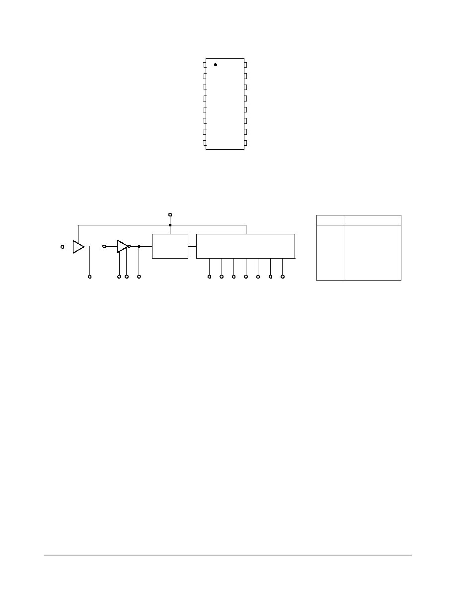
ORDERING INFORMATION
MC14521BCP
PDIP≠16
2000/Box
MC14521BD
SOIC≠16
48/Rail
MC14521BDR2
SOIC≠16
2500/Tape & Reel
1. For ordering information on the EIAJ version of
the SOIC packages, please contact your local
ON Semiconductor representative.
MARKING
DIAGRAMS
1
16
PDIP≠16
P SUFFIX
CASE 648
MC14521BCP
AWLYYWW
SOIC≠16
D SUFFIX
CASE 751B
1
16
14521B
AWLYWW
SOEIAJ≠16
F SUFFIX
CASE 966
1
16
MC14521B
AWLYWW
MC14521BFEL
SOEIAJ≠16
See Note 1.
MC14521BFR2
SOEIAJ≠16
See Note 1.
MC14521BF
SOEIAJ≠16
See Note 1.
MC14521B
http://onsemi.com
3
ŒŒŒŒŒŒŒŒŒŒŒŒŒŒŒŒŒŒŒŒŒŒŒŒŒŒŒŒŒŒŒŒŒ
ŒŒŒŒŒŒŒŒŒŒŒŒŒŒŒŒŒŒŒŒŒŒŒŒŒŒŒŒŒŒŒŒŒ
ELECTRICAL CHARACTERISTICS
(Voltages Referenced to V
SS
)
V
DD
≠ 55
_
C
25
_
C
125
_
C
Characteristic
Symbol
V
DD
Vdc
Min
Max
Min
Typ
(4.)
Max
Min
Max
Unit
Output Voltage
"0" Level
V
in
= V
DD
or 0
V
OL
5.0
10
15
--
--
--
0.05
0.05
0.05
--
--
--
0
0
0
0.05
0.05
0.05
--
--
--
0.05
0.05
0.05
Vdc
"1" Level
V
in
= 0 or V
DD
V
OH
5.0
10
15
4.95
9.95
14.95
--
--
--
4.95
9.95
14.95
5.0
10
15
--
--
--
4.95
9.95
14.95
--
--
--
Vdc
Input Voltage
"0" Level
(V
O
= 4.5 or 0.5 Vdc)
(V
O
= 9.0 or 1.0 Vdc)
(V
O
= 13.5 or 1.5 Vdc)
V
IL
5.0
10
15
--
--
--
1.5
3.0
4.0
--
--
--
2.25
4.50
6.75
1.5
3.0
4.0
--
--
--
1.5
3.0
4.0
Vdc
"1" Level
(V
O
= 0.5 or 4.5 Vdc)
(V
O
= 1.0 or 9.0 Vdc)
(V
O
= 1.5 or 13.5 Vdc)
V
IH
5.0
10
15
3.5
7.0
11
--
--
--
3.5
7.0
11
2.75
5.50
8.25
--
--
--
3.5
7.0
11
--
--
--
Vdc
Output Drive Current
(V
OH
= 2.5 Vdc)
Source
(V
OH
= 4.6 Vdc)
Pins 4 & 7
(V
OH
= 9.5 Vdc)
(V
OH
= 13.5 Vdc)
I
OH
5.0
5.0
10
15
≠ 1.2
≠ 0.25
≠ 0.62
≠ 1.8
--
--
--
--
≠ 1.0
≠ 0.2
≠ 0.5
≠ 1.5
≠ 1.7
≠ 0.36
≠ 0.9
≠ 3.5
--
--
--
--
≠ 0.7
≠ 0.14
≠ 0.35
≠ 1.1
--
--
--
--
mAdc
(V
OH
= 2.5 Vdc)
Source
(V
OH
= 4.6 Vdc)
Pins 1, 10,
(V
OH
= 9.5 Vdc)
11, 12, 13, 14
(V
OH
= 13.5 Vdc)
and 15
5.0
5.0
10
15
≠ 3.0
≠ 0.64
≠ 1.6
≠ 4.2
--
--
--
--
≠ 2.4
≠ 0.51
≠ 1.3
≠ 3.4
≠ 4.2
≠ 0.88
≠ 2.25
≠ 8.8
--
--
--
--
≠ 1.7
≠ 0.36
≠ 0.9
≠ 2.4
--
--
--
--
mAdc
(V
OL
= 0.4 Vdc)
Sink
(V
OL
= 0.5 Vdc)
(V
OL
= 1.5 Vdc)
I
OL
5.0
10
15
0.64
1.6
4.2
--
--
--
0.51
1.3
3.4
0.88
2.25
8.8
--
--
--
0.36
0.9
2.4
--
--
--
mAdc
Input Current
I
in
15
--
±
0.1
--
±
0.00001
±
0.1
--
±
1.0
µ
Adc
Input Capacitance
(V
in
= 0)
C
in
--
--
--
--
5.0
7.5
--
--
pF
Quiescent Current
(Per Package)
I
DD
5.0
10
15
--
--
--
5.0
10
20
--
--
--
0.005
0.010
0.015
5.0
10
20
--
--
--
150
300
600
µ
Adc
Total Supply Current
(5.) (6.)
(Dynamic plus Quiescent,
Per Package)
(C
L
= 50 pF on all outputs, all
buffers switching)
I
T
5.0
10
15
I
T
= (0.42
µ
A/kHz) f + I
DD
I
T
= (0.85
µ
A/kHz) f + I
DD
I
T
= (1.40
µ
A/kHz) f + I
DD
µ
Adc
4. Data labelled "Typ" is not to be used for design purposes but is intended as an indication of the IC's potential performance.
5. The formulas given are for the typical characteristics only at 25
_
C.
6. To calculate total supply current at loads other than 50 pF:
I
T
(C
L
) = I
T
(50 pF) + (C
L
≠ 50) Vfk
where: I
T
is in
µ
A (per package), C
L
in pF, V = (V
DD
≠ V
SS
) in volts, f in kHz is input frequency, and k = 0.003.

MC14521B
http://onsemi.com
4
ŒŒŒŒŒŒŒŒŒŒŒŒŒŒŒŒŒŒŒŒŒŒŒŒŒŒŒŒŒŒŒŒŒ
ŒŒŒŒŒŒŒŒŒŒŒŒŒŒŒŒŒŒŒŒŒŒŒŒŒŒŒŒŒŒŒŒŒ
SWITCHING CHARACTERISTICS
(7.)
(C
L
= 50 pF, T
A
= 25
_
C)
Characteristic
Symbol
V
DD
Vdc
Min
Typ
(8.)
Max
Unit
Output Rise and Fall Time (Counter Outputs)
t
TLH
, t
THL
= (1.5 ns/pF) C
L
+ 25 ns
t
TLH
, t
THL
= (0.75 ns/pF) C
L
+ 12.5 ns
t
TLH
, t
THL
= (0.55 ns/pF) C
L
+ 12.5 ns
t
TLH
, t
THL
5.0
10
15
--
--
--
100
50
40
200
100
80
ns
Propagation Delay Time
Clock to Q18
t
PHL
, t
PLH
= (1.7 ns/pF) C
L
+ 4415 ns
t
PHL
, t
PLH
= (0.66 ns/pF) C
L
+ 1667 ns
t
PHL
, t
PLH
= (0.5 ns/pF) C
L
+ 1275 ns
t
PHL
, t
PLH
5.0
10
15
--
--
--
4.5
1.7
1.3
9.0
3.5
2.7
µ
s
Clock to Q24
t
PHL
, t
PLH
= (1.7 ns/pF) C
L
+ 5915 ns
t
PHL
, t
PLH
= (0.66 ns/pF) C
L
+ 2167 ns
t
PHL
, t
PLH
= (0.5 ns/pF) C
L
+ 1675 ns
5.0
10
15
--
--
--
6.0
2.2
1.7
12
4.5
3.5
Propagation Delay Time
Reset to Q
n
t
PHL
= (1.7 ns/pF) C
L
+ 1215 ns
t
PHL
= (0.66 ns/pF) C
L
+ 467 ns
t
PHL
= (0.5 ns/pF) C
L
+ 350 ns
t
PHL
5.0
10
15
--
--
--
1300
500
375
2600
1000
750
ns
Clock Pulse Width
t
WH(cl)
5.0
10
15
385
150
120
140
55
40
--
--
--
ns
Clock Pulse Frequency
f
cl
5.0
10
15
--
--
--
3.5
9.0
12
2.0
5.0
6.5
MHz
Clock Rise and Fall Time
t
TLH
, t
THL
5.0
10
15
--
--
--
--
--
--
15
5.0
4.0
µ
s
Reset Pulse Width
t
WH(R)
5.0
10
15
1400
600
450
700
300
225
--
--
--
ns
Reset Removal Time
t
rem
5.0
10
15
30
0
≠ 40
≠ 200
≠ 160
≠ 110
--
--
--
ns
7. The formulas given are for the typical characteristics only at 25
_
C.
8. Data labelled "Typ" is not to be used for design purposes but is intended as an indication of the IC's potential performance.
Figure 1. Power Dissipation Test Circuit and Waveform
PULSE
GENERATOR
V
DD
V
DD
V
DD
V
SS
V
SS
Q18
Q19
Q20
Q21
Q22
Q23
Q24
C
L
C
L
C
L
C
L
C
L
C
L
C
L
I
D
IN 2
R
500
µ
F
0.01
µ
F
CERAMIC
20 ns
20 ns
V
DD
0 V
V
in
50% DUTY CYCLE
90%
10%
50%

MC14521B
http://onsemi.com
5
Figure 2. Switching Time Test Circuit and Waveforms
PULSE
GENERATOR
Q18
Q19
Q20
Q21
Q22
Q23
Q24
IN 2
R
V
DD
V
DD
V
SS
V
SS
C
L
C
L
C
L
C
L
C
L
C
L
C
L
V
DD
20 ns
20 ns
20 ns
10%
50%
90%
10%
50%
90%
IN 2
Q
n
t
PLH
t
PHL
t
TLH
t
THL
t
WL
t
WH
Characteristic
500 kHz
Circuit
50 kHz
Circuit
Unit
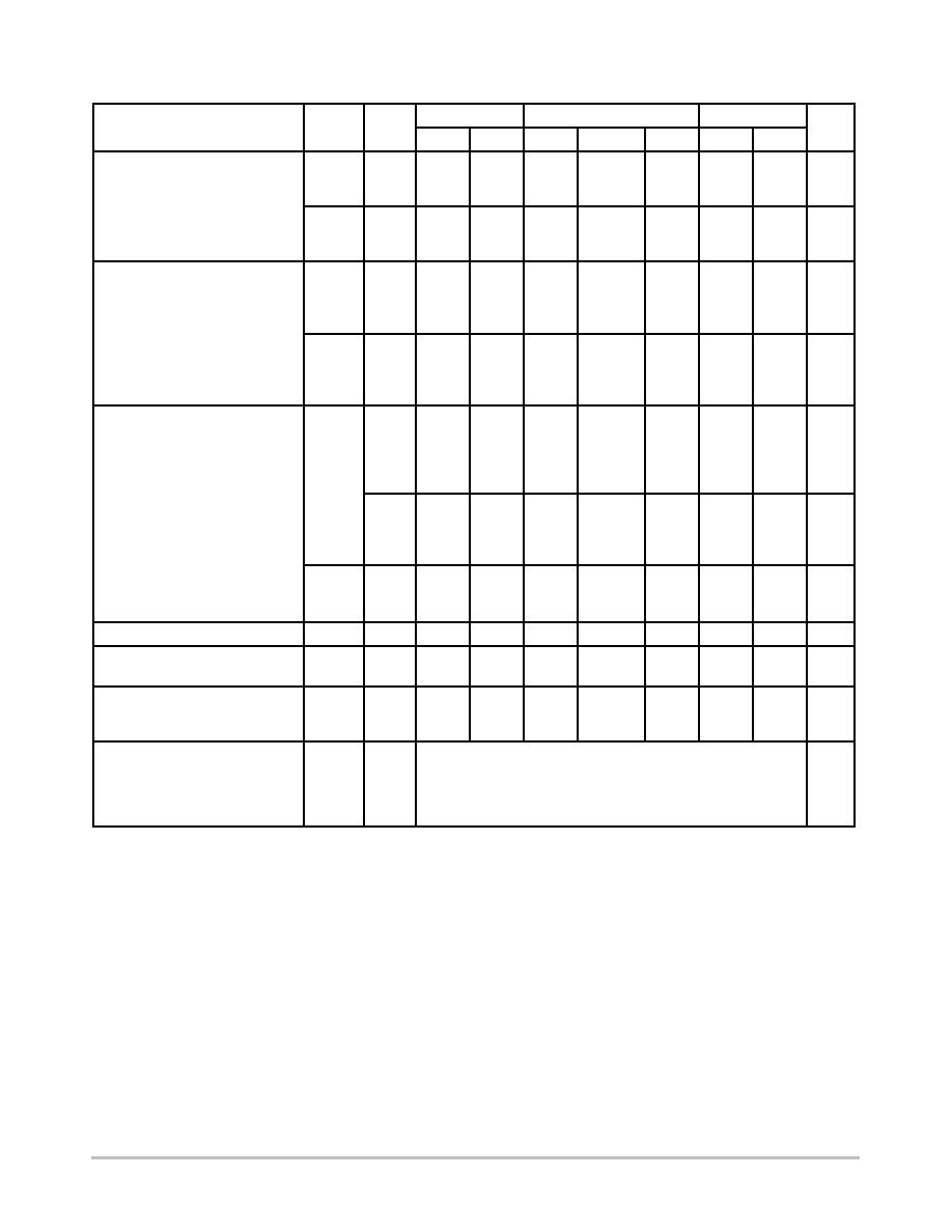
Crystal Characteristics
Resonant Frequency
Equivalent Resistance, R
S
500
1.0
50
6.2
kHz
k
External Resistor/Capacitor Values
R
o
C
T
C
S
47
82
20
750
82
20
k
pF
pF
Frequency Stability
Frequency Change as a Function
of V
DD
(T
A
= 25
_
C)
V
DD
Change from 5.0 V to 10 V
V
DD
Change from 10 V to 15 V
Frequency Change as a Function
of Temperature (V
DD
= 10 V)
T
A
Change from ≠ 55
_
C to + 25
_
C
MC14521 only
Complete Oscillator*
T
A
Change from + 25
_
C to + 125
_
C
MC14521 only
Complete Oscillator*
+ 6.0
+ 2.0
≠ 4.0
+ 100
≠ 2.0
≠ 160
+ 2.0
+ 2.0
≠ 2.0
+ 120
≠ 2.0
≠ 560
ppm
ppm
ppm
ppm
ppm
ppm
*Complete oscillator includes crystal, capacitors, and resistors.
ŒŒŒŒŒŒŒŒŒŒŒŒŒŒŒŒŒŒŒ
Œ
ŒŒŒŒŒŒŒŒŒŒŒŒŒŒŒŒŒ
Œ
ŒŒŒŒŒŒŒŒŒŒŒŒŒŒŒŒŒŒŒ
Figure 4. Typical Data for Crystal Oscillator Circuit
Figure 3. Crystal Oscillator Circuit
V
DD
V
DD
V
DD
V
SS
V
SS
OUT 1
OUT 2
Q18
Q19
Q20
Q21
Q22
Q23
Q24
IN 1
IN 2
R
R*
R*
C
S
C
T
R
o
18 M
* Optional for low power operation,
10 k
R
70 k
.