 | –≠–ª–µ–∫—Ç—Ä–æ–Ω–Ω—ã–π –∫–æ–º–ø–æ–Ω–µ–Ω—Ç: NB4L339 | –°–∫–∞—á–∞—Ç—å:  PDF PDF  ZIP ZIP |

© Semiconductor Components Industries, LLC, 2006
September, 2006 - Rev. 0
1
Publication Order Number:
NB3N2304NZ/D
NB3N2304NZ
3.3V 1:4 Clock Fanout
Buffer
Description
The NB3N2304NZ is a low skew 1-to 4 clock fanout buffer,
designed for high speed clock distribution such as in PCI-X
applications. The NB3N2304NZ guarantees low output-to-output
skew. Optimal design, layout and processing minimizes skew within a
device and from device-to-device.
The Output Enable (OE) pin forces the outputs LOW when LOW.
Features
∑
Input/Output Clock Frequency up to 140 MHz
∑
Low Skew Outputs (100 ps)
∑
Output Enable
∑
Operating Range: V
DD
= 3.0 V to 3.6 V
∑
Ideal for PCI-X and networking clocks
∑
Packaged in 8-pin TSSOP, 4.4 mm x 3 mm
∑
Industrial Temperature Range
∑
These are Pb-Free Devices*
*For additional information on our Pb-Free strategy and soldering details, please
download the ON Semiconductor Soldering and Mounting Techniques
Reference Manual, SOLDERRM/D.
TSSOP-8
DT SUFFIX
CASE 948S
MARKING
DIAGRAM*
http://onsemi.com
*For additional marking information, refer to
Application Note AND8002/D.
See detailed ordering and shipping information in the package
dimensions section on page 5 of this data sheet.
ORDERING INFORMATION
Figure 1. Simplified Logic Diagram
NB3N
2304
YWWA G
A
= Assembly Location
Y
= Year
WW = Work Week
G
= Pb-Free Package
DFN8
TBD SUFFIX
CASE 506AA
XX M
1
4
1

NB3N2304NZ
http://onsemi.com
2
Figure 2. Block Diagram
Figure 3. NB3N2304NZ Package Pinout (Top View)
Q1
Q2
Q3
Q4
IN
Logic
Control
OE
1
2
3
4
8
7
6
5
Q4
Q3
V
DD
Q2
IN
OE
Q1
GND
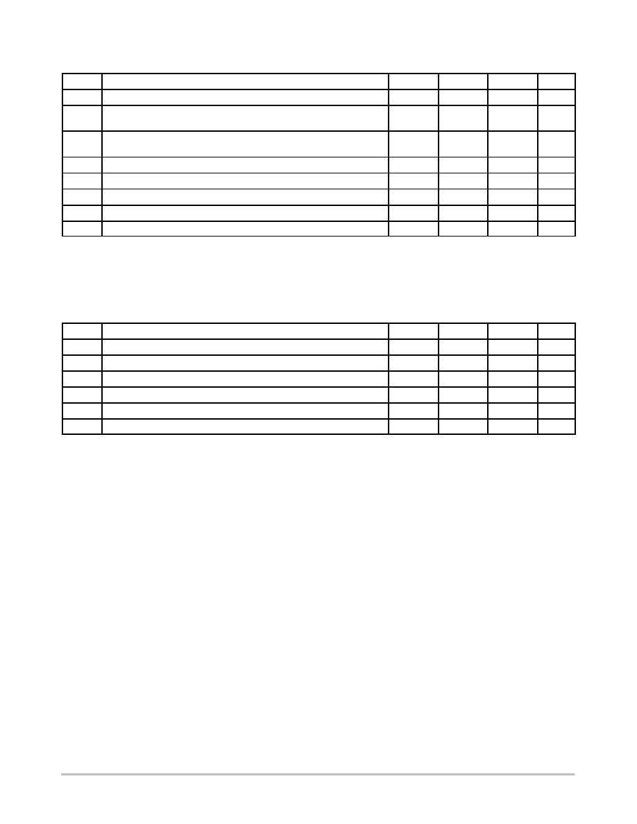
Table 1. PIN DESCRIPTION
Pin #
Pin
Name
Type
Description
1
IN
LVCMOS/LVTTL Input
Clock Input
2
OE
LVCMOS/LVTTL Input
Output Enable for the clock outputs. Outputs are enabled when forced HIGH. Outputs
are forced to logic LOW when OE is forced LOW.
3
Q1
LVCMOS/LVTTL Output
Clock Output 1
4
GND
Power
Negative Supply Voltage; Connect to Ground, 0 V
5
Q2
(LV)CMOS/(LV)TTL Input
Clock Output 2
6
V
DD
Power
Positive Supply Voltage (3.0 V to 3.6 V)
7
Q3
(LV)CMOS/(LV)TTL Output
Clock Output 3
8
Q4
(LV)CMOS/(LV)TTL Input
Clock Output 4
Table 2. OE, OUTPUT ENABLE FUNCTION TABLE
Inputs
Outputs
IN
OE
L
L
L
H
L
L
L
H
L
H
H
H

NB3N2304NZ
http://onsemi.com
3
Table 3. ATTRIBUTES
Characteristics
Value
ESD Protection
Human Body Model
Machine Model
> 2kV
> 200 V
Moisture Sensitivity, Indefinite Time Out of Drypack (Note 1)
Level 1
Flammability Rating
Oxygen Index: 28 to 34
UL 94 V-O @ 0.125 in
Transistor Count
480 Devices
Meets or exceeds JEDEC Spec EIA/JESD78 IC Latchup Test
1. For additional information, see Application Note AND8003/D.
Table 4. MAXIMUM RATINGS
Symbol
Parameter
Condition 1
Condition 2
Rating
Unit
V
DD
Positive Power Supply
GND = 0 V
V
DD
+ 0.5V
V
V
I
Input Voltage
GND ≠ 0.5 v
V
I
v V
DD
+ 0.5
V
T
A
Operating Temperature Range, Industrial
w -40 to v +85
∞C
T
stg
Storage Temperature Range
-65 to +150
∞C
q
JA
Thermal Resistance (Junction-to-Ambient)
0 lfpm
500 lfpm
TSSOP-8
∞C/W
∞C/W
q
JC
Thermal Resistance (Junction-to-Case)
TSSOP-8
∞C/W
T
SOL
Wave Solder
Pb-Free (Note 2)
265
∞C
Stresses exceeding Maximum Ratings may damage the device. Maximum Ratings are stress ratings only. Functional operation above the
Recommended Operating Conditions is not implied. Extended exposure to stresses above the Recommended Operating Conditions may affect
device reliability.
2. EDEC standard multilayer board - 2S2P (2 signal, 2 power).
NB3N2304NZ
http://onsemi.com
4
Table 5. DC CHARACTERISTICS
V
DD
= 3.0 V to 3.6 V, GND = 0 V, T
A
= -40∞C to +85∞C
Symbol
Characteristic
Min
Typ
Max
Unit
I
DD
Power Supply Current @ 66.66 MHz, Unloaded Outputs
12
25
mA
V
OH
Output HIGH Voltage
- IOH = -24 mA
-IOH = -12 mA
2.0
2.4
V
V
OL
Output LOW Voltage
-IOL = 24 mA
-IOL = 12 mA
0.8
0.55
V
V
IH
Input HIGH Voltage, IN and OE (Note 3)
2.0
V
V
IL
Input LOW Voltage, IN and OE (Note 3)
0.8
V
I
IH
Input HIGH Current, V
IN
= V
DD
-50
50
mA
I
IL
Input LOW Current, V
IN
= 0 V
-100
100
mA
CIN
Input Capacitance, IN, OE
5
7
pF
NOTE: Device will meet the specifications after thermal equilibrium has been established when mounted in a test socket or printed circuit
board with maintained transverse airflow greater than 500 lfpm. Electrical parameters are guaranteed only over the declared
operating temperature range. Functional operation of the device exceeding these conditions is not implied. Device specification limit
values are applied individually under normal operating conditions and not valid simultaneously.
3. IN input has a threshold voltage of V
DD
/2.
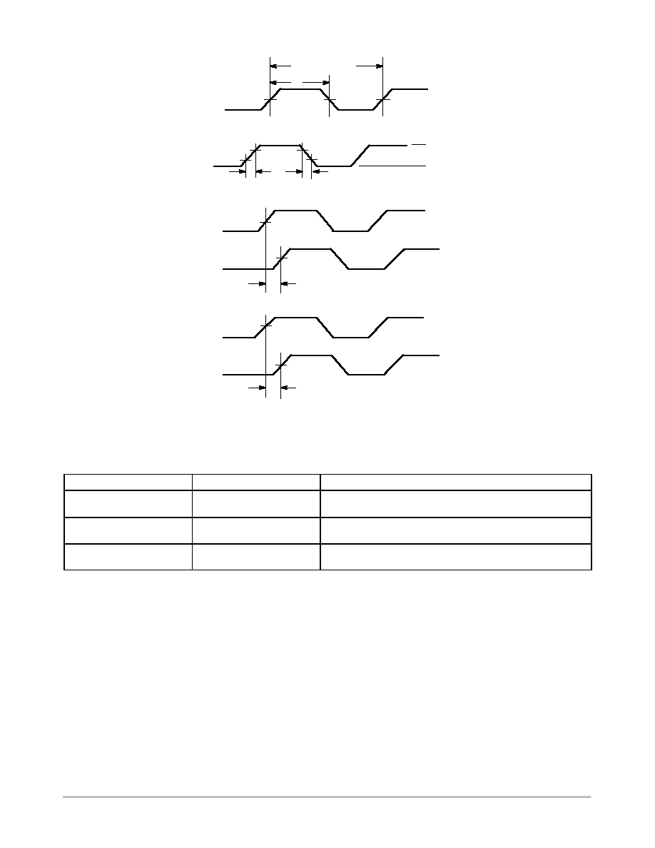
Table 6. AC CHARACTERISTICS
V
DD
= 3.0 V to 3.6 V, GND = 0 V, T
A
= -40∞C to +85∞C (Note 4) (Figure 4)
Symbol
Characteristic
Min
Typ
Max
Unit
f
in
Input Clock Frequency
DC
140
MHz
t
DCskew
Duty Cycle Skew = t2 ˜ t1 (Figure 4) Measured at 1.5 V
40
50
60
%
tr/tf
Output Rise and Fall Times; 0.8 V to 2.0 V
0.9
1.5
ns
t
pd
Propagation Delay, IN-to-Qn (Note 5)
2.5
3.5
5
ns
t
skew
Output-to-Output Skew; (Note 5)
100
ps
t
pu
Powerup Time for V
DD
to Reach Minimum Specified Voltage
0.05
50
ms
NOTE: Device will meet the specifications after thermal equilibrium has been established when mounted in a test socket or printed circuit
board with maintained transverse airflow greater than 500 lfpm. Electrical parameters are guaranteed only over the declared
operating temperature range. Functional operation of the device exceeding these conditions is not implied. Device specification limit
values are applied individually under normal operating conditions and not valid simultaneously.
4. All outputs loaded equally with C
L
= 25 pF to GND. Duty cycle out = duty in. A 0.01 mF decoupling capacitor should be connected between
V
DD
and GND.
5. Measured on rising edges at V
DD
B 2; all outputs with equal loading.
NB3N2304NZ
http://onsemi.com
5
Figure 4. Switching Waveforms
Duty Cycle Timing
All Outputs Rise/Fall Time
Output-Output Skew
Input-Output Propagation Delay
1.5 V
1.5 V
2.0 V
0.8 V
0.8 V
2.0 V
1.5 V
1.5 V
1.5 V
3.3 V
0 V
OUTPUT
OUTPUT
INPUT
OUTPUT
OUTPUT
t
1
t
2
t
r
t
f
t
SKEW
V
DD
/2
V
DD
/2
t
pd
ORDERING INFORMATION
Device
Package
Shipping
NB3N2304NZDTG
TSSOP-8
(Pb-Free)
100 Units / Rail
NB3N2304NZDTR2G
TSSOP-8
(Pb-Free)
2500 / Tape & Reel
NB3N2304NZMNR4G*
DFN8
(Pb-Free)
1000 / Tape & Reel
For information on tape and reel specifications, including part orientation and tape sizes, please refer to our Tape and Reel Packaging
Specifications Brochure, BRD8011/D.
*Contact a sales representative.

NB3N2304NZ
http://onsemi.com
6
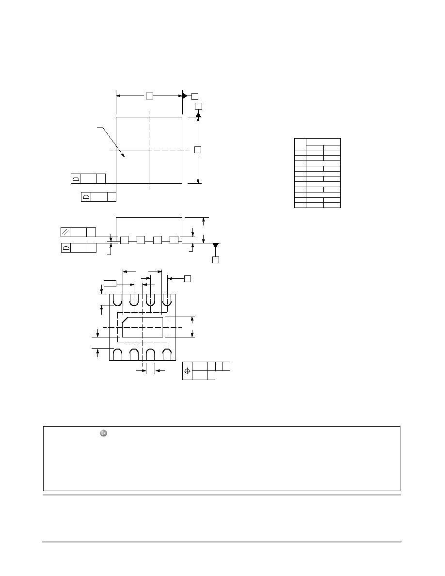
PACKAGE DIMENSIONS
TSSOP-8
CASE 948S-01
ISSUE B
DIM
MIN
MAX
MIN
MAX
INCHES
MILLIMETERS
A
2.90
3.10
0.114
0.122
B
4.30
4.50
0.169
0.177
C
---
1.10
---
0.043
D
0.05
0.15
0.002
0.006
F
0.50
0.70
0.020
0.028
G
0.65 BSC
0.026 BSC
L
6.40 BSC
0.252 BSC
M
0
8
0
8
NOTES:
1. DIMENSIONING AND TOLERANCING PER ANSI
Y14.5M, 1982.
2. CONTROLLING DIMENSION: MILLIMETER.
3. DIMENSION A DOES NOT INCLUDE MOLD FLASH.
PROTRUSIONS OR GATE BURRS. MOLD FLASH
OR GATE BURRS SHALL NOT EXCEED 0.15
(0.006) PER SIDE.
4. DIMENSION B DOES NOT INCLUDE INTERLEAD
FLASH OR PROTRUSION. INTERLEAD FLASH OR
PROTRUSION SHALL NOT EXCEED 0.25 (0.010)
PER SIDE.
5. TERMINAL NUMBERS ARE SHOWN FOR
REFERENCE ONLY.
6. DIMENSION A AND B ARE TO BE DETERMINED
AT DATUM PLANE -W-.
_
_
_
_
SEATING
PLANE
PIN 1
1
4
8
5
DETAIL E
B
C
D
A
G
L
2X
L/2
-U-
S
U
0.20 (0.008) T
S
U
M
0.10 (0.004)
V
S
T
0.076 (0.003)
-T-
-V-
-W-
8x REF
K
IDENT
K
0.19
0.30
0.007
0.012
S
U
0.20 (0.008) T
P1
P
DETAIL E
F
M
0.25 (0.010)
…………
…………
…………
«««
«««
K1
K
J J1
SECTION N-N
J
0.09
0.20
0.004
0.008
K1
0.19
0.25
0.007
0.010
J1
0.09
0.16
0.004
0.006
P
---
2.20
---
0.087
P1
---
3.20
---
0.126
N
N
NB3N2304NZ
http://onsemi.com
7
PACKAGE DIMENSIONS
DFN8
CASE 506AA-01
ISSUE D
NOTES:
1. DIMENSIONING AND TOLERANCING PER
ASME Y14.5M, 1994 .
2. CONTROLLING DIMENSION: MILLIMETERS.
3. DIMENSION b APPLIES TO PLATED
TERMINAL AND IS MEASURED BETWEEN
0.25 AND 0.30 MM FROM TERMINAL.
4. COPLANARITY APPLIES TO THE EXPOSED
PAD AS WELL AS THE TERMINALS.
««««
««««
««««
««««
A
D
E
B
C
0.10
PIN ONE
2 X
REFERENCE
2 X
TOP VIEW
SIDE VIEW
BOTTOM VIEW
A
L
(A3)
D2
E2
C
C
0.10
C
0.10
C
0.08
8 X
A1
SEATING
PLANE
e/2
e
8 X
K
NOTE 3
b
8 X
0.10 C
0.05 C
A BB
DIM
MIN
MAX
MILLIMETERS
A
0.80
1.00
A1
0.00
0.05
A3
0.20 REF
b
0.20
0.30
D
2.00 BSC
D2
1.10
1.30
E
2.00 BSC
E2
0.70
0.90
e
0.50 BSC
K
0.20
---
L
0.25
0.35
1
4
8
5
ON Semiconductor and are registered trademarks of Semiconductor Components Industries, LLC (SCILLC). SCILLC reserves the right to make changes without further notice
to any products herein. SCILLC makes no warranty, representation or guarantee regarding the suitability of its products for any particular purpose, nor does SCILLC assume any liability
arising out of the application or use of any product or circuit, and specifically disclaims any and all liability, including without limitation special, consequential or incidental damages.
"Typical" parameters which may be provided in SCILLC data sheets and/or specifications can and do vary in different applications and actual performance may vary over time. All
operating parameters, including "Typicals" must be validated for each customer application by customer's technical experts. SCILLC does not convey any license under its patent rights
nor the rights of others. SCILLC products are not designed, intended, or authorized for use as components in systems intended for surgical implant into the body, or other applications
intended to support or sustain life, or for any other application in which the failure of the SCILLC product could create a situation where personal injury or death may occur. Should
Buyer purchase or use SCILLC products for any such unintended or unauthorized application, Buyer shall indemnify and hold SCILLC and its officers, employees, subsidiaries, affiliates,
and distributors harmless against all claims, costs, damages, and expenses, and reasonable attorney fees arising out of, directly or indirectly, any claim of personal injury or death
associated with such unintended or unauthorized use, even if such claim alleges that SCILLC was negligent regarding the design or manufacture of the part. SCILLC is an Equal
Opportunity/Affirmative Action Employer. This literature is subject to all applicable copyright laws and is not for resale in any manner.
PUBLICATION ORDERING INFORMATION
N. American Technical Support: 800-282-9855 Toll Free
USA/Canada
Europe, Middle East and Africa Technical Support:
Phone: 421 33 790 2910
Japan Customer Focus Center
Phone: 81-3-5773-3850
NB3N2304NZ/D
LITERATURE FULFILLMENT:
Literature Distribution Center for ON Semiconductor
P.O. Box 5163, Denver, Colorado 80217 USA
Phone: 303-675-2175 or 800-344-3860 Toll Free USA/Canada
Fax: 303-675-2176 or 800-344-3867 Toll Free USA/Canada
Email: orderlit@onsemi.com
ON Semiconductor Website: www.onsemi.com
Order Literature: http://www.onsemi.com/orderlit
For additional information, please contact your local
Sales Representative