Äîêóìåíòàöèÿ è îïèñàíèÿ www.docs.chipfind.ru
© Semiconductor Components Industries, LLC, 2006
August, 2006 - Rev. 1
1
Publication Order Number:
NB4L6254/D
NB4L6254
2.5V / 3.3V Differential
LVPECL 2x2 Clock Switch
and Low Skew Fanout
Buffer
Description
The NB4L6254 is a differential 2x2 clock switch and drives
precisely aligned clock signals through its LVPECL fanout buffers. It
employs a fully differential architecture with bipolar technology,
offers superior digital signal characteristics, has very low clock output
skew and supports clock frequencies from DC up to 3.0 GHz.
The NB4L6254 is designed for the most demanding, skew critical
differential clock distribution systems. Typical applications for the
NB4L6254 are clock distribution, switching and data loopback
systems of high-performance computer, networking and
telecommunication systems, as well as on-board clocking of OC-3,
OC-12 and OC-48 communication systems. In addition, the
NB4L6254 can be configured as a single 1:6 or dual 1:3 LVPECL
fanout buffer.
The NB4L6254 can be operated from a single 3.3 V or 2.5 V power
supply.
Features
·
Maximum Clock Input Frequency, 3 GHz
·
Maximum Input Data Rate, 3 Gb/s
·
Differential LVPECL Inputs and Outputs
·
Low Output Skew: 50 ps Maximum Output-to-Output Skew
·
Synchronous Output Enable Eliminating Output Runt Pulse
Generation and Metastability
·
Operating Range: Single 3.3 V or 2.5 V Supply
V
CC
= 2.375 V to 3.465 V
·
LVCMOS Compatible Control Inputs
·
Packaged in LQFP-32
·
Fully Differential Architecture
·
-40°C to 85°C Ambient Operating Temperature
·
These are Pb-Free Devices*
*For additional information on our Pb-Free strategy and soldering details, please
download the ON Semiconductor Soldering and Mounting Techniques
Reference Manual, SOLDERRM/D.
LQFP-32
FA SUFFIX
CASE 873A
MARKING
DIAGRAM*
http://onsemi.com
*For additional marking information, refer to
Application Note AND8002/D.
See detailed ordering and shipping information in the package
dimensions section on page 7 of this data sheet.
ORDERING INFORMATION
A
= Assembly Location
WL
= Wafer Lot
YY
= Year
WW
= Work Week
G
= Pb-Free Package
NB4L
6254
AWLYYWWG
OEA
QA0
QA0
QA1
QA1
QA2
QA2
QB0
QB0
QB1
QB1
QB2
QB2
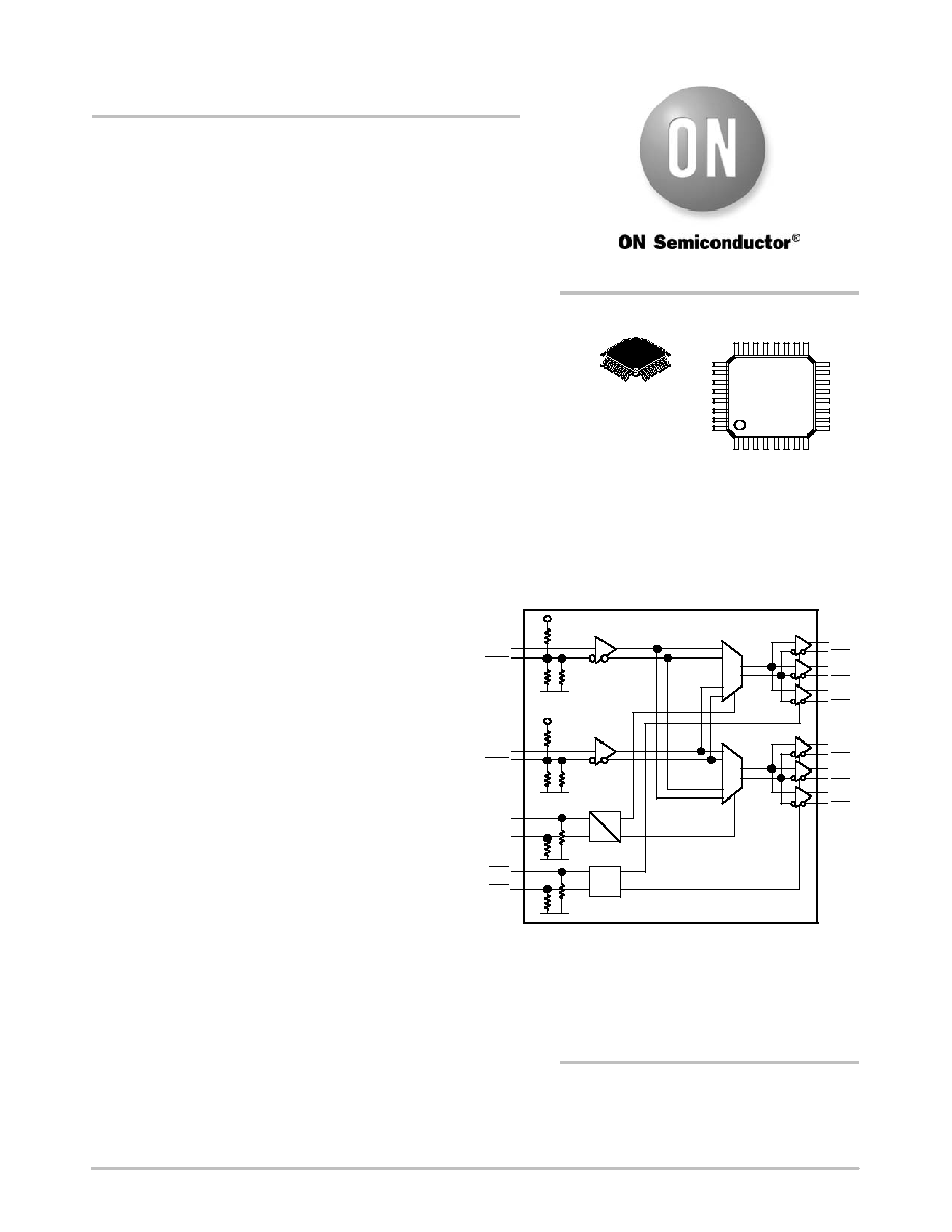
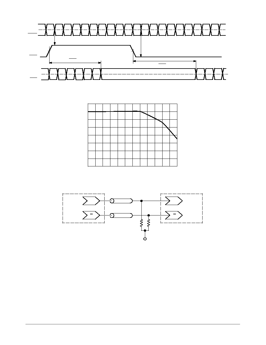
0
1
0
1
Bank A
Bank B
OEB
SEL0
SEL1
CLK1
CLK1
CLK0
CLK0
V
CC
V
CC
Figure 1. Functional Block Diagram
NB4L6254
http://onsemi.com
2
25
26
27
28
29
30
31
32
15
14
13
12
11
10
9
1
2
3
4
5
6
7
8
24
23
22
21
20
19
18
17
16
GND
V
CC
OEA CLK0 CLK0
V
CC
SEL0 GND
QB2
QB2
QB1
QB1
QB0
QB0
QA2
QA2
V
CC
V
CC
OEB
CLK1
QA1
V
CC
GND
V
CC
QA1
V
CC
QA0
QA0
GND SEL1
CLK1
V
CC
Figure 2. Pin Configuration (Top View)
LQFP-32
Table 1. PIN CONFIGURATION
Pin Name
I/O
Description
CLK0, CLK0
LVPECL Input
Differential reference clock signal input 0.
CLK1, CLK1
LVPECL Input
Differential reference clock signal input 1.
OEAb, OEB
LVCMOS Input
Output Enable
SEL0, SEL1
LVCMOS Input
Clock Switch Select
QA[0-2], QA[0-2]
QB[0-2], QB[0-2]
LVPECL Output
Differential LVPECL Clock Outputs, (banks A
and B) Typically terminated with 50 W resistor
to V
CC
2.0 V.
GND
Power Supply
Negative Supply Voltage
V
CC
Power Supply
Positive supply voltage. All V
CC
pins must be
connected to the positive power supply for
correct DC and AC operation.
Table 2. FUNCTION TABLE
Control
Default
0
1
OEA
0
QA[0-2], QA[0-2] are active. Deassertion of
OEA can be asynchronous to the reference
clock without generation of output runt pulses
QA[0-2] = L, QA[0-2] = H (outputs disabled). Assertion of
OE can be asynchronous to the reference clock without
generation of output runt pulses
OEB
0
QB[0-2], QB[0-2] are active. Deassertion of
OEB can be asynchronous to the reference
clock without generation of output runt pulses
QB[0-2] = L, QB[0-2] = H (outputs disabled). Assertion of
OE can be asynchronous to the reference clock without
generation of output runt pulses
SEL0,
SEL1
00
Refer to Table 3
Refer to Table 3
Table 3. CLOCK SELECT CONTROL
SEL0
SEL1
CLK0 Routed To
CLK1 Routed to
Application Mode
0
0
QA[0:2] and QB[0:2]
-
1:6 Fanout of CLK0
0
1
-
QA[0:2] and QB[0:2]
1:6 Fanout of CLK1
1
0
QA[0:2]
QB[0:2]
Dual 1:3 Buffer
1
1
QB[0:2]
QA[0:2]
Dual 1:3 Buffer (Crossed)
NB4L6254
http://onsemi.com
3
Table 4. ATTRIBUTES
Characteristics
Value
Internal Input Pullup Resistor
37.5 kW
Internal Input Pulldown Resistor
75 kW
ESD Protection
Human Body Model
Machine Model
> 2000 V
> 200 V
Latchup Immunity
>200 mA
Cin, inputs
4.0 pF (TYP)
Moisture Sensitivity (Note 1)
LQFP-32
Level 2
Flammability Rating
Oxygen Index: 28 to 34
UL 94 V-0 @ 0.125 in
Transistor Count
336
Meets or exceeds JEDEC Spec EIA/JESD78 IC Latchup Test
1. For additional information, see Application Note AND8003/D.
Table 5. MAXIMUM RATINGS
(Note 2)
Symbol
Parameter
Condition
Condition
Rating
Unit
V
CC
Positive Power Supply
-0.3 v V
CC
v 3.6
V
V
IN
DC Input Voltage
-0.3 v V
IN
v V
CC
+ 0.3
V
V
OUT
DC Output Voltage
-0.3 v V
OUT
v V
CC
+ 0.3
V
I
IN
DC Input Current
$20
mA
I
out
LVPECL DC Output Current
Continuous
Surge
$50
100
mA
mA
T
A
Operating Temperature Range
LQFP-32
-40 to +85
°C
T
stg
Storage Temperature Range
-65 to +150
°C
q
JA
Thermal Resistance (Junction-to-Ambient)
(Note 3)
0 lfpm
500 lfpm
LQFP-32
LQFP-32
80
55
°C/W
°C/W
q
JC
Thermal Resistance (Junction-to-Case)
2S2P (Note 3)
LQFP-32
12 to 17
°C/W
T
sol
Wave Solder
Pb-Free
265
°C
V
TT
Output Termination Voltage
V
CC
2.0, TYP
V
Stresses exceeding Maximum Ratings may damage the device. Maximum Ratings are stress ratings only. Functional operation above the
Recommended Operating Conditions is not implied. Extended exposure to stresses above the Recommended Operating Conditions may affect
device reliability.
2. Maximum Ratings are those values beyond which device damage may occur.
3. JEDEC standard multilayer board - 2S2P (2 signal, 2 power); MIL-SPEC 883E Method 1012.1.
NB4L6254
http://onsemi.com
4
Table 6. DC CHARACTERISTICS
V
CC
= 2.375 V to 3.465 V, GND = 0 V, T
A
= -40°C to +85°C
Symbol
Characteristic
Min
Typ
Max
Unit
POWER SUPPLY CURRENT
I
GND
Power Supply Current (Outputs Open)
60
85
mA
LVPECL CLOCK OUTPUTS
V
OH
LVPECL Output HIGH Voltage (Notes 4, 5)
V
CC
= 3.3 V
V
CC
= 2.5 V
V
CC
- 1145
2155
1355
V
CC
- 1020
2280
1480
V
CC
895
2405
1605
mV
V
OL
LVPECL Output LOW Voltage (Notes 4, 5)
V
CC
= 3.3 V
V
CC
= 2.5 V
V
CC
- 1945
1355
555
V
CC
- 1770
1530
730
V
CC
- 1600
1700
900
mV
CLOCK INPUTS
V
PP
Dynamic Differential Input Voltage (Clock Inputs)
0.1
1.3
V
V
CMR
Differential Cross-point Voltage (Clock Inputs)
1.0
V
CC
- 0.3
V
LVCMOS CONTROL INPUTS
V
IH
Output HIGH Voltage (LVTTL/LVCMOS)
2.0
V
V
IL
Output LOW Voltage (LVTTL/LVCMOS)
0.8
V
I
IH
Input Current V
IN
= V
CC
or V
IN
= GND
-100
+100
mA
NOTE: Device will meet the specifications after thermal equilibrium has been established when mounted in a test socket or printed circuit
board with maintained transverse airflow greater than 500 lfpm. Electrical parameters are guaranteed only over the declared
operating temperature range. Functional operation of the device exceeding these conditions is not implied. Device specification limit
values are applied individually under normal operating conditions and not valid simultaneously.
4. LVPECL Outputs loaded with 50 W termination resistors to V
TT
= V
CC
2.0 V for proper operation.
5. LVPECL Output parameters vary 1:1 with V
CC
.
NB4L6254
http://onsemi.com
5
Table 7. AC CHARACTERISTICS
V
CC
= 2.375 V to 3.465 V, GND = 0 V, T
A
= -40°C to +85°C (Note 6)
Symbol
Characteristic
Min
Typ
Max
Unit
V
INPP
Differential Input Voltage (Peak-to-Peak)
0.3
1.3
V
V
CMR
Differential Input Cross-Point Voltage (Clock Inputs)
1.2
V
CC
- 0.3
V
f
IN
Clock Input Frequency
0
3.0
GHz
V
OUTPP
Differential Output Output Voltage Amplitude (Peak-to-Peak)
(Note 7)
f
O
< 1.1 GHz
f
O
< 2.5 GHz
f
O
< 3.0 GHz
0.45
0.35
0.2
0.70
0.55
0.35
V
f
CLKOUT
Output Clock Frequency Range
0
3.0
GHz
t
pd
Propagation Delay CLKx to Qx (Differential Configuration)
360
485
610
ps
t
skew
Within Device Output-to-Output Skew (Differential Configuration)
Device-to-Device Skew
Output Pulse Skew (Duty Cycle Skew) (Note 8)
25
30
10
50
250
60
ps
DCO
Output CLOCK Duty Cycle (DC Ref = 50%)
t
REF
<100 MHz
(Note 9)
t
REF
< 800 MHz
49.4
45.2
50.6
54.8
%
t
JIT
CLOCK Random Jitter (RMS) (SEL0 0 SEL1) (Note 10)
0.3
0.8
ps
t
r
, t
f
Output Rise/Fall Times (Note 11) CLKx / CLKx
50
130
300
ps
t
PDL
Output Disable Time, T = CLK period
2.5 T + t
PD
3.5 T + t
PD
ns
tPLD
Output Enable Time, T = CLK period
3 T + t
PD
4 T + t
PD
ns
NOTE: Device will meet the specifications after thermal equilibrium has been established when mounted in a test socket or printed circuit
board with maintained transverse airflow greater than 500 lfpm. Electrical parameters are guaranteed only over the declared
operating temperature range. Functional operation of the device exceeding these conditions is not implied. Device specification limit
values are applied individually under normal operating conditions and not valid simultaneously.
6. LVPECL Outputs loaded with 50 W to V
CC
- 2.0V.
7. V
OUTPP
MIN = 0.1 V @ +85°C, f
O
< 3.0 GHz.
8. Output Pulse Skew is the absolute difference of the propagation delay times: |t
PLH
- t
PHL
|
9. DCO
MIN/MAX
= 43.2%/59.2% @ +85°C.
10.t
JITMAX
= 1.6 ps @ 85°C, 3.0 V
11. Measured 20% to 80%
NB4L6254
http://onsemi.com
6
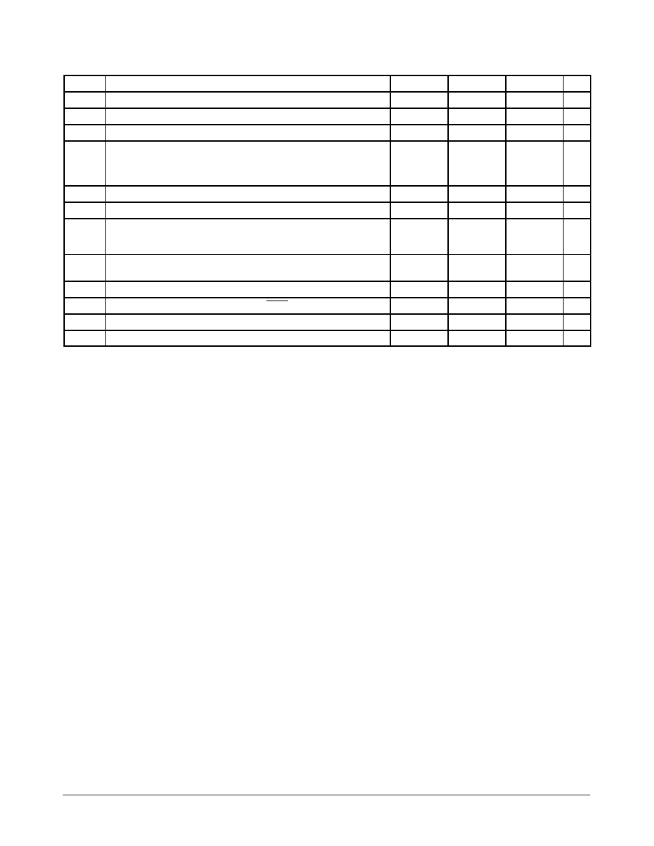
Figure 3. Output Disable / Enable Timing
CLKX
CLKX
OEX
QXn
QXn
50%
t
PDL
(OEX to QXn)
t
PLD
(OEX to QXn)
Outputs Disabled
Figure 4. Output Voltage Amplitude (V
OUTPP
) versus Clock Output Frequency at Ambient Temperature (Typical)
800
700
600
500
400
300
200
100
0
0
1
2
3
f
OUT
, CLOCK OUTPUT FREQUENCY (GHz)
V
OUTPP
, OUTPUT VOL
T
AGE
AMPLITUDE
(TYP)
Figure 5. Typical Termination for Output Driver and Device Evaluation
(See Application Note AND8020/D - Termination of ECL Logic Devices.)
Driver
Device
Receiver
Device
Q
D
Q
D
Z
o
= 50 W
Z
o
= 50 W
50 W
50 W
V
TT
V
TT
= V
CC
- 2.0 V
NB4L6254
http://onsemi.com
7
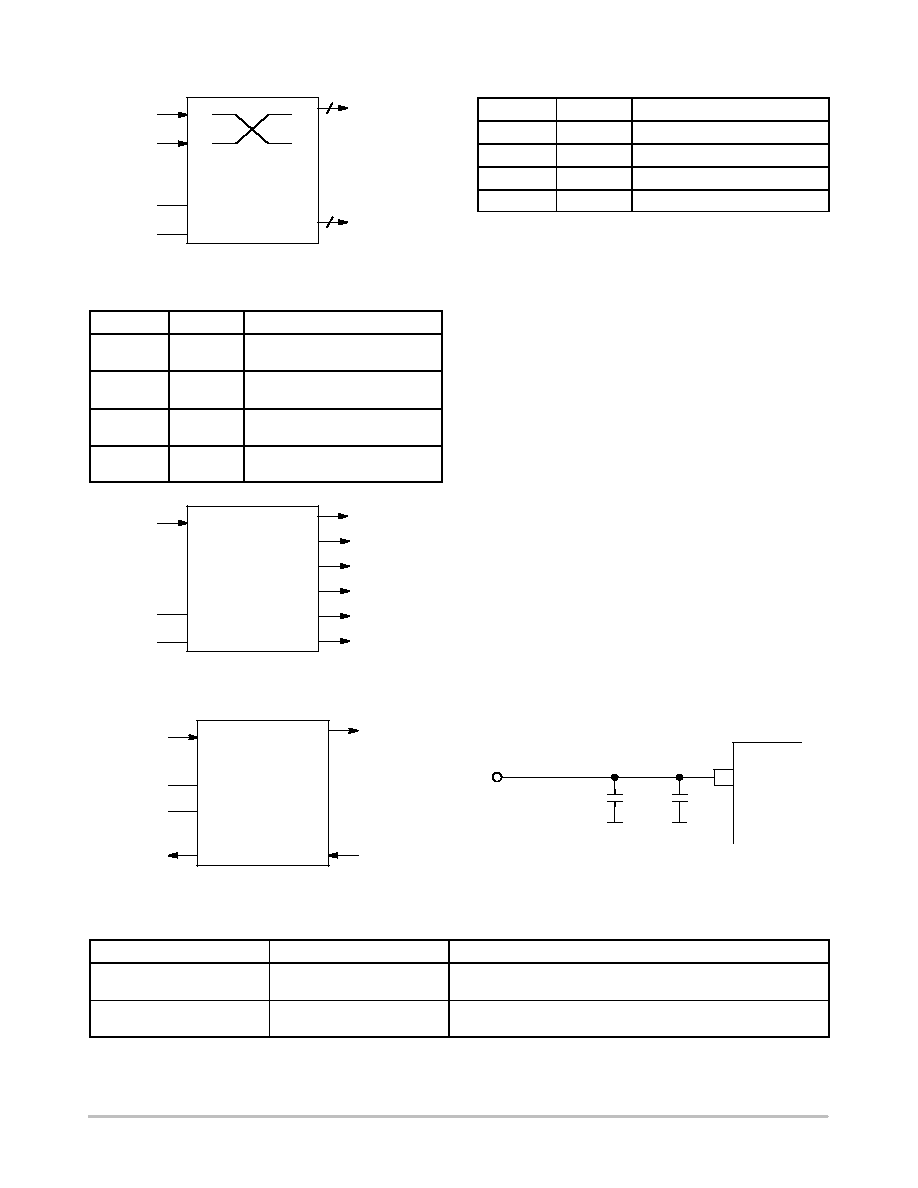
Example Configurations
Figure 6. 2 x 2 Clock Switch
CLK0
CLK1
SEL0
SEL1
System A
System B
3
3
SEL0
SEL1
Switch Configuration
0
0
CLK0 Clocks System A and
System B
0
1
CLK1 Clocks System A and
System B
1
0
CLK0 Clocks System A and CLK1
Clocks System B
1
1
CLK1 Clocks System B and CLK1
Clocks System A
Figure 7. 1:6 Clock Fanout Buffer
CLK0
CLK1
SEL0
SEL1
0
0
Figure 8. Loopback Device
System-Tx
CLK0
SEL0
SEL1
QBn
CLK1
Transmitter
QAn
System-Rx
Receiver
SEL0
SEL1
Switch Configuration
0
0
System Loopback
0
1
Line Loopback
1
0
Transmit/Receive Operation
1
1
System and Line Loopback
APPLICATIONS INFORMATION
Maintaining Lowest Device Skew
The NB4L6254 guarantees low output-output bank skew
at 50 ps and a part-to-part skew of 250 ps. To ensure low
skew clock signals in the application, both outputs of any
differential output pair need to be terminated identically,
even if only one output is used. When fewer than all nine
output pairs are used, identical termination of all output pairs
within the output bank is recommended. If an entire output
bank is not used, it is recommended to leave all of these
outputs open and unterminated. This will reduce the device
power consumption while maintaining minimum output
skew.
Power Supply Bypassing
The NB4L6254 is a mixed analog/digital product. The
differential architecture of the NB4L6254 supports low
noise signal operation at high frequencies. In order to
maintain its superior signal quality all V
CC
pins should be
bypassed by high-frequency ceramic capacitors connected
to GND. If the spectral frequencies of the internally
generated switching noise on the supply pins cross the series
resonant port of an individual bypass capacitor, its overall
impedance begins to look inductive and thus increases with
increasing frequency. The parallel capacitor combination
shown ensures that a low impedance path to ground exists
for frequencies well above the noise bandwidth.
Figure 9. V
CC
Power Supply Bypass
V
CC
NB4L6254
33...100 nF
0.1 nF
V
CC
ORDERING INFORMATION
Device
Package
Shipping
NB4L6254FAG
LQFP-32
(Pb-Free)
250 Units / Tray
NB4L6254FAR2G
LQFP-32
(Pb-Free)
2000 / Tape & Reel
For information on tape and reel specifications, including part orientation and tape sizes, please refer to our Tape and Reel Packaging
Specifications Brochure, BRD8011/D.
NB4L6254
http://onsemi.com
8
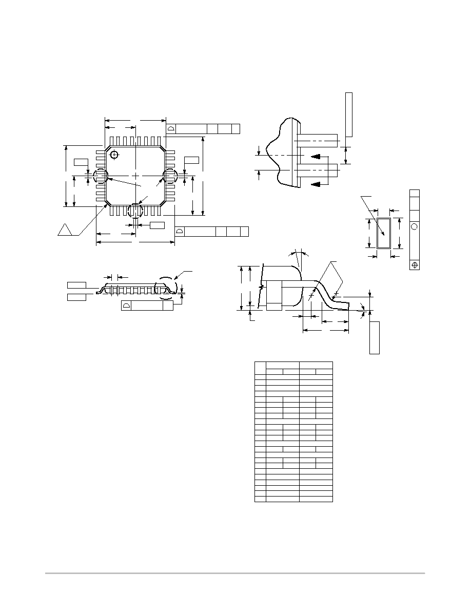
PACKAGE DIMENSIONS
ÉÉ
ÉÉ
ÉÉ
DETAIL Y
A
S1
V
B
1
8
9
17
25
32
AE
AE
P
DETAIL Y
BASE
N
J
D
F
METAL
SECTION AE-AE
G
SEATING
PLANE
R
Q
_
W
K
X
0.250 (0.010)
GAUGE PLANE
E
C
H
DETAIL AD
DETAIL AD
A1
B1
V1
4X
S
4X
9
-T-
-Z-
-U-
T-U
0.20 (0.008)
Z
AC
T-U
0.20 (0.008)
Z
AB
0.10 (0.004) AC
-AC-
-AB-
M
_
8X
-
T
-
,
-
U
-
,
-
Z
-
T-U
M
0.20 (0.008)
Z
AC
32 LEAD LQFP
CASE 873A-02
ISSUE C
NOTES:
1. DIMENSIONING AND TOLERANCING
PER ANSI Y14.5M, 1982.
2. CONTROLLING DIMENSION:
MILLIMETER.
3. DATUM PLANE -AB- IS LOCATED AT
BOTTOM OF LEAD AND IS COINCIDENT
WITH THE LEAD WHERE THE LEAD
EXITS THE PLASTIC BODY AT THE
BOTTOM OF THE PARTING LINE.
4. DATUMS -T-, -U-, AND -Z- TO BE
DETERMINED AT DATUM PLANE -AB-.
5. DIMENSIONS S AND V TO BE
DETERMINED AT SEATING PLANE -AC-.
6. DIMENSIONS A AND B DO NOT INCLUDE
MOLD PROTRUSION. ALLOWABLE
PROTRUSION IS 0.250 (0.010) PER SIDE.
DIMENSIONS A AND B DO INCLUDE
MOLD MISMATCH AND ARE
DETERMINED AT DATUM PLANE -AB-.
7. DIMENSION D DOES NOT INCLUDE
DAMBAR PROTRUSION. DAMBAR
PROTRUSION SHALL NOT CAUSE THE
D DIMENSION TO EXCEED 0.520 (0.020).
8. MINIMUM SOLDER PLATE THICKNESS
SHALL BE 0.0076 (0.0003).
9. EXACT SHAPE OF EACH CORNER MAY
VARY FROM DEPICTION.
DIM
A
MIN
MAX
MIN
MAX
INCHES
7.000 BSC
0.276 BSC
MILLIMETERS
B
7.000 BSC
0.276 BSC
C
1.400
1.600
0.055
0.063
D
0.300
0.450
0.012
0.018
E
1.350
1.450
0.053
0.057
F
0.300
0.400
0.012
0.016
G
0.800 BSC
0.031 BSC
H
0.050
0.150
0.002
0.006
J
0.090
0.200
0.004
0.008
K
0.450
0.750
0.018
0.030
M
12 REF
12 REF
N
0.090
0.160
0.004
0.006
P
0.400 BSC
0.016 BSC
Q
1
5
1
5
R
0.150
0.250
0.006
0.010
V
9.000 BSC
0.354 BSC
V1
4.500 BSC
0.177 BSC
_
_
_
_
_
_
B1
3.500 BSC
0.138 BSC
A1
3.500 BSC
0.138 BSC
S
9.000 BSC
0.354 BSC
S1
4.500 BSC
0.177 BSC
W
0.200 REF
0.008 REF
X
1.000 REF
0.039 REF
NB4L6254
http://onsemi.com
9
ON Semiconductor and are registered trademarks of Semiconductor Components Industries, LLC (SCILLC). SCILLC reserves the right to make changes without further notice
to any products herein. SCILLC makes no warranty, representation or guarantee regarding the suitability of its products for any particular purpose, nor does SCILLC assume any liability
arising out of the application or use of any product or circuit, and specifically disclaims any and all liability, including without limitation special, consequential or incidental damages.
"Typical" parameters which may be provided in SCILLC data sheets and/or specifications can and do vary in different applications and actual performance may vary over time. All
operating parameters, including "Typicals" must be validated for each customer application by customer's technical experts. SCILLC does not convey any license under its patent rights
nor the rights of others. SCILLC products are not designed, intended, or authorized for use as components in systems intended for surgical implant into the body, or other applications
intended to support or sustain life, or for any other application in which the failure of the SCILLC product could create a situation where personal injury or death may occur. Should
Buyer purchase or use SCILLC products for any such unintended or unauthorized application, Buyer shall indemnify and hold SCILLC and its officers, employees, subsidiaries, affiliates,
and distributors harmless against all claims, costs, damages, and expenses, and reasonable attorney fees arising out of, directly or indirectly, any claim of personal injury or death
associated with such unintended or unauthorized use, even if such claim alleges that SCILLC was negligent regarding the design or manufacture of the part. SCILLC is an Equal
Opportunity/Affirmative Action Employer. This literature is subject to all applicable copyright laws and is not for resale in any manner.
PUBLICATION ORDERING INFORMATION
N. American Technical Support: 800-282-9855 Toll Free
USA/Canada
Japan: ON Semiconductor, Japan Customer Focus Center
2-9-1 Kamimeguro, Meguro-ku, Tokyo, Japan 153-0051
Phone: 81-3-5773-3850
NB4L6254/D
ECLinPS is a trademark of Semiconductor Components INdustries, LLC (SCILLC).
LITERATURE FULFILLMENT:
Literature Distribution Center for ON Semiconductor
P.O. Box 5163, Denver, Colorado 80217 USA
Phone: 303-675-2175 or 800-344-3860 Toll Free USA/Canada
Fax: 303-675-2176 or 800-344-3867 Toll Free USA/Canada
Email: orderlit@onsemi.com
ON Semiconductor Website: http://onsemi.com
Order Literature: http://www.onsemi.com/litorder
For additional information, please contact your
local Sales Representative.