 | –≠–ª–µ–∫—Ç—Ä–æ–Ω–Ω—ã–π –∫–æ–º–ø–æ–Ω–µ–Ω—Ç: NB6L16DG | –°–∫–∞—á–∞—Ç—å:  PDF PDF  ZIP ZIP |
©
Semiconductor Components Industries, LLC, 2004
September, 2004 - Rev. 4
1
Publication Order Number:
NB6L16/D
NB6L16
2.5V / 3.3V Multilevel Input to
Differential LVPECL/LVNECL
Clock or Data
Receiver/Driver/Translator
Buffer
The NB6L16 is a high precision, low power ECL differential clock
or data receiver/driver/translator buffer. The device is functionally
equivalent to the EL16, EP16, LVEL16 and NBSG16 devices. With
output transition times of 70 ps, it is ideally suited for high frequency,
low power systems. The device is targeted for Backplane buffering,
GbE clock/data distribution, Fibre Channel distribution and SONET
clock/data distribution applications.
Input accept LVNECL (Negative ECL), LVPECL (Positive ECL),
LVTTL, LVCMOS, CML, or LVDS. Outputs are 800 mV
ECL signals.
The V
BB
pin, an internally generated voltage supply, is available to
this device only. For single-ended input conditions, the unused
differential input is connected to V
BB
as a switching reference voltage.
V
BB
may also rebias AC coupled inputs. When used, decouple V
BB
and V
CC
via a 0.01 mF capacitor and limit current sourcing or sinking
to 0.5 mA. When not used, V
BB
should be left open.
∑
Maximum Input Clock Frequency
w 6 GHz Typical
∑
Maximum Input Data Rate Frequency
w 6 Gb/s Typical
∑
Low 12 mA Typical Power Supply Current
∑
70 ps Typical Rise/Fall Times
∑
130 ps Input Propagation Delay
∑
On-Chip Reference for ECL Single-Ended Input - V
BB
Output
∑
PECL Mode Operating Range:
V
CC
= 2.375 V to 3.465 V with V
EE
= 0 V
∑
NECL Mode Operating Range:
V
CC
= 0 V with V
EE
= -2.375 V to -3.465 V
∑
Open Input Default State
∑
LVDS, LVPECL, LVNECL, LVCMOS, LVTTL and CML Input
Compatible
∑
Pb-Free Packages are Available
A
= Assembly Location
L
= Wafer Lot
Y
= Year
W
= Work Week
MARKING
DIAGRAMS*
ALYW
6L16
SOIC-8
D SUFFIX
CASE 751
1
8
TSSOP-8
DT SUFFIX
CASE 948R
1
8
1
8
*For additional marking information, refer to
Application Note AND8002/D.
6L16
ALYW
1
8
See detailed ordering and shipping information in the package
dimensions section on page 10 of this data sheet.
ORDERING INFORMATION
http://onsemi.com
http://onsemi.com

NB6L16
http://onsemi.com
2
1
2
3
4
5
6
7
8
Q
D
NC
Figure 1. Pinout (Top View) and Logic Diagram
V
BB
R2
R2
R1
R1
V
EE
Q
D
V
CC
Table 1. PIN DESCRIPTION
Pin
Name
I/O
Default State
Description
1
NC
-
-
No Connect. The NC pin is electrically connected to the die and MUST
be left open.
2
D
LVDS, CML, LVPECL,
LVNECL, LVTTL, LVCMOS
Input
LOW
Non-inverted differential clock/data input. Internal 75 k
W
to V
CC
and
37.5 k
W
to V
EE
.
3
D
LVDS, CML, LVPECL,
LVNECL, LVTTL, LVCMOS
Input
HIGH
Inverted differential clock/data input. Internal 37.5 k
W
to V
CC
and 75 k
W
to V
EE
.
4
V
BB
-
-
Internally generated ECL reference voltage supply.
5
V
EE
-
-
Negative power supply voltage.
6
Q
ECL Output
Inverted differential ECL output. Typically terminated with 50
W
resistor
to V
CC
≠ 2.0 V.
7
Q
ECL Output
Non-inverted differential ECL output. Typically terminated with 50
W
resistor to V
CC
≠ 2.0 V.
8
V
CC
-
-
Positive power supply voltage.
Table 2. ATTRIBUTES
Characteristics
Value
Internal Input Default State Resistor
(R1)
37.5 k
W
Internal Input Default State Resistor
(R2)
75 k
W
ESD Protection
Human Body Model
Machine Model
Charged Device Model
> 2 kV
> 100 V
> 1 kV
Moisture Sensitivity, Indefinite Time Out of Drypack (Note 1)
Level 1
Flammability Rating
Oxygen Index: 28 to 34
UL 94 V-0 @ 1.125 in
Transistor Count
167
Meets or exceeds JEDEC Spec EIA/JESD78 IC Latchup Test
1. For additional information, see Application Note AND8003/D.
NB6L16
http://onsemi.com
3
Table 3. MAXIMUM RATINGS
Symbol
Parameter
Condition 1
Condition 2
Rating
Unit
s
V
CC
PECL Mode Power Supply
V
EE
= 0 V
3.6
V
V
EE
NECL Mode Power Supply
V
CC
= 0 V
-3.6
V
V
I
PECL Mode Input Voltage
V
EE
= 0 V
V
I
v
V
CC
3.6
V
I
C
ode
u
o age
NECL Mode Input Voltage
EE
0
V
CC
= 0 V
I
CC
V
I
w
V
EE
3 6
-3.6
V
I
out
Output Current
Continuous
Surge
25
50
mA
mA
V
INPP
Differential Input Voltage
|D - D|
V
CC
- V
EE
w
2.8 V
V
CC
- V
EE
t
2.8 V
2.8
|V
CC
- V
EE
|
V
I
BB
V
BB
Sink/Source
±
0.5
mA
T
A
Operating Temperature Range
-40 to +85
∞
C
T
stg
Storage Temperature Range
-65 to +150
∞
C
q
JA
Thermal Resistance (Junction-to-Ambient)
0 lfpm
500 lfpm
SOIC-8
SOIC-8
190
130
∞
C/W
∞
C/W
q
JC
Thermal Resistance (Junction-to-Case)
Standard Board
SOIC-8
41 to 44
∞
C/W
q
JA
Thermal Resistance (Junction-to-Ambient)
0 lfpm
500 lfpm
TSSOP-8
TSSOP-8
185
140
∞
C/W
∞
C/W
q
JC
Thermal Resistance (Junction-to-Case)
Standard Board
TSSOP-8
41 to 44
∞
C/W
T
sol
Wave Solder
Standard
Pb-Free
v
3 sec @ 248
∞
C
v
3 sec @ 260
∞
C
265
265
∞
C
Maximum ratings are those values beyond which device damage can occur. Maximum ratings applied to the device are individual stress limit
values (not normal operating conditions) and are not valid simultaneously. If these limits are exceeded, device functional operation is not implied,
damage may occur and reliability may be affected.
NB6L16
http://onsemi.com
4
Table 4. DC CHARACTERISTICS, PECL
V
CC
= 2.5 V, V
EE
= 0 V (Note 4)
-40
∞
C
25
∞
C
85
∞
C
Symbol
Characteristic
Min
Typ
Max
Min
Typ
Max
Min
Typ
Max
Unit
I
EE
Negative Power Supply Current (Note 5)
10
12
18
10
12
18
10
12
18
mA
V
OH
Output HIGH Voltage (Note 6)
1350
1450
1550
1400
1500
1600
1450
1550
1650
mV
V
OL
Output LOW Voltage (Note 6)
565
725
870
630
765
920
690
825
970
mV
DIFFERENTIAL INPUT DRIVEN SINGLE-ENDED (Figures 10, 12)
V
th
Input Threshold Reference Voltage
Range (Notes 2, 7)
1125
V
CC
-75
1125
V
CC
-75
1125
V
CC
-75
mV
V
IH
Single-Ended Input HIGH Voltage
V
th
+75
V
CC
V
th
+75
V
CC
V
th
+75
V
CC
mV
V
IL
Single-Ended Input LOW Voltage
V
EE
V
th
-75
V
EE
V
th
-75
V
EE
V
th
-75
mV
DIFFERENTIAL INPUTS DRIVEN DIFFERENTIALLY (Figures 11, 13)
V
IHD
Differential Input HIGH Voltage
1200
V
CC
1200
V
CC
1200
V
CC
mV
V
ILD
Differential Input LOW Voltage
V
EE
V
CC
-75
V
EE
V
CC
-75
V
EE
V
CC
-75
mV
V
CMR
Input Common Mode Range
(Differential Cross-Point Voltage)
(Note 3)
1163
V
CC
-38
1163
V
CC
-38
1163
V
CC
-38
mV
V
ID
Differential Input Voltage (V
IHD
- V
ILD
)
75
2500
75
2500
75
2500
mV
I
IH
Input HIGH Current
D
D
50
10
150
150
50
10
150
150
50
10
150
150
m
A
I
IL
Input LOW Current
D
D
-150
-150
-5
-30
-150
-150
-5
-30
-150
-150
-5
-30
m
A
NOTE: Device will meet the specifications after thermal equilibrium has been established when mounted in a test socket or printed circuit
board with maintained transverse airflow greater than 500 lfpm. Electrical parameters are guaranteed only over the declared
operating temperature range. Functional operation of the device exceeding these conditions is not implied. Device specification limit
values are applied individually under normal operating conditions and not valid simultaneously.
2. V
th
is applied to the complementary input when operating in single-ended mode.
3. V
CMR
minimum varies 1:1 with V
EE
, V
CMR
maximum varies 1:1 with V
CC
.
4. Input and output parameters vary 1:1 with V
CC
. V
EE
can vary +0.125 V to -1.3 V.
5. All input and output pins left open.
6. All loading with 50
W
to V
CC
- 2.0 V.
7. Do not use V
BB
as a reference voltage for single-ended PECL signals when operating device at V
CC
- V
EE
< 3.0 V.
NB6L16
http://onsemi.com
5
Table 5. DC CHARACTERISTICS, PECL
V
CC
= 3.3 V, V
EE
= 0 V (Note 10)
-40
∞
C
25
∞
C
85
∞
C
Symbol
Characteristic
Min
Typ
Max
Min
Typ
Max
Min
Typ
Max
Unit
I
EE
Negative Power Supply Current (Note 11)
10
12
18
10
12
18
10
12
18
mA
V
OH
Output HIGH Voltage (Note 12)
2150
2250
2350
2200
2300
2400
2250
2350
2450
mV
V
OL
Output LOW Voltage (Note 12)
1365
1525
1670
1430
1565
1720
1490
1625
1770
mV
DIFFERENTIAL INPUT DRIVEN SINGLE-ENDED (Figures 10, 12)
V
th
Input Threshold Reference Voltage
Range (Note 8)
1125
V
CC
-75
1125
V
CC
-75
1125
V
CC
-75
mV
V
IH
Single-Ended Input HIGH Voltage
V
th
+75
V
CC
V
th
+75
V
CC
V
th
+75
V
CC
mV
V
IL
Single-Ended Input LOW Voltage
V
EE
V
th
-75
V
EE
V
th
-75
V
EE
V
th
-75
mV
V
BB
Output Voltage Reference
1880
1980
2070
1880
1980
2070
1880
1980
2070
mV
DIFFERENTIAL INPUTS DRIVEN DIFFERENTIALLY (Figures 11, 13)
V
IHD
Differential Input HIGH Voltage
1200
V
CC
1200
V
CC
1200
V
CC
mV
V
ILD
Differential Input LOW Voltage
V
EE
V
CC
-75
V
EE
V
CC
-75
V
EE
V
CC
-75
mV
V
CMR
Input Common Mode Range
(Differential Cross-Point Voltage)
(Note 9)
1163
V
CC
-38
1163
V
CC
-38
1163
V
CC
-38
mV
V
ID
Differential Input Voltage (V
IHD
- V
ILD
)
75
2500
75
2500
75
2500
mV
I
IH
Input HIGH Current
D
D
50
10
150
150
50
10
150
150
50
10
150
150
m
A
I
IL
Input LOW Current
D
D
-150
-150
-5
-30
-150
-150
-5
-30
-150
-150
-5
-30
m
A
NOTE: Device will meet the specifications after thermal equilibrium has been established when mounted in a test socket or printed circuit
board with maintained transverse airflow greater than 500 lfpm. Electrical parameters are guaranteed only over the declared
operating temperature range. Functional operation of the device exceeding these conditions is not implied. Device specification limit
values are applied individually under normal operating conditions and not valid simultaneously.
8. V
th
is applied to the complementary input when operating in single-ended mode.
9. V
CMR
minimum varies 1:1 with V
EE
, V
CMR
maximum varies 1:1 with V
CC
.
10. Input and output parameters vary 1:1 with V
CC
. V
EE
can vary +0.925 V to -0.5 V.
11. All input and output pins left open.
12. All loading with 50
W
to V
CC
- 2.0 V.

NB6L16
http://onsemi.com
6
Table 6. DC CHARACTERISTICS, NECL
V
CC
= 0 V, V
EE
= -3.465 V to -2.375 V (Note 15)
-40
∞
C
25
∞
C
85
∞
C
Symbol
Characteristic
Min
Typ
Max
Min
Typ
Max
Min
Typ
Max
Unit
I
EE
Negative Power Supply Current
(Note 17)
10
12
18
10
12
18
10
12
18
mA
V
OH
Output HIGH Voltage (Note 16)
-1150
-1050
-950
-1100
-1000
-900
-1050
-950
-850
mV
V
OL
Output LOW Voltage (Note 16)
-1935
-1775
-1630
-1870
-1735
-1580
-1810
-1675
-1530
mV
DIFFERENTIAL INPUT DRIVEN SINGLE-ENDED (Figures 10, 12)
V
th
Input Threshold Reference Voltage
Range (Note 8)
V
EE
+1125
V
CC
-75
V
EE
+1125
V
CC
-75
V
EE
+1125
V
CC
-75
mV
V
IH
Single-Ended Input HIGH Voltage
V
th
+75
V
CC
V
th
+75
V
CC
V
th
+75
V
CC
mV
V
IL
Single-Ended Input LOW Voltage
V
EE
V
th
-75
V
EE
V
th
-75
V
EE
V
th
-75
mV
V
BB
Output Voltage Reference
-1420
-1320
-1230
-1420
-1320
-1230
-1420
-1320
-1230
mV
DIFFERENTIAL INPUTS DRIVEN DIFFERENTIALLY (Figures 11, 13)
V
IHD
Differential Input HIGH Voltage
V
EE
+
1200
V
CC
V
EE
+
1200
V
CC
V
EE
+
1200
V
CC
mV
V
ILD
Differential Input LOW Voltage
V
EE
V
CC
-75
V
EE
V
CC
-75
V
EE
V
CC
-75
mV
V
CMR
Input Common Mode Range
(Differential Cross-Point Voltage)
(Note 9)
V
EE
+
1163
V
CC
-38
V
EE
+
1163
V
CC
-38
V
EE
+
1163
V
CC
-38
mV
V
ID
Differential Input Voltage (V
IHD
- V
ILD
)
75
2500
75
2500
75
2500
mV
I
IH
Input HIGH Current
D
D
50
10
150
150
50
10
150
150
50
10
150
150
m
A
I
IL
Input LOW Current
D
D
-150
-150
-5
-30
-150
-150
-5
-30
-150
-150
-5
-30
m
A
NOTE: Device will meet the specifications after thermal equilibrium has been established when mounted in a test socket or printed circuit
board with maintained transverse airflow greater than 500 lfpm. Electrical parameters are guaranteed only over the declared
operating temperature range. Functional operation of the device exceeding these conditions is not implied. Device specification limit
values are applied individually under normal operating conditions and not valid simultaneously.
13. V
th
is applied to the complementary input when operating in single-ended mode.
14. V
CMR
minimum varies 1:1 with V
EE
, V
CMR
maximum varies 1:1 with V
CC
.
15. Input and output parameters vary 1:1 with V
CC
.
16. All loading with 50
W
to V
CC
- 2.0 V.
17. All input and output pins left open.
NB6L16
http://onsemi.com
7
Table 7. AC CHARACTERISTICS
V
CC
= 0 V; V
EE
= -3.465 V to -2.375 V or V
CC
= 2.375 V to 3.465 V; V
EE
= 0 V (Note 18)
-40
∞
C
25
∞
C
85
∞
C
Symbol
Characteristic
Min
Typ
Max
Min
Typ
Max
Min
Typ
Max
Unit
V
OUTPP
Output Voltage Amplitude
f
in
< 3 GHz
(See Figures 2 & 3)
f
in
< 6 GHz
500
270
700
350
500
270
700
350
500
270
700
300
mV
t
PLH
,
t
PHL
Propagation Delay to
Output Differential @ 1 GHz
80
130
180
80
130
180
85
135
185
ps
t
SKEW
Duty Cycle Skew (Note 19)
Device-to-Device Skew
3
30
25
60
3
30
25
60
3
30
25
60
ps
t
JITTER
RMS Random Clock Jitter
(Note 20)
f
in
< 6 GHz
Peak-to-Peak Data Dependent JItter
(Note 21)
f
in
< 6 Gb/s
0.2
2
1
12
0.2
2
1
12
0.2
2
1
12
ps
V
INPP
Input Voltage Swing / Sensitivity
(Differential Configuration) (Note 22)
75
700
2500
75
700
2500
75
700
2500
mV
t
r
t
f
Output Rise/Fall Times
Q, Q
(20% - 80%)
30
70
120
30
70
120
30
70
120
ps
NOTE: Device will meet the specifications after thermal equilibrium has been established when mounted in a test socket or printed circuit
board with maintained transverse airflow greater than 500 lfpm. Electrical parameters are guaranteed only over the declared
operating temperature range. Functional operation of the device exceeding these conditions is not implied. Device specification limit
values are applied individually under normal operating conditions and not valid simultaneously.
18. Measured using a 800 mV source, 50% duty cycle clock source. All loading with 50
W
to V
CC
. Input edge rates 40 ps (20% - 80%).
19. See Figure 9 t
skew
= |t
PLH
- t
PHL
| for a nominal 50% differential clock input waveform. Skew is measured between outputs under identical
transitions and conditions @ 1 GHz.
20. Additive RMS jitter with 50% duty cycle clock signal at 6 GHz.
21. Additive Peak-to-Peak data dependent jitter with NRZ PRBS 2
23
-1 data rate at 6 Gb/s.
22. V
INPP(max)
cannot exceed V
CC
- V
EE
. (Applicable only when V
CC
- V
EE
< 2500 mV). Input voltage swing is a single-ended measurement
operating in the differential mode.
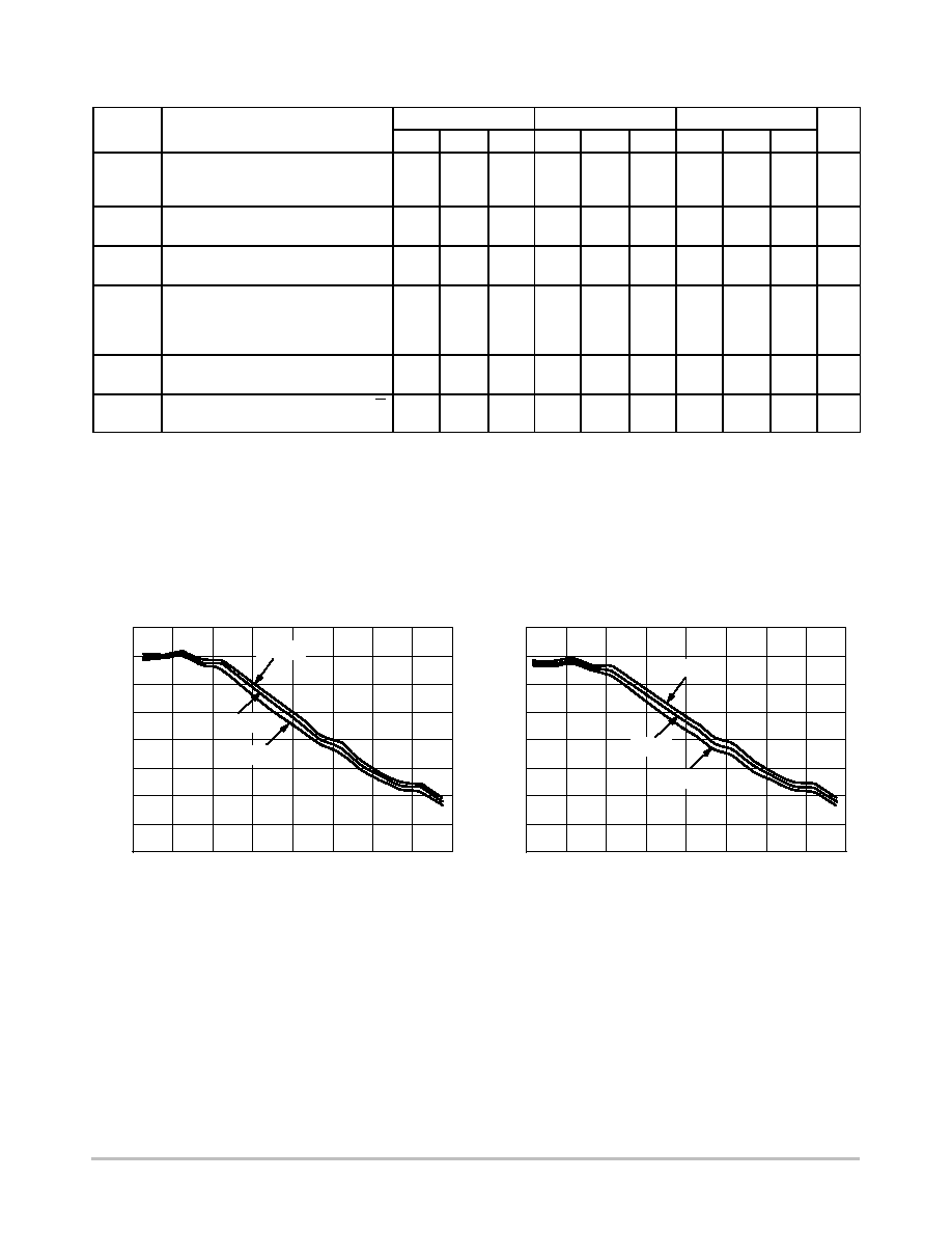
0.0
0.1
0.2
0.3
0.4
0.5
0.6
0.7
0.8
1
2
3
4
5
6
7
8
OUTPUT
VOL
T
AGE
AMPLITUDE (V)
INPUT CLOCK FREQUENCY (GHz)
Figure 2. Output Voltage Amplitude (V
OUTPP
)
versus Input Clock Frequency (f
IN
) and
Temperature at V
CC
- V
EE
= 3.3 V
0.0
0.1
0.2
0.3
0.4
0.5
0.6
0.7
0.8
1
2
3
4
5
6
7
8
INPUT CLOCK FREQUENCY (GHz)
Figure 3. Output Voltage Amplitude (V
OUTPP
)
versus Input Clock Frequency (f
IN
) and
Temperature at V
CC
- V
EE
= 2.5 V
OUTPUT
VOL
T
AGE
AMPLITUDE (V)
85
∞
C
-40
∞
C
25
∞
C
-40
∞
C
25
∞
C
85
∞
C
NB6L16
http://onsemi.com
8
OUTPUT
VOL
T
AGE
AMPLITUDE (100 mV/div)
TIME (62 ps/div)
Figure 4. Typical Output Waveform at
2.488 Gb/s with PRBS 2
23
-1 (Total System
Pk-Pk Jitter is 16 ps. Device Pk-Pk Jitter
Contribution is 3 ps)
OUTPUT
VOL
T
AGE
AMPLITUDE (100 mV/div)
TIME (32 ps/div)
Figure 5. Typical Output Waveform at
6.125 Gb/s with PRBS 2
23
-1 (Total System
Pk-Pk Jitter is 17 ps. Device Pk-Pk Jitter
Contribution is 4 ps)
NOTE:
V
CC
- V
EE
= 3.3 V; V
IN
= 700 mV; T
A
= 25
∞
C.
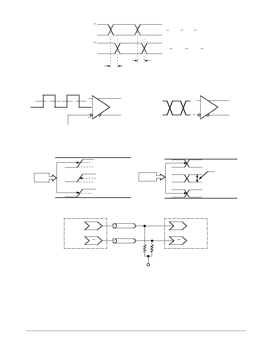
80
90
100
110
120
130
140
150
160
170
180
190
2.375
2.5
3.3
3.465
PROP
AGA
TION DELA
YS (ps)
POWER SUPPLY VOLTAGE (V)
Figure 6. Propagation Delay versus Power
Supply Voltage and Temperature
30
40
50
60
70
80
90
100
110
120
2.375
2.5
3.3
3.465
RISE/F
ALL
TIME
(ps)
POWER SUPPLY VOLTAGE (V)
Figure 7. Rise/Fall Time versus Power Supply
Voltage and Temperature
10
11
12
13
14
15
16
17
18
-40
25
85
Figure 8. I
EE
Current versus Temperature and
Power Supply Voltage
TEMPERATURE (
∞
C)
I
EE
CURRENT (mA)
85
∞
C
-40
∞
C
25
∞
C
-40
∞
C
25
∞
C
85
∞
C
V
CC
- V
EE
= -3.465 V
V
CC
- V
EE
= -2.375 V
NB6L16
http://onsemi.com
9
Figure 9. AC Reference Measurement
D
D
Q
Q
t
PHL
t
PLH
V
INPP
(D) = V
IH
(D) - V
IL
(D)
V
INPP
(D) = V
IH
(D) - V
IL
(D)
V
OUTPP
(Q) = V
OH
(Q) - V
OL
(Q)
V
OUTPP
(Q) = V
OH
(Q) - V
OL
(Q)
D
V
th
D
V
th
Figure 10. Differential Input Driven
Single-Ended
D
D
Figure 11. Differential Inputs Driven
Differentially
V
IHmax
V
ILmax
V
IHTYP
V
thTYP
V
ILTYP
V
IHmin
V
ILmin
V
CC
V
thmax
V
thmin
GND
V
th
V
IHDmax
V
ILDmax
V
IHDmin
V
ILDmin
V
IHDtyp
V
ILDtyp
V
ID
= V
IHD
- V
ILD
V
CMR
V
CC
V
CMmax
V
CMmax
GND
Figure 12. V
th
Diagram
Figure 13. V
CMR
Diagram
Figure 14. Typical Termination for Output Driver and Device Evaluation
(See Application Note AND8020/D - Termination of ECL Logic Devices.)
Driver
Device
Receiver
Device
Q
D
Q
D
Z
o
= 50
W
Z
o
= 50
W
50
W
50
W
V
TT
V
TT
= V
CC
- 2.0 V

NB6L16
http://onsemi.com
10
ORDERING INFORMATION
Device
Package
Shipping
NB6L16D
SO-8
98 Units / Rail
NB6L16DG
SO-8
(Pb-Free)
98 Units / Rail
NB6L16DR2
SO-8
2500 / Tape & Reel
NB6L16DR2G
SO-8
(Pb-Free)
2500 / Tape & Reel
NB6L16DT
TSSOP-8
100 Units / Rail
NB6L16DTG*
TSSOP-8
(Pb-Free)
100 Units / Rail
NB6L16DTR2
TSSOP-8
2500 / Tape & Reel
NB6L16DTR2G*
TSSOP-8
(Pb-Free)
2500 / Tape & Reel
For information on tape and reel specifications, including part orientation and tape sizes, please refer to our Tape and Reel Packaging
Specifications Brochure, BRD8011/D.
*Future Product - Contact factory for availability.
Resource Reference of Application Notes
AN1405/D
- ECL Clock Distribution Techniques
AN1406/D
- Designing with PECL (ECL at +5.0 V)
AN1503/D
- ECLinPS
t
I/O SPiCE Modeling Kit
AN1504/D
- Metastability and the ECLinPS Family
AN1568/D
- Interfacing Between LVDS and ECL
AN1642/D
- The ECL Translator Guide
AND8001/D
- Odd Number Counters Design
AND8002/D
- Marking and Date Codes
AND8020/D
- Termination of ECL Logic Devices
AND8066/D
- Interfacing with ECLinPS
AND8090/D
- AC Characteristics of ECL Devices
NB6L16
http://onsemi.com
11
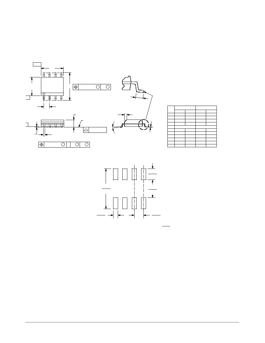
PACKAGE DIMENSIONS
SOIC-8
D SUFFIX
PLASTIC SOIC PACKAGE
CASE 751-07
ISSUE AC
1.52
0.060
7.0
0.275
0.6
0.024
1.270
0.050
4.0
0.155
mm
inches
SCALE 6:1
SEATING
PLANE
1
4
5
8
N
J
X 45
_
K
NOTES:
1. DIMENSIONING AND TOLERANCING PER
ANSI Y14.5M, 1982.
2. CONTROLLING DIMENSION: MILLIMETER.
3. DIMENSION A AND B DO NOT INCLUDE
MOLD PROTRUSION.
4. MAXIMUM MOLD PROTRUSION 0.15 (0.006)
PER SIDE.
5. DIMENSION D DOES NOT INCLUDE DAMBAR
PROTRUSION. ALLOWABLE DAMBAR
PROTRUSION SHALL BE 0.127 (0.005) TOTAL
IN EXCESS OF THE D DIMENSION AT
MAXIMUM MATERIAL CONDITION.
6. 751-01 THRU 751-06 ARE OBSOLETE. NEW
STANDARD IS 751-07.
A
B
S
D
H
C
0.10 (0.004)
DIM
A
MIN
MAX
MIN
MAX
INCHES
4.80
5.00
0.189
0.197
MILLIMETERS
B
3.80
4.00
0.150
0.157
C
1.35
1.75
0.053
0.069
D
0.33
0.51
0.013
0.020
G
1.27 BSC
0.050 BSC
H
0.10
0.25
0.004
0.010
J
0.19
0.25
0.007
0.010
K
0.40
1.27
0.016
0.050
M
0
8
0
8
N
0.25
0.50
0.010
0.020
S
5.80
6.20
0.228
0.244
-X-
Y-
G
M
Y
M
0.25 (0.010)
-
Y
M
0.25 (0.010)
Z
S
X
S
M
_
_
_
_
*For additional information on our Pb-Free strategy and soldering
details, please download the ON Semiconductor Soldering and
Mounting Techniques Reference Manual, SOLDERRM/D.
SOLDERING FOOTPRINT*
NB6L16
http://onsemi.com
12
PACKAGE DIMENSIONS
TSSOP-8
DT SUFFIX
PLASTIC TSSOP PACKAGE
CASE 948R-02
ISSUE A
DIM
MIN
MAX
MIN
MAX
INCHES
MILLIMETERS
A
2.90
3.10
0.114
0.122
B
2.90
3.10
0.114
0.122
C
0.80
1.10
0.031
0.043
D
0.05
0.15
0.002
0.006
F
0.40
0.70
0.016
0.028
G
0.65 BSC
0.026 BSC
L
4.90 BSC
0.193 BSC
M
0
6
0
6
_
_
_
_
SEATING
PLANE
PIN 1
1
4
8
5
DETAIL E
B
C
D
A
G
DETAIL E
F
M
L
2X
L/2
-U-
S
U
0.15 (0.006) T
S
U
0.15 (0.006) T
S
U
M
0.10 (0.004)
V
S
T
0.10 (0.004)
-T-
-V-
-W-
0.25 (0.010)
8x REF
K
IDENT
K
0.25
0.40
0.010
0.016
NOTES:
1. DIMENSIONING AND TOLERANCING PER ANSI
Y14.5M, 1982.
2. CONTROLLING DIMENSION: MILLIMETER.
3. DIMENSION A DOES NOT INCLUDE MOLD FLASH.
PROTRUSIONS OR GATE BURRS. MOLD FLASH
OR GATE BURRS SHALL NOT EXCEED 0.15
(0.006) PER SIDE.
4. DIMENSION B DOES NOT INCLUDE INTERLEAD
FLASH OR PROTRUSION. INTERLEAD FLASH OR
PROTRUSION SHALL NOT EXCEED 0.25 (0.010)
PER SIDE.
5. TERMINAL NUMBERS ARE SHOWN FOR
REFERENCE ONLY.
6. DIMENSION A AND B ARE TO BE DETERMINED
AT DATUM PLANE -W-.
ON Semiconductor and are registered trademarks of Semiconductor Components Industries, LLC (SCILLC). SCILLC reserves the right to make changes without further notice
to any products herein. SCILLC makes no warranty, representation or guarantee regarding the suitability of its products for any particular purpose, nor does SCILLC assume any liability
arising out of the application or use of any product or circuit, and specifically disclaims any and all liability, including without limitation special, consequential or incidental damages.
"Typical" parameters which may be provided in SCILLC data sheets and/or specifications can and do vary in different applications and actual performance may vary over time. All
operating parameters, including "Typicals" must be validated for each customer application by customer's technical experts. SCILLC does not convey any license under its patent rights
nor the rights of others. SCILLC products are not designed, intended, or authorized for use as components in systems intended for surgical implant into the body, or other applications
intended to support or sustain life, or for any other application in which the failure of the SCILLC product could create a situation where personal injury or death may occur. Should
Buyer purchase or use SCILLC products for any such unintended or unauthorized application, Buyer shall indemnify and hold SCILLC and its officers, employees, subsidiaries, affiliates,
and distributors harmless against all claims, costs, damages, and expenses, and reasonable attorney fees arising out of, directly or indirectly, any claim of personal injury or death
associated with such unintended or unauthorized use, even if such claim alleges that SCILLC was negligent regarding the design or manufacture of the part. SCILLC is an Equal
Opportunity/Affirmative Action Employer. This literature is subject to all applicable copyright laws and is not for resale in any manner.
PUBLICATION ORDERING INFORMATION
N. American Technical Support: 800-282-9855 Toll Free
USA/Canada
Japan: ON Semiconductor, Japan Customer Focus Center
2-9-1 Kamimeguro, Meguro-ku, Tokyo, Japan 153-0051
Phone: 81-3-5773-3850
NB6L16/D
ECLinPS is a trademark of Semiconductor Components Industries, LLC.
LITERATURE FULFILLMENT:
Literature Distribution Center for ON Semiconductor
P.O. Box 61312, Phoenix, Arizona 85082-1312 USA
Phone: 480-829-7710 or 800-344-3860 Toll Free USA/Canada
Fax: 480-829-7709 or 800-344-3867 Toll Free USA/Canada
Email: orderlit@onsemi.com
ON Semiconductor Website: http://onsemi.com
Order Literature: http://www.onsemi.com/litorder
For additional information, please contact your
local Sales Representative.