 | –≠–ª–µ–∫—Ç—Ä–æ–Ω–Ω—ã–π –∫–æ–º–ø–æ–Ω–µ–Ω—Ç: NB7L11MMN | –°–∫–∞—á–∞—Ç—å:  PDF PDF  ZIP ZIP |
©
Semiconductor Components Industries, LLC, 2005
February, 2005 - Rev. 0
1
Publication Order Number:
NB7L11M/D
NB7L11M
2.5V/3.3V Differential 1:2
Clock/Data Fanout Buffer/
Translator with CML
Outputs and Internal
Termination
The NB7L11M is a differential 1-to-2 clock/data distribution chip
with internal source termination and CML output structure, optimized
for low skew and minimal jitter. The device is functionally equivalent to
the EP11, LVEP11, or SG11 devices. Device produces two identical
output copies of clock or data operating up to 8 GHz or 12 Gb/s,
respectively. As such, NB7L11M is ideal for SONET, GigE, Fiber
Channel, Backplane and other clock/data distribution applications.
Inputs incorporate internal 50
W termination resistors and accept
LVPECL, CML, LVCMOS, LVTTL, or LVDS (See Table 6).
Differential 16 mA CML output provides matching internal 50
W
terminations, and 400 mV output swings when externally terminated,
50
W to V
CC
(See Figure 14).
The device is offered in a low profile 3x3 mm 16-pin QFN package.
Application notes, models, and support documentation are available at
www.onsemi.com.
∑
Maximum Input Clock Frequency up to 8 GHz Typical
∑
Maximum Input Data Rate up to 12 Gb/s Typical
∑
< 0.5 ps of RMS Clock Jitter
∑
< 10 ps of Data Dependent Jitter
∑
30 ps Typical Rise and Fall Times
∑
110 ps Typical Propagation Delay
∑
3 ps Typical Within Device Skew
∑
Operating Range: V
CC
= 2.375 V to 3.465 V with V
EE
= 0 V
∑
CML Output Level (400 mV Peak-to-Peak Output) Differential
Output Only
∑
50
W Internal Input and Output Termination Resistors
∑
Functionally Compatible with Existing 2.5 V/3.3 V LVEL, LVEP, EP
and SG Devices
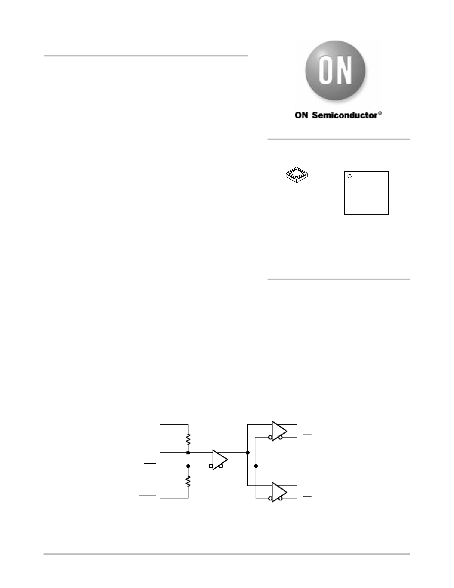
Figure 1. Logic Diagram
Q0
Q0
Q1
Q1
V
TCLK
CLK
CLK
V
TCLK
50
W
50
W
*For additional marking information, refer to
Application Note AND8002/D.
MARKING
DIAGRAM*
A = Assembly Location
L = Wafer Lot
Y = Year
W = Work Week
QFN-16
MN SUFFIX
CASE 485G
http://onsemi.com
16
NB7L
11M
ALYW
1
See detailed ordering and shipping information in the package
dimensions section on page 11 of this data sheet.
ORDERING INFORMATION

NB7L11M
http://onsemi.com
2
V
CC
Q1
Q1
V
CC
V
CC
Q0
Q0
V
CC
V
EE
V
EE
V
EE
V
EE
V
TCLK
CLK
CLK
V
TCLK
5
6
7
8
16
15
14
13
12
11
10
9
1
2
3
4
NB7L11M
Exposed Pad (EP)
Figure 2. QFN-16 Pinout (Top View)
Table 1. PIN DESCRIPTION
Pin
Name
I/O
Description
1
V
TCLK
-
Internal 50
W
Termination Pin for CLK
2
CLK
LVPECL, CML,
LVCMOS, LVTTL,
LVDS
Inverted Differential Clock/Data Input. (Note 1)
3
CLK
LVPECL, CML,
LVCMOS, LVTTL,
LVDS
Noninverted Differential Clock/Data Input. (Note 1)
4
V
TCLK
-
Internal 50
W
Termination Pin for CLK
5,8,13,16
V
CC
-
Positive Supply Voltage. All V
CC
pins must be externally connected to a Power Supply
to guarantee proper operation.
6
Q1
CML Output
Inverted CLK output 1 with internal 50
W
source termination resistor. (Note 2)
7
Q1
CML Output
Noninverted CLK output 1 with internal 50
W
source termination resistor. (Note 2)
9,10,11,12
V
EE
-
Negative Supply Voltage. All V
EE
pins must be externally connected to a Power Supply
to guarantee proper operation.
14
Q0
CML Output
Inverted CLK output 0 with internal 50
W
source termination resistor. (Note 2)
15
Q0
CML Output
Noninverted CLK output 0 with internal 50
W
source termination resistor. (Note 2)
-
EP
-
Exposed Pad. The thermally exposed pad on package bottom (see case drawing) must
be attached to a heatsinking conduit. It is recommended to connect the EP to the lower
potential (V
EE
).
1. In the differential configuration when the input termination pins (V
TCLK
, V
TCLK
) are connected to a common termination voltage or left open,
and if no signal is applied on CLK and CLK then the device will be susceptible to self-oscillation.
2. CML outputs require 50
W
receiver termination resistor to V
CC
for proper operation.

NB7L11M
http://onsemi.com
3
Table 2. ATTRIBUTES
Characteristics
Value
ESD Protection
Human Body Model
Machine Model
Charged Device Model
> 1500 V
> 50 V
> 500 V
Moisture Sensitivity (Note 3)
QFN-16
Level 1
Flammability Rating
Oxygen Index: 28 to 34
UL 94 V-0 @ 0.125 in
Transistor Count
285
Meets or exceeds JEDEC Spec EIA/JESD78 IC Latchup Test
3. For additional information, see Application Note AND8003/D.
Table 3. MAXIMUM RATINGS
Symbol
Parameter
Condition 1
Condition 2
Rating
Units
V
CC
Positive Power Supply
V
EE
= 0 V
3.6
V
V
I
Input Voltage
V
EE
= 0 V
V
EE
v
V
I
v
V
CC
3.6
V
V
INPP
Differential Input Voltage |CLK - CLK|
V
CC
- V
EE
w
2.8 V
V
CC
- V
EE
< 2.8 V
2.8
|V
CC
- V
EE
|
V
I
IN
Input Current Through R
T
(50
W
Resistor)
Static
Surge
45
80
mA
mA
I
out
Output Current
Continuous
Surge
25
50
mA
mA
T
A
Operating Temperature Range
QFN-16
-40 to +85
∞
C
T
stg
Storage Temperature Range
-65 to +150
∞
C
q
JA
Thermal Resistance (Junction-to-Ambient)
(Note 4)
0 lfpm
500 lfpm
QFN-16
QFN-16
42
36
∞
C/W
∞
C/W
q
JC
Thermal Resistance (Junction-to-Case)
2S2P (Note 4)
QFN-16
3 to 4
∞
C/W
T
sol
Wave Solder
Pb
Pb-Free
< 3 Sec @ 248
∞
C
< 3 Sec @ 260
∞
C
265
265
∞
C
Maximum ratings are those values beyond which device damage can occur. Maximum ratings applied to the device are individual stress limit
values (not normal operating conditions) and are not valid simultaneously. If these limits are exceeded, device functional operation is not implied,
damage may occur and reliability may be affected.
4. JEDEC standard multilayer board - 2S2P (2 signal, 2 power).
NB7L11M
http://onsemi.com
4
Table 4. DC CHARACTERISTICS, CLOCK Inputs, CML Outputs (
V
CC
= 2.375 V to 3.465 V, V
EE
= 0 V, T
A
= -40
∞
C to +85
∞
C)
(Note 5)
Symbol
Characteristic
Min
Typ
Max
Unit
I
CC
Power Supply Current (Input and Outputs open)
85
105
mA
V
OH
Output HIGH Voltage (Note 6)
V
CC
- 60
V
CC
- 20
V
CC
mV
V
OL
Output LOW Voltage (Note 6)
V
CC
- 530
V
CC
- 420
V
CC
- 360
mV
Differential Input Driven Single-Ended (see Figures 10 & 12) (Note 8)
V
th
Input Threshold Reference Voltage Range (Note 7)
1125
V
CC
- 75
mV
V
IH
Single-ended Input HIGH Voltage (Note 8)
V
th
+ 75
V
CC
mV
V
IL
Single-ended Input LOW Voltage (Note 8)
V
EE
V
th
- 75
mV
Differential Inputs Driven Differentially (see Figures 11 & 13) (Note 8)
V
IHCLK
Differential Input HIGH Voltage
1200
V
CC
mV
V
ILCLK
Differential Input LOW Voltage
V
EE
V
CC
- 75
mV
V
CMR
Input Common Mode Range (Differential Configuration)
1163
V
CC
≠ 38
mV
V
ID
Differential Input Voltage (V
IHCLK -
V
ILCLK
)
75
2500
mV
I
IH
Input HIGH Current CLK / CLK (V
TCLK
/V
TCLK
Open)
0
25
100
m
A
I
IL
Input LOW Current CLK / CLK (V
TCLK
/V
TCLK
Open)
-10
0
10
m
A
R
TIN
Internal Input Termination Resistor
45
50
55
W
R
TOUT
Internal Output Termination Resistor
45
50
55
W
R
Temp Coef
Internal I/O Termination Resistor Temperature Coefficient
6.38
m
W
/
∞
C
NOTE: Device will meet the specifications after thermal equilibrium has been established when mounted in a test socket or printed circuit board
with maintained airflow greater than 500 lfpm. Electrical parameters are guaranteed only over the declared operating temperature range.
Functional operation of the device exceeding these conditions is not implied. Device specification limit values are applied individually
under normal operating conditions and not valid simultaneously.
5. Input and output parameters vary 1:1 with V
CC
.
6. CML outputs require 50
W
receiver termination resistors to V
CC
for proper operation.
7. V
th
is applied to the complementary input when operating in single-ended mode.
8. V
CMR
min varies 1:1 with V
EE
, V
CMR
max varies 1:1 with V
CC
.
NB7L11M
http://onsemi.com
5
Table 5. AC CHARACTERISTICS
(V
CC
= 2.375 V to 3.465 V, V
EE
= 0 V; Note 9)
Symbol
Characteristic
-40
_
C
25
_
C
85
_
C
Unit
Min
Typ
Max
Min
Typ
Max
Min
Typ
Max
V
OUTPP
Output Voltage Amplitude (@V
INPPmin
) f
in
6 GHz
(See Figure 3)
f
in
8 GHz
280
140
400
300
280
140
400
300
280
140
400
300
mV
f
data
Maximum Operating Data Rate
10
12
10
12
10
12
Gb/s
t
PLH
,
t
PHL
Propagation Delay to Output Differential
70
110
150
70
110
150
70
110
150
ps
t
SKEW
Duty Cycle Skew (Note 10)
Within-Device Skew
Device-to-Device Skew (Note 11)
2.0
3.0
20
5.0
15
50
2.0
3.0
20
5.0
15
50
2.0
3.0
20
5.0
15
50
ps
t
JITTER
RMS Random Clock Jitter (Note 12)
f
in
= 6 GHz
f
in
=8 GHz
Peak/Peak Data Dependent Jitter f
in
= 2.488 Gb/s
(Note 13)
f
data
=5 Gb/s
f
data
=10 Gb/s
0.2
0.2
2.0
3.0
5.0
0.5
0.5
5.0
8.0
10
0.2
0.2
2.0
3.0
5.0
0.5
0.5
5.0
8.0
10
0.2
0.2
2.0
3.0
5.0
0.5
0.5
5.0
8.0
10
ps
V
INPP
Input Voltage Swing/Sensitivity
(Differential Configuration) (Note 14)
75
400
2500
75
400
2500
75
400
2500
mV
t
r
t
f
Output Rise/Fall Times @ 1 GHz
Q, Q
(20% - 80%)
30
60
30
60
30
60
ps
NOTE: Device will meet the specifications after thermal equilibrium has been established when mounted in a test socket or printed circuit board
with maintained airflow greater than 500 lfpm. Electrical parameters are guaranteed only over the declared operating temperature range.
Functional operation of the device exceeding these conditions is not implied. Device specification limit values are applied individually
under normal operating conditions and not valid simultaneously.
9. Measured by forcing V
INPP
(TYP) from a 50% duty cycle clock source. All loading with an external R
L
= 50
W
to V
CC
.
Input edge rates 40 ps (20% - 80%).
10. Duty cycle skew is measured between differential outputs using the deviations of the sum of Tpw- and Tpw+ @1 GHz.
11. Device to device skew is measured between outputs under identical transition @ 1 GHz.
12. Additive RMS jitter with 50% duty cycle clock signal at 8 GHz & 10 GHz.
13. Additive peak-to-peak data dependent jitter with input NRZ data at PRBS 2
^23
-1.
14. V
INPP
(MAX) cannot exceed V
CC
- V
EE
. Input voltage swing is a single-ended measurement operating in differential mode.
Figure 3. Output Voltage Amplitude (V
OUTPP
) versus
Input Clock Frequency (f
in
) at Ambient Temperature (Typical)
(V
INPP
= 400 mV)
INPUT FREQUENCY (GHz)
OUTPUT VOL
T
AGE AMPLITUDE
(mV)
500
400
300
200
100
0
12
11
10
9
8
7
6
5
4
3
2
1
0
V
CC
= 3.3 V
V
CC
= 2.5 V
NB7L11M
http://onsemi.com
6
Figure 4. Typical Output Waveform at 2.488 Gb/s
with PRBS 2
^23
-1 (V
inpp
= 75 mV)
Figure 5. Typical Output Waveform at 5 Gb/s
with PRBS 2
^23
-1 (V
inpp
= 75 mV)
Figure 6. Typical Output Waveform at 10.7 Gb/s
with PRBS 2
^23
-1 (V
inpp
= 75 mV)
Figure 7. Typical Output Waveform at 12 Gb/s
with PRBS 2
^23
-1 (V
inpp
= 75 mV)
Time (80.4 ps/div)
Time (40 ps/div)
Time (18.6 ps/div)
Time (18.2 ps/div)
V
oltage (50 mV/div)
V
oltage (50 mV/div)
V
oltage (50 mV/div)
V
oltage (50 mV/div)
DDJ = 1 ps*
DDJ = 1.2 ps**
DDJ = 2 ps***
DDJ = 2 ps***
*Input signal DDJ = 6.4 ps
***Input signal DDJ = 11 ps
**Input signal DDJ = 7.2 ps
***Input signal DDJ = 13 ps
NB7L11M
http://onsemi.com
7
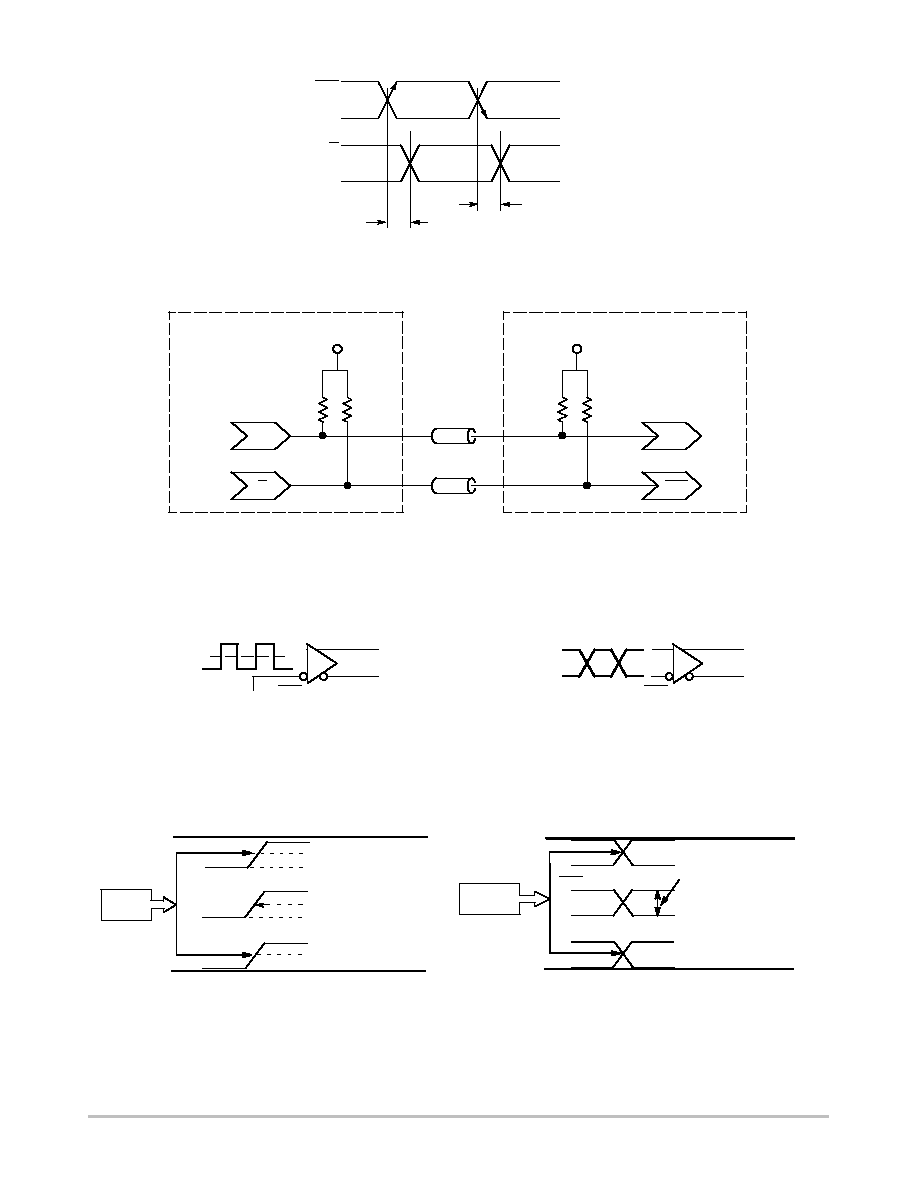
Figure 8. AC Reference Measurement
CLK
CLK
Q
Q
t
PHL
t
PLH
V
INPP
= V
IH
(CLK) - V
IL
(CLK)
V
OUTPP
= V
OH
(Q) - V
OL
(Q)
Figure 9. Typical Termination for Output Driver Using External Termination Resistor
(Refer to Application Notes AND8020/D and AND8173/D)
NB7L11M
Receiver
Device
Q
CLK
Q
CLK
V
CC
50
W
50
W
V
CC
50
W
50
W
Z = 50
W
Z = 50
W
Figure 10. Differential Input Driven
Single-Ended
Figure 11. Differential Inputs Driven
Differentially
Figure 12. V
th
Diagram
Figure 13. V
CMR
Diagram
CLK
V
CC
GND
V
IH
V
IHmin
V
IHmax
V
thmax
V
th
V
th
V
thmin
V
CMmax
V
CMmax
CLK
V
CMR
V
CC
GND
CLK
CLK
V
th
V
th
CLK
CLK
V
ILmax
V
IL
V
ILmin
CLK
V
ILCLKmax
V
IHCLKmax
V
(CLK)
= V
IHCLK
- V
ILCLK
V
ILCLKtyp
V
IHCLKtyp
V
ILCLKmin
V
IHCLKmin
NB7L11M
http://onsemi.com
8
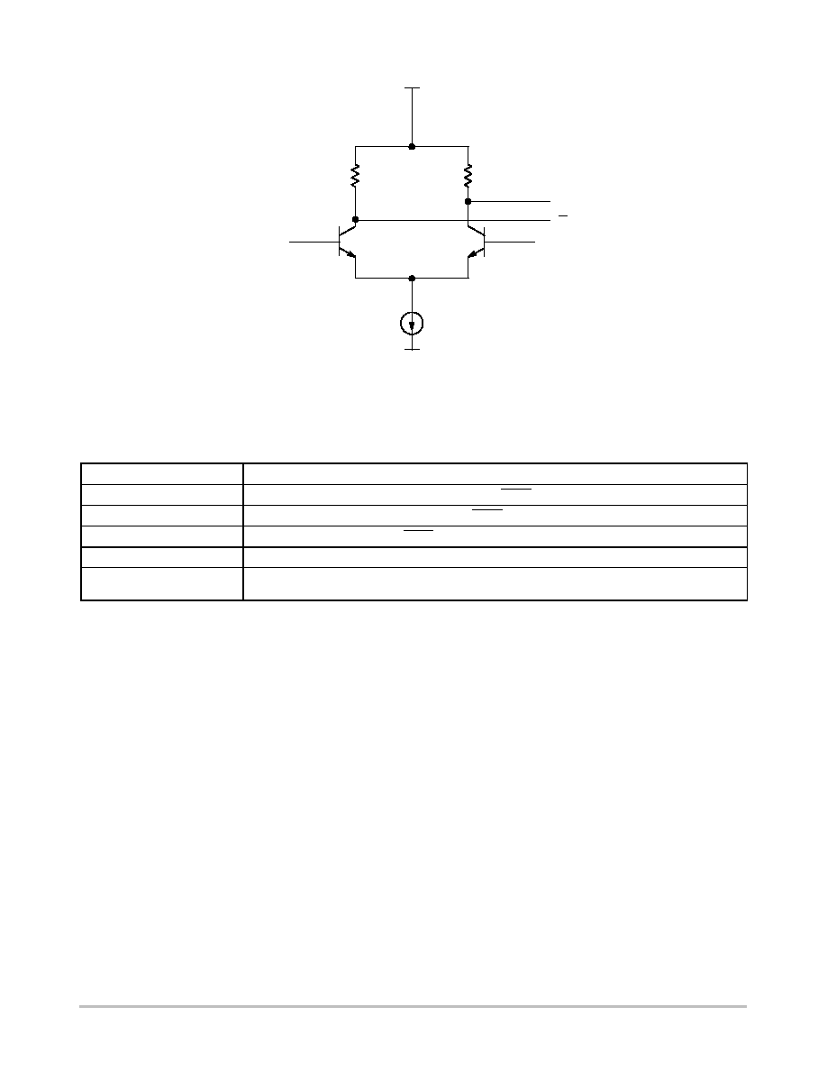
Q
Q
V
CC
16 mA
50
W
50
W
Figure 14. CML Output Structure
V
EE
Table 6. INTERFACING OPTIONS
INTERFACING OPTIONS
CONNECTIONS
CML
Connect V
TCLK
, V
TCLK
to V
CC
LVDS
Connect V
TCLK
, V
TCLK
together CLK input
AC-COUPLED
Bias V
TCLK
, V
TCLK
Inputs within (V
CMR
) Common Mode Range
RSECL, LVPECL
Standard ECL Termination Techniques. See AND8020/D.
LVTTL, LVCMOS
An external voltage should be applied to the unused complementary differential input.
Nominal voltage is 1.5 V for LVTTL and V
CC
/2 for LVCMOS inputs.
NB7L11M
http://onsemi.com
9
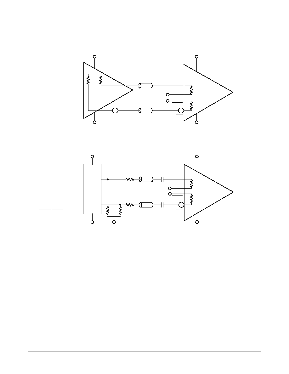
Application Information
All NB7L11M inputs can accept PECL, CML, LVTTL,
LVCMOS and LVDS signal levels. The limitations for
differential input signal (LVDS, PECL, or CML) are
minimum input swing of 75 mV and the maximum input
swing of 2500 mV. Within these conditions, the input
voltage can range from V
CC
to 1.2 V. Examples interfaces
are illustrated below in a 50
W environment (Z = 50 W).
50
W
V
CC
CLK
CLK
50
W
NB7L11M
V
CC
V
TCLK
V
EE
V
CC
Q
50
W
50
W
CML Driver
V
EE
Figure 15. CML to CML Interface
Z
Q
Z
Figure 16. PECL to CML Receiver Interface
50
W
Z
Z
V
CC
V
CC
PECL
Driver
CLK
CLK
50
W
NB7L11M
V
EE
V
Bias
V
TCLK
V
EE
R
T
R
T
V
EE
V
CC
R
T
5.0 V 290
W
3.3 V 150
W
2.5 V
80
W
Recommended R
T
Values
50
W
50
W
V
TCLK
V
CC
V
TCLK
V
Bias
NB7L11M
http://onsemi.com
10
50
W
Z
V
CC
V
CC
LVTTL/
LVCMOS
Driver
CLK
CLK
50
W
NB7L11M
V
EE
V
TCLK
V
CC
V
REF
LVCMOS V
CC
- V
EE
2
LVTTL
1.5 V
Recommended V
REF
Values
V
TCLK
V
REF
No Connect*
No Connect
50
W
Z
V
CC
V
CC
LVDS
Driver
CLK
CLK
50
W
NB7L11M
V
EE
V
TCLK
V
EE
V
TCLK
Z
Figure 17. LVDS to CML Receiver Interface
Figure 18. LVCMOS/LVTTL to CML Receiver Interface
*or 60 pF to GND

NB7L11M
http://onsemi.com
11
ORDERING INFORMATION
Device
Package
Shipping
NB7L11MMN
QFN-16
123 Units/Rail
NB7L11MMNR2
QFN-16
3000 Tape & Reel
NB7L11MMNG
QFN-16
(Pb-Free)
123 Units/Rail
NB7L11MMNR2G
QFN-16
(Pb-Free)
3000 Tape & Reel
For information on tape and reel specifications, including part orientation and tape sizes, please refer to our Tape and Reel Packaging
Specifications Brochure, BRD8011/D.

NB7L11M
http://onsemi.com
12
PACKAGE DIMENSIONS
16 PIN QFN
MN SUFFIX
CASE 485G-01
ISSUE B
16X
SEATING
PLANE
L
D
E
0.15 C
A
A1
e
D2
E2
b
1
4
5
8
12
9
16
13
«««
«««
«««
B
A
0.15 C
TOP VIEW
SIDE VIEW
BOTTOM VIEW
PIN 1
LOCATION
0.10 C
0.08 C
(A3)
C
16 X
e
16X
NOTE 5
0.10 C
0.05 C
A B
NOTE 3
K
16X
EXPOSED PAD
NOTES:
1. DIMENSIONING AND TOLERANCING PER
ASME Y14.5M, 1994.
2. CONTROLLING DIMENSION: MILLIMETERS.
3. DIMENSION b APPLIES TO PLATED
TERMINAL AND IS MEASURED BETWEEN
0.25 AND 0.30 MM FROM TERMINAL.
4. COPLANARITY APPLIES TO THE EXPOSED
PAD AS WELL AS THE TERMINALS.
5. L
max
CONDITION CAN NOT VIOLATE 0.2 MM
MINIMUM SPACING BETWEEN LEAD TIP
AND FLAG
DIM
MIN
MAX
MILLIMETERS
A
0.80
1.00
A1
0.00
0.05
A3
0.20 REF
b
0.18
0.30
D
3.00 BSC
D2
1.65
1.85
E
3.00 BSC
E2
1.65
1.85
e
0.50 BSC
K
0.20
---
L
0.30
0.50
ON Semiconductor and are registered trademarks of Semiconductor Components Industries, LLC (SCILLC). SCILLC reserves the right to make changes without further notice
to any products herein. SCILLC makes no warranty, representation or guarantee regarding the suitability of its products for any particular purpose, nor does SCILLC assume any liability
arising out of the application or use of any product or circuit, and specifically disclaims any and all liability, including without limitation special, consequential or incidental damages.
"Typical" parameters which may be provided in SCILLC data sheets and/or specifications can and do vary in different applications and actual performance may vary over time. All
operating parameters, including "Typicals" must be validated for each customer application by customer's technical experts. SCILLC does not convey any license under its patent rights
nor the rights of others. SCILLC products are not designed, intended, or authorized for use as components in systems intended for surgical implant into the body, or other applications
intended to support or sustain life, or for any other application in which the failure of the SCILLC product could create a situation where personal injury or death may occur. Should
Buyer purchase or use SCILLC products for any such unintended or unauthorized application, Buyer shall indemnify and hold SCILLC and its officers, employees, subsidiaries, affiliates,
and distributors harmless against all claims, costs, damages, and expenses, and reasonable attorney fees arising out of, directly or indirectly, any claim of personal injury or death
associated with such unintended or unauthorized use, even if such claim alleges that SCILLC was negligent regarding the design or manufacture of the part. SCILLC is an Equal
Opportunity/Affirmative Action Employer. This literature is subject to all applicable copyright laws and is not for resale in any manner.
PUBLICATION ORDERING INFORMATION
N. American Technical Support: 800-282-9855 Toll Free
USA/Canada
Japan: ON Semiconductor, Japan Customer Focus Center
2-9-1 Kamimeguro, Meguro-ku, Tokyo, Japan 153-0051
Phone: 81-3-5773-3850
NB7L11M/D
LITERATURE FULFILLMENT:
Literature Distribution Center for ON Semiconductor
P.O. Box 61312, Phoenix, Arizona 85082-1312 USA
Phone: 480-829-7710 or 800-344-3860 Toll Free USA/Canada
Fax: 480-829-7709 or 800-344-3867 Toll Free USA/Canada
Email: orderlit@onsemi.com
ON Semiconductor Website: http://onsemi.com
Order Literature: http://www.onsemi.com/litorder
For additional information, please contact your
local Sales Representative.