 | ÐлекÑÑоннÑй компоненÑ: NBSG111BA | СкаÑаÑÑ:  PDF PDF  ZIP ZIP |
NBSG111
©
Semiconductor Components Industries, LLC, 2003
May, 2003 - Rev. 7
1
Publication Order Number:
NBSG111/D
NBSG111
2.5V/3.3V SiGe Differential
1:10 Clock/Data Driver
with RSECL* Outputs
*Reduced Swing ECL
The NBSG111 is a 1-to-10 differential clock/data driver. The
device is functionally equivalent to the LVEP111 device with much
higher bandwidth and lower EMI capabilities.
Inputs incorporate internal 50
W termination resistors (input to VT
pad) and accept NECL (Negative ECL), PECL (Positive ECL),
LVTTL, LVCMOS, CML, or LVDS. Outputs are RSECL (Reduced
Swing ECL), 400 mV.
The Q[0:9] / Q[0:9] outputs have a differential synchronous enable
(EN/EN) pin. The synchronous enable pin is used to avoid a runt clock
pulse when the device is enabled/disabled as can happen with an
asynchronous control. The internal flip flop is clocked on the falling
edge of selected clock (CLK0/CLK0 or CLK1/CLK1), therefore all
associated specification limits are referenced to the negative edge of
the selected clock input.
The V
BB
and V
MM
pins are internally generated voltage supplies
available to this device only. The V
BB
is used for single-ended NECL
or PECL inputs and the V
MM
pin is used for LVCMOS inputs. For
single- ended input operation, the unused differential input is
connected to V
BB
or V
MM
as a switching reference voltage. V
BB
or
V
MM
may also rebias AC coupled inputs. When used, decouple V
BB
and V
MM
via a 0.01
mF capacitor and limit current sourcing or sinking
to 0.5 mA. When not used, V
BB
and V
MM
outputs should be left open.
·
Maximum Input Clock Frequency > 6 GHz Typical
·
Maximum Input Data Rate > 6 Gb/s Typical
·
300 ps Typical Propagation Delay
·
60 ps Typical Rise and Fall Times
·
RSPECL Output with Operating Range: V
CC
= 2.375 V to
3.465 V with V
EE
= 0 V
·
RSNECL Output with RSNECL or NECL Inputs with
Operating Range: V
CC
= 0 V with V
EE
= -2.375 V to -3.465 V
·
RSECL Output Level (400 mV Peak-to-Peak Output), Differential
Output
·
50
W Internal Input Termination Resistors
·
Compatible with Existing 2.5 V/3.3 V LVEP and EP Devices
·
V
BB
and V
MM
Reference Voltage Output
SG111 = Device Code
L
= Wafer Lot
Y
= Year
W
= Work Week
*For further details, refer to Application Note
AND8002/D
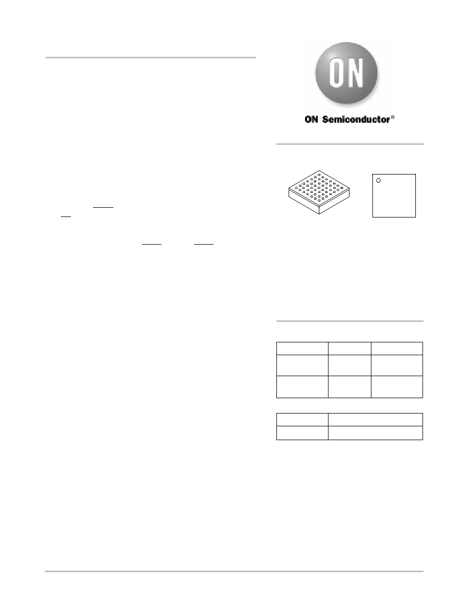
FCBGA-49
BA SUFFIX
CASE 489A
MARKING
DIAGRAM*
SG
111
Device
Package
Shipping
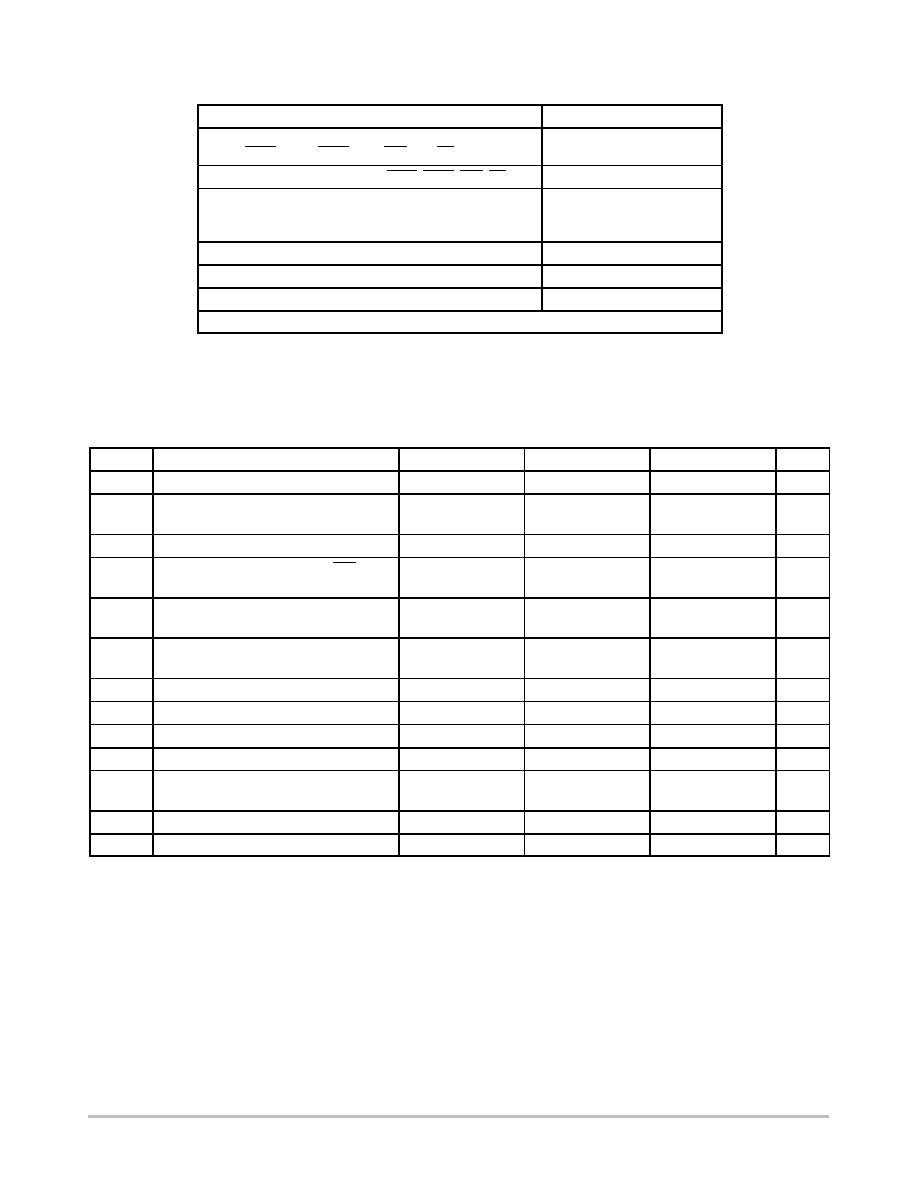
ORDERING INFORMATION
NBSG111BA
8x8 mm
FCBGA-49
100 Units/Tray
NBSG111BAR2
8x8 mm
FCBGA-49
500/Tape & Reel
LYW
Board
Description
NBSG111BAEVB
NBSG111BA Evaluation Board
http://onsemi.com
NBSG111
http://onsemi.com
2
VCC
NC
Q7
Figure 1. BGA-49 Pinout (Top View)
V
EE
Q0
Q0
V
EE
Q1
EN
V
MM
Q9
Q9
Q8
CLK1
VTCLK1
VTEN
V
CC
VTCLK1
CLK1
A
B
C
D
1
2
3
4
Q8
Q7
V
EE
5
6
7
VTSEL
SEL
Q6
VTSEL
SEL
Q6
Q1
Q2
V
EE
Q2
NC
EN
VTEN
V
CC
Q3
VTCLK0
Q3
CLK0
CLK0
VTCLK0
Q4
V
BB
V
EE
Q4
Q5
Q5
V
EE
E
F
G
NBSG111
http://onsemi.com
3
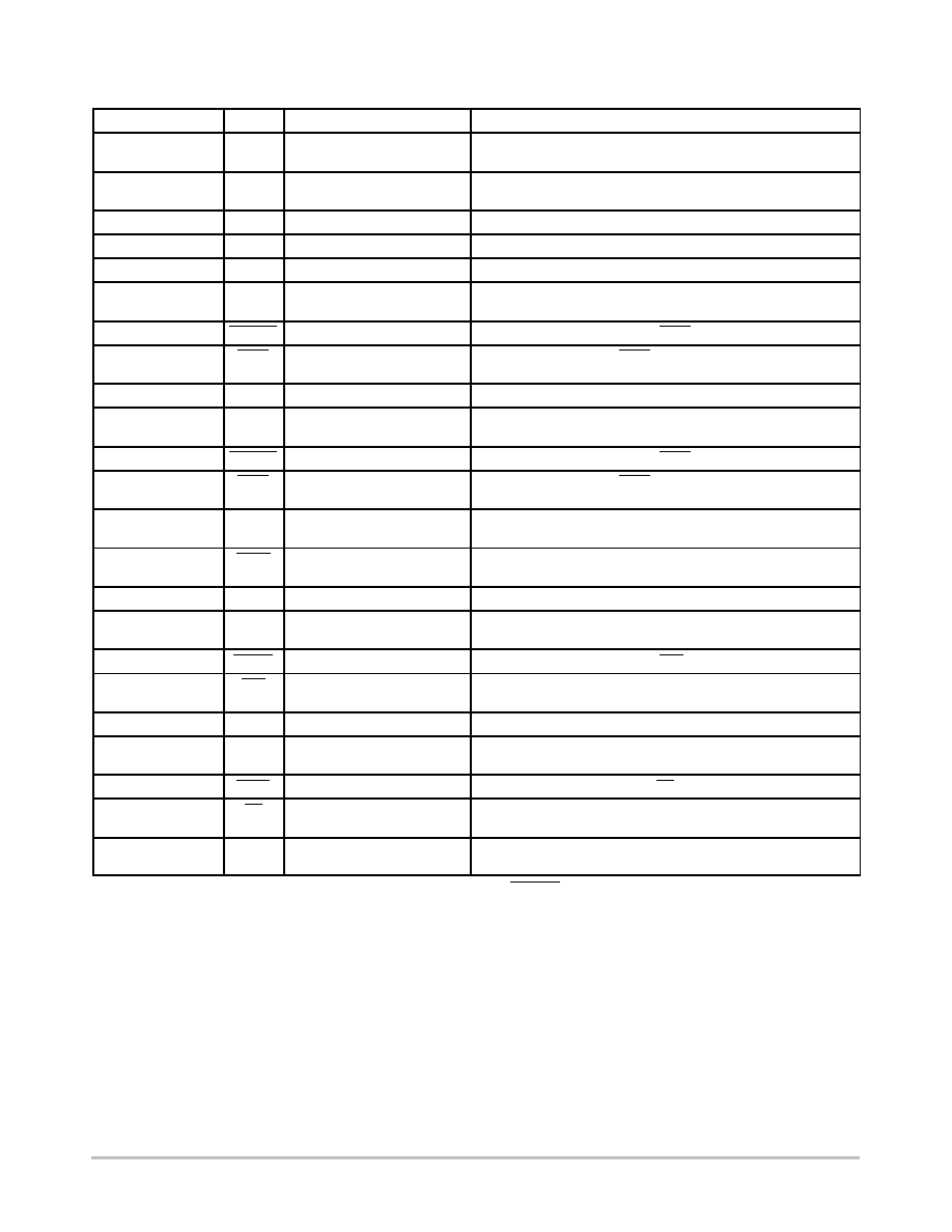
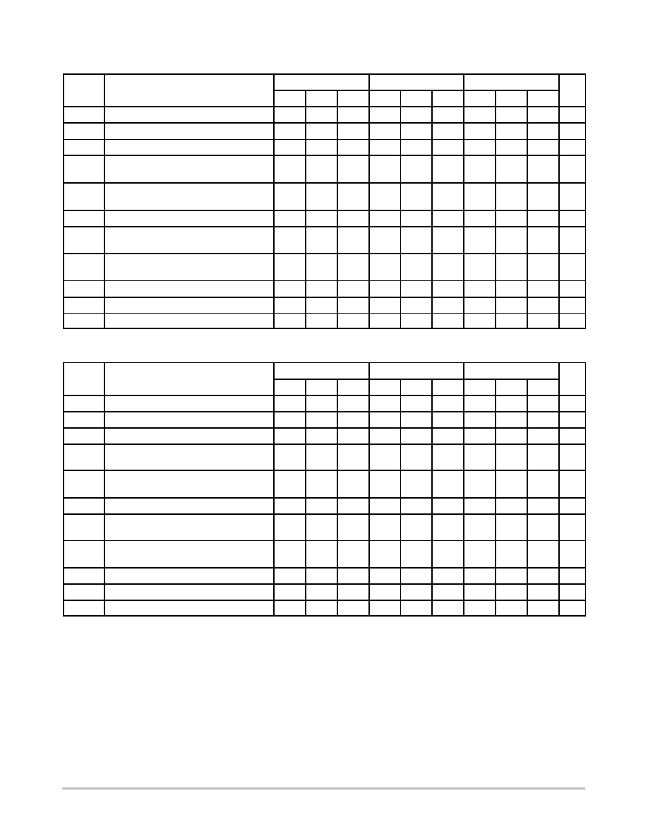
Table 1. Pin Description
Pin
Name
I/O
Description
A1,A7,G1,G7,C2,E6
V
EE
-
Negative Supply Voltage. All V
EE
Pins Must be Externally Con-
nected to Power Supply to Guarantee Proper Operation.
F3,D4,B5
V
CC
-
Positive Supply Voltage. All V
CC
Pins Must be Externally Connected
to Power Supply to Guarantee Proper Operation.
B2
V
MM
-
LVCMOS Reference Voltage Output (V
CC
- V
EE
) / 2.
F6
V
BB
-
ECL Reference Voltage Output
E4
VTCLK0
-
Internal 50
W
Termination Pin for CLK0. See Table 4. (Note 1)
F4
CLK0
ECL, CML, LVCMOS, LVDS,
LVTTL Input
Noninverted Differential Input CLK0. Internal 75 k
W
to V
EE
.
E5
VTCLK0
-
Internal 50
W
Termination Pin for CLK0. See Table 4. (Note 1)
F5
CLK0
ECL, CML, LVCMOS, LVDS,
LVTTL Input
Inverted Differential Input CLK0. Internal 75 k
W
to V
EE
and 36.5 k
W
to V
CC
.
C4
VTCLK1
-
Internal 50
W
Termination Pin 1. See Table 4. (Note 1)
B4
CLK1
ECL, CML, LVCMOS, LVDS,
LVTTL Input
Noninverted Differential Input CLK1. Internal 75 k
W
to V
EE
.
C3
VTCLK1
-
Internal 50
W
Termination Pin for CLK1. See Table 4. (Note 1)
B3
CLK1
ECL, CML, LVCMOS, LVDS,
LVTTL Input
Inverted Differential Input CLK1. Internal 75 k
W
to V
EE
and 36.5 k
W
to V
CC
.
B1,D1,F1,G3,G5,F7,
D7,B7,A5,A3
Q[0:9]
RSECL Output
Noninverted Differential Outputs [0:9]. Typically Terminated with
50
W
to V
TT
= V
CC
- 1.5 V
C1,E1,G2,G4,G6,E7,
C7,A6,A4,A2
Q[0:9]
RSECL Output
Inverted Differential Outputs [0:9]. Typically Terminated with 50
W
to
V
TT
= V
CC
- 1.5 V
D5
VTSEL
-
Internal 50
W
Termination Pin for SEL. See Table 4. (Note 1)
D6
SEL
ECL, CML, LVCMOS, LVDS,
LVTTL Input
Noninverted Differential Select Logic Input. Internal 75 k
W
to V
EE
.
C5
VTSEL
-
Internal 50
W
Termination Pin for SEL. See Table 4. (Note 1)
C6
SEL
ECL, CML, LVCMOS, LVDS,
LVTTL Input
Inverted Differential Select Logic Input. Internal 75 k
W
to V
EE
and
36.5 k
W
to V
CC
.
D3
VTEN
-
Internal 50
W
Termination Pin for EN. See Table 4. (Note 1)
D2
EN
ECL, CML, LVCMOS, LVDS,
LVTTL Input
Noninverted Differential Output Enable Pin. Internal 75 k
W
to V
EE
.
E3
VTEN
-
Internal 50
W
termination Pin for EN. See Table 4. (Note 1)
E2
EN
ECL, CML, LVCMOS, LVDS,
LVTTL Input
Inverted Differential Output Enable Pin. Internal 75 k
W
to V
EE
and
36.5 k
W
to V
CC
.
F2,B6
NC
-
No Connect. The NC Pins are Electrically Connected to the Die and
"MUST BE" Left Open.
1. In the differential configuration when the input termination pins (VTCLK, VTDCLK) are connected to a common termination voltage and
if no signal is applied, then the device will be susceptible to self-oscillation.
NBSG111
http://onsemi.com
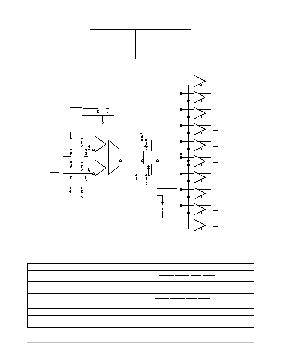
4
(F6) V
BB
0
1
(F4) CLK0
(F5) CLK0
(B4) CLK1
(B3) CLK1
(D6) SEL
Q
0
(B1)
Q
0
(C1)
Q
1
(D1)
Q
1
(E1)
Q
2
(F1)
Q
2
(G2)
Q
3
(G3)
Q
3
(G4)
Q
4
(G5)
Q
4
(G6)
Q
5
(F7)
Q
5
(E7)
Q
6
(D7)
Q
6
(C7)
Q
7
(B7)
Q
7
(A6)
Q
8
(A5)
Q
8
(A4)
Q
9
(A3)
Q
9
(A2)
(A1, A7, G1, G7) V
EE
(B5, D4, F3) V
CC
Table 2. FUNCTION TABLE
Active Input
Disabled Outputs
CLK0, CLK0
Disabled Outputs
CLK1, CLK1
SEL
L
L
H
H
EN
L
H
L
H
(B2) V
MM
(E3) VTEN
(E2) EN
(D3) VTEN
(D2) EN
(C6) SEL
(C5) VTSEL
(E4) VTCLK0
(E5) VTCLK0
(C4) VTCLK1
(C3) VTCLK1
(D5) VTSEL
Figure 2. Logic Diagram
SYNC
2. SEL/EN are the inverse of SEL/EN unless specified otherwise.
R
TIN
R
1
R
2
R
TIN
R
2
R
TIN
R
2
R
1
R
2
R
2
R
1
R
TIN
R
TIN
R
TIN
R
TIN
R
2
R
2
R
TIN
R
2
R
1
Table 3. INTERFACING OPTIONS
INTERFACING OPTIONS
CONNECTIONS
CML
Connect VTCLK0, VTCLK1, VTEN, VTSEL and
VTCLK0, VTCLK1, VTEN, VTSEL to V
CC
LVDS
Connect VTCLK0, VTCLK1, VTEN, VTSEL and
VTCLK0, VTCLK1, VTEN, VTSEL Together
AC-COUPLED
Bias VTCLK0, VTCLK1, VTEN, VTSEL and
VTCLK0, VTCLK1, VTEN, VTSEL Inputs within
Common Mode Range (V
IHCMR
)
RSECL, PECL, NECL
Standard ECL Termination Techniques
LVTTL, LVCMOS
See Text on Page 1. Unused Differential Input Switching Voltage
Reference Range is from V
EE
+ 1125 mV to V
CC
- 75 mV
NBSG111
http://onsemi.com
5
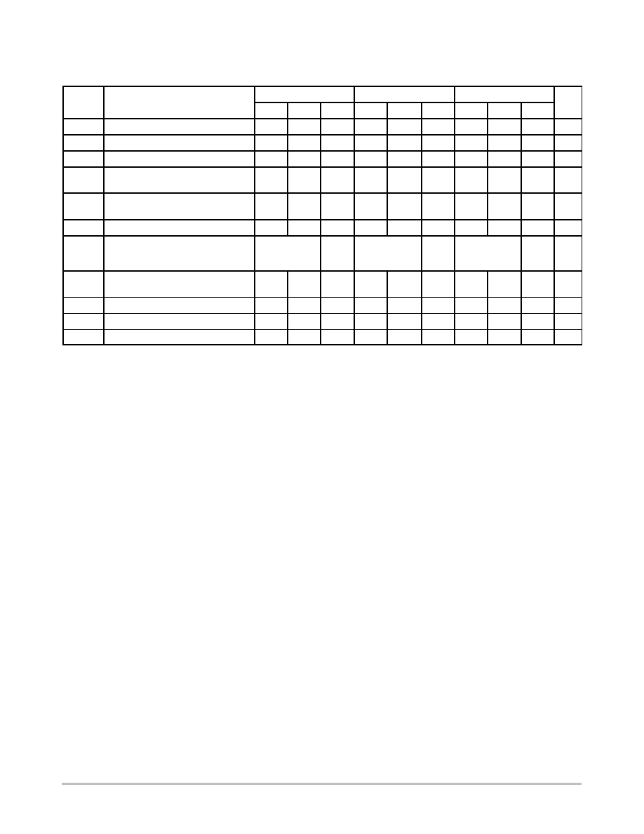
Table 4. ATTRIBUTES
Characteristics
Value
Internal Input Pulldown Resistor, R2
(CLK0, CLK0, CLK1, CLK1, SEL, SEL, EN, EN)
75 k
W
Internal Input Pullup Resistor, R1 (CLK0, CLK1, SEL, EN)
36.5 k
W
ESD Protection
Human Body Model
Machine Model
Charged Device Model
> 2 kV
> 100 V
> 1 kV
Moisture Sensitivity (Note 3)
Level 3
Flammability Rating
Oxygen Index: 28 to 34
UL 94 V-0 @ 0.125 in
Transistor Count
479
Meets or exceeds JEDEC Spec EIA/JESD78 IC Latchup Test
3. For additional information, see Application Note AND8003/D.
Table 5. MAXIMUM RATINGS
(Note 4)
Symbol
Parameter
Condition 1
Condition 2
Rating
Units
V
CC
Positive Power Supply
V
EE
= 0 V
3.6
V
V
I
Positive Input
Negative Input
V
EE
= 0 V
V
CC
= 0 V
V
I
V
CC
V
I
V
EE
3.6
-3.6
V
V
V
EE
Negative Power Supply
V
CC
= 0 V
-3.6
V
V
INPP
Differential Input Voltage |CLK - CLK|
V
CC
- V
EE
w
2.8 V
V
CC
- V
EE
t
2.8 V
2.8
|V
CC
- V
EE
|
V
V
I
OUT
Output Current
Continuous
Surge
25
50
mA
mA
I
IN
Input Current Through R
T
(50
W
Resistor)
Static
Surge
45
80
mA
mA
I
BB
V
BB
Sink/Source
1
mA
I
MM
V
MM
Sink/Source
1
mA
TA
Operating Temperature Range
-40 to +70
°
C
T
stg
Storage Temperature Range
-65 to +150
°
C
q
JA
Thermal Resistance (Junction-to-Ambient)
(Note 5)
0 LFPM
500 LFPM
49 FCBGA
49 FCBGA
67
57
°
C/W
°
C/W
q
JC
Thermal Resistance (Junction-to-Case)
2S2P (Note 5)
49 FCBGA
2 to 4
°
C/W
T
sol
Wave Solder
< 15 sec.
225
°
C
4. Maximum Ratings are those values beyond which device damage may occur.
5. JEDEC standard 51-6, multilayer board - 2S2P (2 signal, 2 power).
NBSG111
http://onsemi.com
6
Table 6. DC CHARACTERISTICS, INPUT WITH RSPECL OUTPUT
V
CC
= 2.5 V; V
EE
= 0 V (Note 6)
-40
°
C
25
°
C
70
°
C
Symbol
Characteristic
Min
Typ
Max
Min
Typ
Max
Min
Typ
Max
Unit
I
EE
Negative Power Supply Current
70
85
100
70
85
100
70
85
100
mA
V
OH
Output HIGH Voltage (Note 7)
1490
1540
1590
1510
1560
1610
1520
1570
1620
mV
V
OUTPP
Output Voltage Amplitude
300
370
450
300
370
450
300
370
450
mV
V
IH
Input HIGH Voltage
(Single-Ended) (Notes 9 and 10)
V
THR
+ 75
V
CC
-
1000*
V
CC
V
THR
+ 75
V
CC
-
1000*
V
CC
V
THR
+ 75
V
CC
-
1000*
V
CC
mV
V
IL
Input LOW Voltage
(Single-Ended) (Notes 9 and 11)
V
IH
-
2500
V
CC
-
1400*
V
THR
- 75
V
IH
-
2500
V
CC
-
1400*
V
THR
- 75
V
IH
-
2500
V
CC
-
1400*
V
THR
- 75
mV
V
BB
PECL Output Voltage Reference
1080
1140
1200
1080
1140
1200
1080
1140
1200
mV
V
IHCMR
Input HIGH Voltage Common Mode
Range (Differential Configuration) (Note 8)
1.2
2.5
1.2
2.5
1.2
2.5
V
V
MM
LVCMOS Output Voltage Reference
(V
CC
- V
EE
) / 2
1100
1250
1400
1100
1250
1400
1100
1250
1400
mV
R
TIN
Internal Input Termination Resistor
45
50
55
45
50
55
45
50
55
W
I
IH
Input HIGH Current (@ V
IH
)
30
100
30
100
30
100
m
A
I
IL
Input LOW Current (@ V
IL
)
25
100
25
100
25
100
m
A
Table 7. DC CHARACTERISTICS, INPUT WITH RSPECL OUTPUT
V
CC
= 3.3 V; V
EE
= 0 V (Note 12)
-40
°
C
25
°
C
70
°
C
Symbol
Characteristic
Min
Typ
Max
Min
Typ
Max
Min
Typ
Max
Unit
I
EE
Negative Power Supply Current
70
85
100
70
85
100
70
85
100
mA
V
OH
Output HIGH Voltage (Note 7)
2290
2340
2390
2310
2360
2410
2320
2370
2420
mV
V
OUTPP
Output Voltage Amplitude
300
370
450
300
370
450
300
370
450
mV
V
IH
Input HIGH Voltage
(Single-Ended) (Notes 9 and 10)
V
THR
+ 75
V
CC
-
1000*
V
CC
V
THR
+ 75
V
CC
-
1000*
V
CC
V
THR
+ 75
V
CC
-
1000*
V
CC
mV
V
IL
Input LOW Voltage
(Single-Ended) (Notes 9 and 11)
V
IH
-
2500
V
CC
-
1400*
V
THR
- 75
V
IH
-
2500
V
CC
-
1400*
V
THR
- 75
V
IH
-
2500
V
CC
-
1400*
V
THR
- 75
mV
V
BB
PECL Output Voltage Reference
1880
1940
2000
1880
1940
2000
1880
1940
2000
mV
V
IHCMR
Input HIGH Voltage Common Mode
Range (Differential Configuration) (Note 8)
1.2
3.3
1.2
3.3
1.2
3.3
V
V
MM
LVCMOS Output Voltage Reference
(V
CC
- V
EE
)/2
1500
1650
1800
1500
1650
1800
1500
1650
1800
mV
R
TIN
Internal Input Termination Resistor
45
50
55
45
50
55
45
50
55
W
I
IH
Input HIGH Current (@ V
IH
)
30
100
30
100
30
100
m
A
I
IL
Input LOW Current (@ V
IL
)
25
100
25
100
25
100
m
A
NOTE: SiGe circuits are designed to meet the DC specifications shown in the above tables after thermal equilibrium has been established. The
circuit is in a test socket or mounted on a printed circuit board and transverse airflow greater than 500 lfpm is maintained.
6. Input and output parameters vary 1:1 with V
CC
. V
EE
can vary +0.125 V to -0.965 V.
7. All outputs loaded with 50
W
to V
CC
- 1.5 V. V
OH
/V
OL
measured at V
IH
/V
IL
(Typical).
8. V
IHCMR
min varies 1:1 with V
EE
, V
IHCMR
max varies 1:1 with V
CC
. The V
IHCMR
range is referenced to the most positive side of the differential
input signal.
9. V
THR
is the voltage applied to the complementary input, typically V
BB
or V
MM
. V
THR(MIN)
= V
IHCMR
+ 75 mV. V
THR(MAX)
= V
IHCMR
- 75 mV.
10. V
IH
cannot exceed V
CC
.
11. V
IL
always
w
V
EE
.
12. Input and output parameters vary 1:1 with V
CC
. V
EE
can vary +0.925 V to -0.165 V.
*Typicals used for testing purposes.
NBSG111
http://onsemi.com
7
Table 8. DC CHARACTERISTICS, NECL OR RSNECL INPUT WITH NECL OUTPUT
V
CC
= 0 V; V
EE
= -3.465 V to -2.375 V (Note 13)
-40
°
C
25
°
C
70
°
C
Symbol
Characteristic
Min
Typ
Max
Min
Typ
Max
Min
Typ
Max
Unit
I
EE
Negative Power Supply Current
70
85
100
70
85
100
70
85
100
mA
VOH
Output HIGH Voltage (Note 14)
-1010
-960
-910
-990
-940
-890
-980
-930
-880
mV
V
OUTPP
Output Voltage Amplitude
300
370
450
300
370
450
300
370
450
mV
V
IH
Input HIGH Voltage
(Single-Ended) (Notes 16 and 17)
V
THR
+ 75
V
CC
-
1000*
V
CC
V
THR
+ 75
V
CC
-
1000*
V
CC
V
THR
+ 75
V
CC
-
1000*
V
CC
mV
V
IL
Input LOW Voltage
(Single-Ended) (Notes 16 and 18)
V
IH
-
2500
V
CC
-
1400*
V
THR
- 75
V
IH
-
2500
V
CC
-
1400*
V
THR
- 75
V
IH
-
2500
V
CC
-
1400*
V
THR
- 75
mV
V
BB
NECL Output Voltage Reference
-1420
-1360
-1300
-1420
-1360
-1300
-1420
-1360
-1300
mV
V
IHCMR
Input HIGH Voltage Common Mode
Range (Differential Configuration)
(Note 15)
V
EE
+1.2
0.0
V
EE
+1.2
0.0
V
EE
+1.2
0.0
V
V
MM
LVCMOS Output Voltage Reference
(V
CC
- V
EE
)/2 (Note 19)
V
MMT
- 150
V
MMT
V
MMT
+ 150
V
MMT
- 150
V
MMT
V
MMT
+ 150
V
MMT
- 150
V
MMT
V
MMT
+ 150
mV
R
TIN
Internal Input Termination Resistor
45
50
55
45
50
55
45
50
55
W
I
IH
Input HIGH Current (@ V
IH
)
30
100
30
100
30
100
m
A
I
IL
Input LOW Current (@ V
IL
)
25
100
25
100
25
100
m
A
NOTE: SiGe circuits are designed to meet the DC specifications shown in the above table after thermal equilibrium has been established. The
circuit is in a test socket or mounted on a printed circuit board and transverse airflow greater than 500 lfpm is maintained.
13. Input and output parameters vary 1:1 with V
CC
.
14. All outputs loaded with 50
W
to V
CC
- 1.5 V. V
OH
/V
OL
measured at V
IH
/V
IL
(Typical).
15. V
IHCMR
min varies 1:1 with V
EE
, V
IHCMR
max varies 1:1 with V
CC
. The V
IHCMR
range is referenced to the most positive side of the differential
input signal.
16. V
THR
is the voltage applied to the complementary input, typically V
BB
or V
MM
. V
THR(MIN)
= V
IHCMR
+ 75 mV. V
THR(MAX)
= V
IHCMR
- 75 mV.
17. V
IH
cannot exceed V
CC
.
18. V
IL
always
w
V
EE
.
19. V
MM
Typical = |V
CC
- V
EE
| / 2 + V
EE
= V
MMT
.
*Typicals used for testing purposes.
NBSG111
http://onsemi.com
8
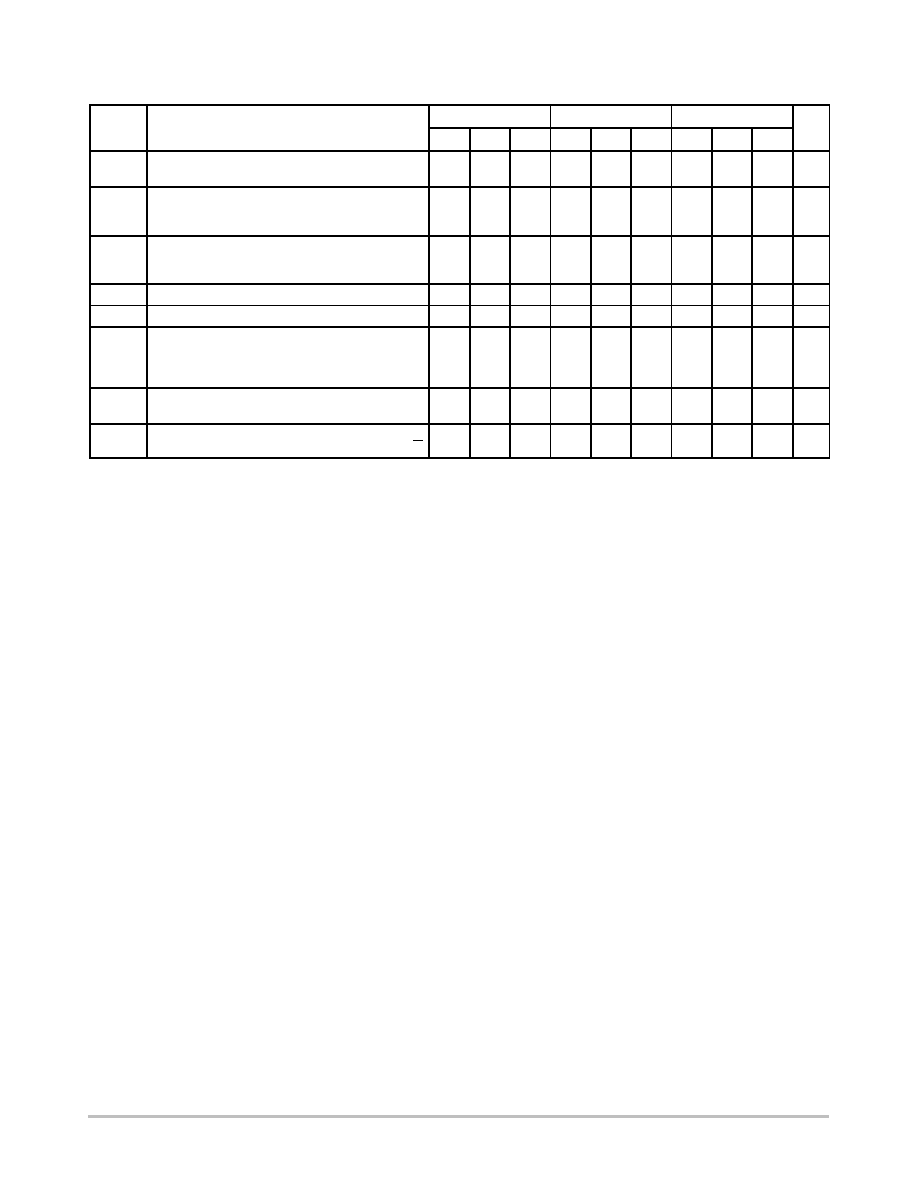
Table 9. AC CHARACTERISTICS
V
CC
= 0 V; V
EE
= -3.465 V to -2.375 V or V
CC
= 2.375 V to 3.465 V; V
EE =
0 V
-40
°
C
25
°
C
70
°
C
Symbol
Characteristic
Min
Typ
Max
Min
Typ
Max
Min
Typ
Max
Unit
V
OUTPP
Output Voltage Amplitude
f
in
< 3 GHz
(See Figure 3) (Note 20)
f
in
= 5.5 GHz
320
180
420
250
300
150
400
220
300
100
400
200
mV
t
PLH
,
t
PHL
Propagation Delay to Output Differential
Output Enable
Clock Select
250
430
400
300
550
450
350
700
500
250
430
400
300
550
450
350
700
500
250
430
400
300
600
480
350
750
550
ps
t
SKEW
Duty Cycle Skew (Note 21)
Within-Device Skew (Note 22)
Device-to-Device Skew (Note 23)
2
5
15
15
20
85
2
5
15
15
20
85
2
5
15
15
20
85
ps
t
S
Setup Time to CLK (EN to Selected CLK0:1)
110
70
110
70
115
80
ps
t
H
Hold Time (EN to Selected CLK0:1)
110
70
110
70
115
80
ps
t
JITTER
RMS Random Clock Jitter(Figure 3)
(Note 25)
f
in
= 5 GHz
Peak-to-Peak Data Dependent Jitter
(Note 26)
f
in
= 5 Gb/s
0.5
2.0
0.5
14
2.0
0.5
2.0
ps
V
INPP
Input Voltage Swing/Sensitivity
(Differential Configuration) (Note 24)
75
2600
75
2600
75
2600
mV
t
r
t
f
Output Rise/Fall Times (20% - 80%) @ 1 GHz
Q, Q
40
60
80
40
60
80
40
60
80
ps
20. Measured using a 500 mV source, 50% duty cycle clock source. All outputs loaded with 50
W
to V
CC
- 1.5 V. Input edge rates 40 ps
(20% - 80%).
21. t
SKEW
= |t
PLH
- t
PHL
| for a nominal 50% differential clock input waveform (Figure 4).
22. Within-Device skew is measured between outputs under identical transitions and conditions on any one device.
23. Device-to-Device skew for identical transitions at identical V
CC
levels.
24. V
INPP
(MAX) cannot exceed V
CC
- V
EE
(applicable only when V
CC
-V
EE
t
2600 mV).
25. Additive RMS jitter with 50% duty cycle clock signal at 5 GHz.
26. Additive Peak-to-Peak jitter with input NRZ data at PRBS 2
31
-1 at 5 Gb/s.
NBSG111
http://onsemi.com
9
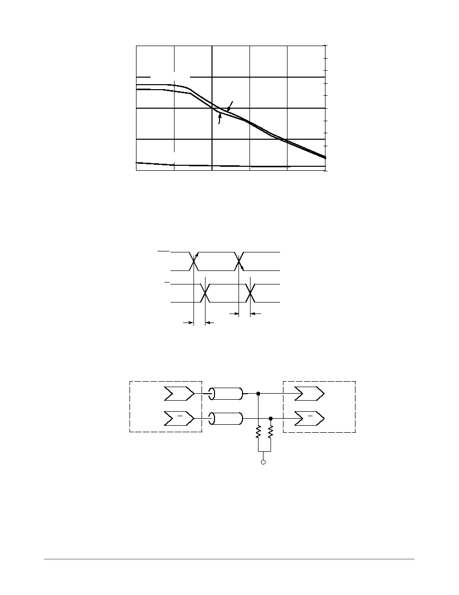
150
250
350
450
550
1
2
3
4
5
6
0.0
1.0
2.0
3.0
4.0
5.0
6.0
7.0
8.0
9.0
10.0
RMS JITTER (ps)
INPUT FREQUENCY (GHz)
Figure 3. Output Voltage Amplitude (V
OUTPP
) / RMS Jitter vs.
Input Frequency (f
in
) at Ambient Temperature (Typical)
OUTPUT VOL
T
AGE AMPLITUDE
(mV)
RMS JITTER (ps)
Q AMP (mV)
3.3 V
2.5 V
W
Driver
Device
Receiver
Device
Q
D
50
W
50
V TT
Q
D
Figure 4. AC Reference Measurement
CLK
CLK
Q
Q
t
PHL
t
PLH
V
INPP
= V
IH
(CLK) - V
IL
(CLK)
Figure 5. Typical Termination for Output Driver and Device Evaluation
(Refer to Application Note AND8020 - Termination of ECL Logic Devices)
V
TT
= V
CC
- 1.5 V
V
OUTPP
= V
OH
(Q) - V
OL
(Q)
Z = 50
W
Z = 50
W
NBSG111
http://onsemi.com
10
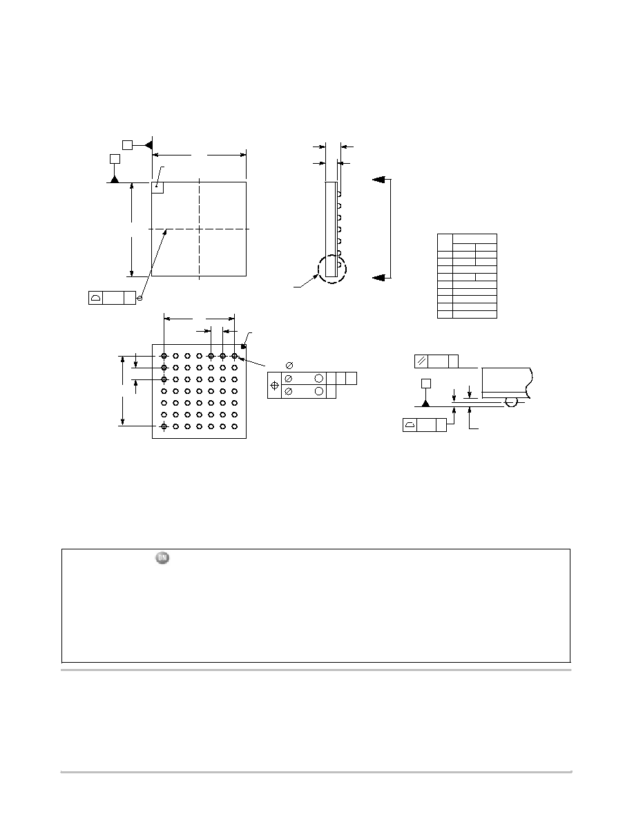
PACKAGE DIMENSIONS
FCBGA-49
BA SUFFIX
PLASTIC 8x8 mm (1.0 mm pitch) BGA FLIP CHIP PACKAGE
CASE 489A-02
ISSUE A
ÉÉ
ÉÉ
0.15
TERMINAL A1 CORNER
Z
0.12 C
0.20 C
VIEW Z-Z
E1
Z
A
0.15
C
0.08
C
b
49 X
FEDUCIAL FOR PIN A1
IDENTIFICATION IN THIS AREA
4
3
2
1
A
E
F
G
49 X
NOTES:
1. CONTROLLING DIMENSION: MILLIMETER.
2. DIMENSIONS AND TOLERANCES PER ASME
Y14.5M-1994.
3. DIMENSION b IS MEASURED AT THE MAXIMUM
SOLDER BALL DIAMETER, PARALLEL TO DATUM
PLANE C.
4. DATUM C (SEATING PLANE) IS DEFINED BY THE
SPHERICAL CROWNS OF THE SOLDER BALLS.
5. PARALLELISM MEASUREMENT SHALL EXCLUDE
ANY EFFECT OF MARK ON TOP SURFACE OF
PACKAGE.
6. 489A-01 OBSOLETE, NEW STANDARD 489A-02.
M
M
7
6
5
B
C
D
e
NOTE 5
NOTE 4
A2
A
DIM
A
MIN
MAX
MILLIMETERS
A1
A2
0.91 REF
b
0.40
0.60
D
8.00 BSC
D1
6.00 BSC
E
8.00 BSC
E1
1.00 BSC
e
A
B
E
D
C
4 X
C
D1
e
B
NOTE 3
DETAIL A
A1
SEATING
PLANE
DETAIL A
(ROTATED 90 C.W.)
_
---
1.40
6.00 BSC
0.3
0.5
ON Semiconductor and are registered trademarks of Semiconductor Components Industries, LLC (SCILLC). SCILLC reserves the right to make
changes without further notice to any products herein. SCILLC makes no warranty, representation or guarantee regarding the suitability of its products for any
particular purpose, nor does SCILLC assume any liability arising out of the application or use of any product or circuit, and specifically disclaims any and all
liability, including without limitation special, consequential or incidental damages. "Typical" parameters which may be provided in SCILLC data sheets and/or
specifications can and do vary in different applications and actual performance may vary over time. All operating parameters, including "Typicals" must be
validated for each customer application by customer's technical experts. SCILLC does not convey any license under its patent rights nor the rights of others.
SCILLC products are not designed, intended, or authorized for use as components in systems intended for surgical implant into the body, or other applications
intended to support or sustain life, or for any other application in which the failure of the SCILLC product could create a situation where personal injury or death
may occur. Should Buyer purchase or use SCILLC products for any such unintended or unauthorized application, Buyer shall indemnify and hold SCILLC
and its officers, employees, subsidiaries, affiliates, and distributors harmless against all claims, costs, damages, and expenses, and reasonable attorney fees
arising out of, directly or indirectly, any claim of personal injury or death associated with such unintended or unauthorized use, even if such claim alleges that
SCILLC was negligent regarding the design or manufacture of the part. SCILLC is an Equal Opportunity/Affirmative Action Employer.
PUBLICATION ORDERING INFORMATION
JAPAN: ON Semiconductor, Japan Customer Focus Center
2-9-1 Kamimeguro, Meguro-ku, Tokyo, Japan 153-0051
Phone: 81-3-5773-3850
ON Semiconductor Website: http://onsemi.com
For additional information, please contact your local
Sales Representative.
NBSG111/D
Literature Fulfillment:
Literature Distribution Center for ON Semiconductor
P.O. Box 5163, Denver, Colorado 80217 USA
Phone: 303-675-2175 or 800-344-3860 Toll Free USA/Canada
Fax: 303-675-2176 or 800-344-3867 Toll Free USA/Canada
Email: ONlit@hibbertco.com
N. American Technical Support: 800-282-9855 Toll Free USA/Canada