©
Semiconductor Components Industries, LLC, 2003
April, 2003 - Rev. 5
1
Publication Order Number:
NBSG16VS/D
NBSG16VS
2.5V/3.3V SiGe Differential
Receiver/Driver with
Variable Output Swing
The NBSG16VS is a differential receiver/driver targeted for high
frequency applications that require variable output swing. The device
is functionally equivalent to the EP16VS device with much higher
bandwidth and lower EMI capabilities. This device may be used for
applications driving VCSEL lasers.
Inputs incorporate internal 50
W termination resistors and accept
NECL (Negative ECL), PECL (Positive ECL), LVTTL, LVCMOS,
CML, or LVDS. The output amplitude is varied by applying a voltage
to the V
CTRL
input pin. Outputs are variable swing ECL from 100 mV
to 750 mV amplitude, optimized for operation from V
CC
- V
EE
= 3.0
V to 3.465 V.
The V
BB
and V
MM
pins are internally generated voltage supplies
available to this device only. The V
BB
is used as a reference voltage
for single-ended NECL or PECL inputs and the V
MM
pin is used as a
reference voltage for LVCMOS inputs. For single-ended input
operation, the unused complementary differential input is connected to
V
BB
or V
MM
as a switching reference voltage. V
BB
or V
MM
may also
rebias AC coupled inputs. When used, decouple V
BB
and V
MM
via a
0.01
mF capacitor and limit current sourcing or sinking to 0.5 mA.
When not used, V
BB
and V
MM
outputs should be left open.
∑
Maximum Input Clock Frequency up to 12 GHz Typical
∑
Maximum Input Data Rate up to 12 Gb/s Typical
∑
40 ps Typical Rise and Fall Times (V
CTRL
= V
CC
- 1 V)
∑
120 ps Typical Propagation Delay (V
CTRL
= V
CC
- 1 V)
∑
Variable Swing PECL Output with Operating Range: V
CC
= 2.375 V
to 3.465 V with V
EE
= 0 V
∑
Variable Swing NECL Output with NECL Inputs with
Operating Range: V
CC
= 0 V with V
EE
= -2.375 V to -3.465 V
∑
Output Level (100 mV to 750 mV Peak-to-Peak Output;
V
CC
- V
EE
= 3.0 V to 3.465 V), Differential Output Only
∑
50
W Internal Input Termination Resistors
∑
Compatible with Existing 2.5 V/3.3 V EP Devices
∑
V
BB
and V
MM
Reference Voltage Output
*For additional information, refer to Application Note
AND8002/D
FCBGA-16
BA SUFFIX
CASE 489
MARKING
DIAGRAM*
SGS
16
Device
Package
Shipping
ORDERING INFORMATION
NBSG16VSBA
4x4 mm
FCBGA-16
100 Units/Tray
NBSG16VSBAR2
4x4 mm
FCBGA-16
500/Tape & Reel
LYW
Board
Description
NBSG16VSBAEVB
NBSG16VSBA
Evaluation Board
http://onsemi.com
A = Assembly Location
L = Wafer Lot
Y = Year
W = Work Week
SG16VS
ALYW
QFN-16
MN SUFFIX
CASE 485G
NBSG16VSMN
3x3 mm
QFN-16
123 Units/Rail
NBSG16VSMNR2
3x3 mm
QFN-16
3000/Tape & Reel

NBSG16VS
http://onsemi.com
2
Figure 1. BGA-16 Pinout (Top View)
V
EE
D
D
VTD
V
EE
V
BB
VTD
NC
V
CTRL
V
EE
V
CC
V
CC
V
MM
V
EE
Q
Q
A
B
C
D
1
2
3
4
V
EE
NC V
CTRL
V
EE
V
EE
V
BB
V
MM
V
EE
V
CC
Q
Q
V
CC
VTD
D
D
VTD
5
6
7
8
16
15
14
13
12
11
10
9
1
2
3
4
NBSG16VS
Exposed Pad (EP)
Figure 2. QFN-16 Pinout (Top View)
Table 1. Pin Description
Pin
BGA
QFN
Name
I/O
Description
C2
1
VTD
-
Internal 50
W
Termination Pin. See Table 2.
C1
2
D
ECL, CML,
LVCMOS,
LVDS,
LVTTL
Input
Inverted Differential Input. Internal 75 k
W
to V
EE
and 36.5 k
W
to V
CC
.
B1
3
D
ECL, CML,
LVCMOS,
LVDS,
LVTTL
Input
Noninverted Differential Input. Internal 75 k
W
to V
EE
.
B2
4
VTD
-
Internal 50
W
Termination Pin. See Table 2.
A1,D1,A4,
D4
5,8,13,16
V
EE
-
Negative Supply Voltage
A2
6
NC
-
No Connect
A3
7
V
CTRL
Output Amplitude Swing Control. Bypass Pin to V
CC
through 0.1
m
F Capacitor.
B3,C3
9,12
V
CC
-
Positive Supply Voltage
B4
10
Q
RSECL
Output
Noninverted Differential Output. Typically Terminated with 50
W
to
V
TT
= V
CC
- 2 V
C4
11
Q
RSECL
Output
Inverted Differential Output. Typically Terminated with 50
W
to V
TT
= V
CC
- 2 V
D3
14
V
MM
-
LVCMOS Reference Voltage Output. (V
CC
- V
EE
)/2
D2
15
V
BB
-
ECL Reference Voltage Output
N/A
-
EP
-
Exposed Pad. (Note 2)
1. The NC pin is electrically connected to the die and must be left open.
2. All V
CC
and V
EE
pins must be externally connected to Power Supply to guarantee proper operation. The thermally exposed pad on package
bottom (see case drawing) must be attached to a heat-sinking conduit.
3. In the differential configuration when the input termination pins (VTD, VTD) are connected to a common termination voltage, and if no signal
is applied then the device will be susceptible to self-oscillation.

NBSG16VS
http://onsemi.com
3
50
W
50
W
VTD
D
D
VTD
V
MM
Q
Q
V
BB
V
EE
V
CC
Figure 3. Logic Diagram/
Voltage Source Implementation
75
K
W
75
K
W
36.5
K
W
V
CTRL
Q OUT
50
W
50
W
V
CC
- 2 V
V
CTRL
+
V
CC
Q OUT
Figure 4. Alternative Voltage Source Implementation
50
W
50
W
VTD
D
D
VTD
V
MM
Q
Q
V
BB
V
EE
V
CC
75
K
W
75
K
W
36.5
K
W
V
CTRL
140
W
140
W
+3.3 V
0.1
m
F
Q OUT
Q OUT
R
VAR
Table 2. INTERFACING OPTIONS
INTERFACING OPTIONS
CONNECTIONS
CML
Connect VTD and VTD to V
CC
LVDS
Connect VTD and VTD Together
AC-COUPLED
Bias VTD and VTD Inputs within
Common Mode Range (V
IHCMR
)
RSECL, PECL, NECL
Standard ECL Termination Techniques
LVTTL
An external voltage should be applied to the unused
complementary differential input. Nominal voltage is
1.5 V for LVTTL.
LVCMOS
V
MM
should be connected to the unused
complementary differential input.
NBSG16VS
http://onsemi.com
4
Table 3. ATTRIBUTES
Characteristics
Value
Internal Input Pulldown Resistor (D, D)
75 k
W
Internal Input Pullup Resistor (D)
36.5 k
W
ESD Protection
Human Body Model
Machine Model
> 2 kV
> 100 V
Moisture Sensitivity (Note 1)
FCBGA-16
QFN-16
Level 3
Level 1
Flammability Rating
Oxygen Index: 28 to 34
UL 94 V-0 @ 0.125 in
Transistor Count
192
Meets or exceeds JEDEC Spec EIA/JESD78 IC Latchup Test
1. For additional information, see Application Note AND8003/D.
Table 4. MAXIMUM RATINGS
(Note 2)
Symbol
Parameter
Condition 1
Condition 2
Rating
Units
V
CC
Positive Power Supply
V
EE
= 0 V
3.6
V
V
EE
Negative Power Supply
V
CC
= 0 V
-3.6
V
V
I
Positive Input
Negative Input
V
EE
= 0 V
V
CC
= 0 V
V
I
v
V
CC
V
I
w
V
EE
3.6
-3.6
V
V
V
INPP
Differential Input Voltage
|D - D|
V
CC
- V
EE
w
2.8 V
V
CC
- V
EE
t
2.8 V
2.8
|V
CC
- V
EE
|
V
V
I
OUT
Output Current
Continuous
Surge
25
50
mA
mA
I
IN
Input Current Through R
T
(50
W
Resistor)
Static
Surge
45
80
mA
mA
I
BB
V
BB
Sink/Source
1
mA
I
MM
V
MM
Sink/Source
1
mA
TA
Operating Temperature Range
-40 to +85
∞
C
T
stg
Storage Temperature Range
-65 to +150
∞
C
q
JA
Thermal Resistance (Junction-to-Ambient)
(Note 3)
0 LFPM
500 LFPM
0 LFPM
500 LFPM
16 FCBGA
16 FCBGA
16 QFN
16 QFN
108
86
41.6
35.2
∞
C/W
∞
C/W
∞
C/W
∞
C/W
q
JC
Thermal Resistance (Junction-to-Case)
2S2P (Note 3)
2S2P (Note 4)
16 FCBGA
16 QFN
5.0
4.0
∞
C/W
∞
C/W
T
sol
Wave Solder
< 15 sec.
225
∞
C
2. Maximum Ratings are those values beyond which device damage may occur.
3. JEDEC standard 51-6 multilayer board - 2S2P (2 signal, 2 power).
4. JEDEC standards multilayer board - 2S2P (2 signal, 2 power) with 8 filled thermal vias under exposed pad.

NBSG16VS
http://onsemi.com
5
Table 5. DC CHARACTERISTICS, INPUT WITH VARIABLE PECL OUTPUT
V
CC
= 2.5 V; V
EE
= 0 V (Note 5)
-40
∞
C
25
∞
C
85
∞
C
Symbol
Characteristic
Min
Typ
Max
Min
Typ
Max
Min
Typ
Max
Unit
I
EE
Negative Power Supply Current
18
25
32
18
25
32
18
25
32
mA
V
OH
Output HIGH Voltage (Note 6)
1315
1440
1565
1305
1430
1555
1305
1430
1555
mV
V
OL
Output LOW Voltage (Note 6)
(Max Swing)
(V
CTRL
= V
CC
- 600 mV)
645
1090
765
1210
885
1330
605
1035
725
1155
845
1275
600
1010
720
1130
840
1250
mV
V
IH
Input HIGH Voltage
(Single-Ended) (Notes 8 and 9)
V
THR
+ 75
V
CC
-
1000*
V
CC
V
THR
+ 75
V
CC
-
1000*
V
CC
V
THR
+ 75
V
CC
-
1000*
V
CC
mV
V
IL
Input LOW Voltage
(Single-Ended) (Notes 8 and 10)
V
IH
-
2500
V
CC
-
1400*
V
THR
- 75
V
IH
-
2500
V
CC
-
1400*
V
THR
- 75
V
IH
-
2500
V
CC
-
1400*
V
THR
- 75
mV
V
BB
PECL Output Voltage Reference
1080
1140
1200
1080
1140
1200
1080
1140
1200
mV
V
IHCMR
Input HIGH Voltage Common Mode
Range (Note 7)
(Differential Configuration)
1.2
2.5
1.2
2.5
1.2
2.5
V
V
MM
CMOS Output Voltage Reference
(V
CC
- V
EE
)/2
1100
1250
1400
1100
1250
1400
1100
1250
1400
mV
R
TIN
Internal Input Termination Resistor
45
50
55
45
50
55
45
50
55
W
I
IH
Input HIGH Current (@ V
IH
)
30
100
30
100
30
100
m
A
I
IL
Input LOW Current (@ V
IL
)
25
50
25
50
25
50
m
A
Table 6. DC CHARACTERISTICS, INPUT WITH VARIABLE PECL OUTPUT
V
CC
= 3.3 V; V
EE
= 0 V (Note 11)
-40
∞
C
25
∞
C
85
∞
C
Symbol
Characteristic
Min
Typ
Max
Min
Typ
Max
Min
Typ
Max
Unit
I
EE
Negative Power Supply Current
20
27
34
20
27
34
20
27
34
mA
V
OH
Output HIGH Voltage (Note 6)
2095
2220
2345
2085
2210
2335
2075
2200
2325
mV
V
OL
Output LOW Voltage (Note 6)
(Max Swing)
(V
CTRL
= V
CC
- 600 mV)
1275
1750
1395
1870
1515
1990
1285
1730
1405
1850
1525
1970
1295
1715
1415
1835
1535
1955
mV
V
IH
Input HIGH Voltage
(Single-Ended) (Notes 8 and 9)
V
THR
+ 75
V
CC
-
1000*
V
CC
V
THR
+ 75
V
CC
-
1000*
V
CC
V
THR
+ 75
V
CC
-
1000*
V
CC
mV
V
IL
Input LOW Voltage
(Single-Ended) (Notes 8 and 10)
V
IH
-
2500
V
CC
-
1400*
V
THR
- 75
V
IH
-
2500
V
CC
-
1400*
V
THR
- 75
V
IH
-
2500
V
CC
-
1400*
V
THR
- 75
mV
V
BB
PECL Output Voltage Reference
1880
1940
2000
1880
1940
2000
1880
1940
2000
mV
V
IHCMR
Input HIGH Voltage Common Mode
Range (Note 7)
(Differential Configuration)
1.2
3.3
1.2
3.3
1.2
3.3
V
V
MM
CMOS Output Voltage Reference
(V
CC
- V
EE
)/2
1500
1650
1800
1500
1650
1800
1500
1650
1800
mV
R
TIN
Internal Input Termination Resistor
45
50
55
45
50
55
45
50
55
W
I
IH
Input HIGH Current (@ V
IH
)
30
100
30
100
30
100
m
A
I
IL
Input LOW Current (@ V
IL
)
25
50
25
50
25
50
m
A
NOTE: SiGe circuits are designed to meet the DC specifications shown in the above tables after thermal equilibrium has been established. The
circuit is in a test socket or mounted on a printed circuit board and transverse airflow greater than 500 lfpm is maintained.
5. Input and output parameters vary 1:1 with V
CC
. V
EE
can vary +0.125 V to -0.965 V.
6. All loading with 50
W
to V
CC
-2.0 volts. V
OH
/V
OL
measured at V
IH
/V
IL
.
7. V
IHCMR
min varies 1:1 with V
EE
, V
IHCMR
max varies 1:1 with V
CC
. The V
IHCMR
range is referenced to the most positive side of the differential
input signal.
8. V
THR
is the voltage applied to the complementary input, typically V
BB
or V
MM
. V
THR(MIN)
= V
IHCMR
+ 75 mV. V
THR(MAX)
= V
IHCMR
- 75 mV.
9. V
IH
cannot exceed V
CC
.
10. V
IL
always
w
V
EE
.
11. Input and output parameters vary 1:1 with V
CC
. V
EE
can vary +0.925 V to -0.165 V.
*Typicals used for testing purposes.

NBSG16VS
http://onsemi.com
6
Table 7. DC CHARACTERISTICS, NECL INPUT WITH VARIABLE NECL OUTPUT
V
CC
= 0 V; V
EE
= -3.465 V to -2.375 V (Note 12)
-40
∞
C
25
∞
C
85
∞
C
Symbol
Characteristic
Min
Typ
Max
Min
Typ
Max
Min
Typ
Max
Unit
I
EE
Negative Power Supply Current
20
27
34
20
27
34
20
27
34
mA
VOH
Output HIGH Voltage (Note 13)
-3.465 V
v
V
EE
v
-3.0 V
-3.0 V
t
V
EE
v
-2.375 V
-1205
-1 185
-1080
-1060
-955
-935
-1215
-1 195
-1090
-1070
-965
-945
-1225
-1 195
-1 100
-1070
-975
-945
mV
V
OL
Output LOW Voltage (Note 13)
-3.465 V
v
V
EE
v
-3.0 V
(Max Swing)
(V
CTRL
= V
CC
- 600 mV)
-3.0 V
t
V
EE
v
-2.375 V
(Max Swing)
(V
CTRL
= V
CC
- 600 mV)
-2000
-1560
-1855
-1410
-1910
-1440
-1620
-1215
-1820
-1320
-1290
-1000
-1990
-1580
-1895
-1460
-1900
-1460
-1705
-1290
-1810
-1340
-1425
-1 100
-1980
-1595
-1900
-1490
-1890
-1475
-1730
-1330
-1800
-1355
-1470
-1 150
mV
mV
V
IH
Input HIGH Voltage
(Single-Ended) (Notes 15 and 16)
V
THR
+ 75
V
CC
-
1000*
V
CC
V
THR
+ 75
V
CC
-
1000*
V
CC
V
THR
+ 75
V
CC
-
1000*
V
CC
mV
V
IL
Input LOW Voltage
(Single-Ended) (Notes 15 and 17)
V
IH
-
2500
V
CC
-
1400*
V
THR
- 75
V
IH
-
2500
V
CC
-
1400*
V
THR
- 75
V
IH
-
2500
V
CC
-
1400*
V
THR
- 75
mV
V
BB
NECL Output Voltage Reference
-1420
-1360
-1300
-1420
-1360
-1300
-1420
-1360
-1300
mV
V
IHCMR
Input HIGH Voltage Common Mode
Range (Note 14)
(Differential Configuration)
V
EE
+1.2
0.0
V
EE
+1.2
0.0
V
EE
+1.2
0.0
V
V
MM
CMOS Output Voltage Reference
(Note 18)
V
MMT
- 150
V
MMT
V
MMT
+ 150
V
MMT
- 150
V
MMT
V
MMT
+ 150
V
MMT
- 150
V
MMT
V
MMT
+ 150
mV
R
TIN
Internal Input Termination Resistor
45
50
55
45
50
55
45
50
55
W
I
IH
Input HIGH Current (@ V
IH
)
30
100
30
100
30
100
m
A
I
IL
Input LOW Current (@ V
IL
)
25
50
25
50
25
50
m
A
NOTE: SiGe circuits are designed to meet the DC specifications shown in the above table after thermal equilibrium has been established. The
circuit is in a test socket or mounted on a printed circuit board and transverse airflow greater than 500 lfpm is maintained.
12. Input and output parameters vary 1:1 with V
CC
.
13. All loading with 50
W
to V
CC
-2.0 volts. V
OH
/V
OL
measured at V
IH
/V
IL
.
14. V
IHCMR
min varies 1:1 with V
EE
, V
IHCMR
max varies 1:1 with V
CC
. The V
IHCMR
range is referenced to the most positive side of the differential
input signal.
15. V
THR
is the voltage applied to the complementary input, typically V
BB
or V
MM
. V
THR(MIN)
= V
IHCMR
+ 75 mV. V
THR(MAX)
= V
IHCMR
- 75 mV.
16. V
IH
cannot exceed V
CC
.
17. V
IL
always
w
V
EE
.
18. V
MM
typical = |V
CC
-V
EE
| / 2 + V
EE
= V
MMT
.
*Typicals used for testing purposes.
NBSG16VS
http://onsemi.com
7
Table 8. AC CHARACTERISTICS for FCBGA-16
V
CC
= 0 V; V
EE
= -3.465 V to -3.0 V or V
CC
= 3.0 V to 3.465 V; V
EE
= 0 V
-40
∞
C
25
∞
C
85
∞
C
Symbol
Characteristic
Min
Typ
Max
Min
Typ
Max
Min
Typ
Max
Unit
f
max
Maximum Frequency
(See Figure 8) (Note 19)
10.7
(Note 22)
12
10.7
(Note 22)
12
10.7
(Note 22)
12
GHz
t
PLH
,
t
PHL
Propagation Delay to Output Differen-
tial
(V
CTRL
= V
CC
- 2 V) D
Q, Q
(V
CTRL
= V
CC
- 1 V) D
Q, Q
100
100
125
120
145
140
100
100
125
120
145
140
100
100
125
120
145
140
ps
t
SKEW
Duty Cycle Skew (Note 20)
3
10
3
10
3
10
ps
t
JITTER
RMS Random Clock Jitter
f
in
< 10 GHz
Peak-to-Peak Data Dependent Jitter
f
in
< 10 Gb/s
0.8
TBD
2
0.8
TBD
2
0.8
TBD
2
ps
V
INPP
Input Voltage Swing/Sensitivity
(Differential Configuration) (Note 21)
75
2600
75
2600
75
2600
mV
t
r
t
f
Output Rise/Fall Times (20% - 80%)
@ 1 GHz
(V
CTRL
= V
CC
- 2 V) Q, Q
(V
CTRL
= V
CC
- 1 V) Q, Q
30
30
45
40
55
50
30
30
45
40
55
50
30
30
45
40
55
50
ps
19. Measured using a 500 mV source, 50% duty cycle clock source. All loading with 50
W
to V
CC
-2.0 V. Input edge rates 40 ps (20% - 80%).
20. t
SKEW
= |t
PLH
-t
PHL
| for a nominal 50% differential clock input waveform. See Figure 10.
21. V
INPP(MAX)
cannot exceed V
CC
- V
EE
(applicable only when V
CC
- V
EE
t
2600 mV).
22. Conditions include input amplitude of 500 mV and V
CTRL
= V
CC
- 2 V. Minimum output amplitude guarantee of 100 mV (see Output P-P
Spec in Figure 8).
Table 9. AC CHARACTERISTICS for FCBGA-16
V
CC
= 0 V; -3.0 V
t
V
EE
v
-2.375 V or 2.375 V
v
V
CC
t
3.0 V; V
EE
= 0 V
-40
∞
C
25
∞
C
85
∞
C
Symbol
Characteristic
Min
Typ
Max
Min
Typ
Max
Min
Typ
Max
Unit
f
max
Maximum Frequency
(See Figure 9) (Note 23)
10.7
(Note 26)
12
10.7
(Note 26)
12
10.7
(Note 26)
12
GHz
t
PLH
,
t
PHL
Propagation Delay to Output Differen-
tial
(V
CTRL
= V
CC
- 2 V) D
Q, Q
(V
CTRL
= V
CC
- 1 V) D
Q, Q
100
100
125
120
145
140
100
100
125
120
145
140
100
100
125
120
145
140
ps
t
SKEW
Duty Cycle Skew (Note 24)
3
10
3
10
3
10
ps
t
JITTER
RMS Random Clock Jitter
f
in
< 10 GHz
Peak-to-Peak Data Dependent Jitter
f
in
< 10 Gb/s
0.9
TBD
3
0.9
TBD
3
0.9
TBD
3
ps
V
INPP
Input Voltage Swing/Sensitivity
(Differential Configuration) (Note 25)
75
2600
75
2600
75
2600
mV
t
r
t
f
Output Rise/Fall Times (20% - 80%)
@ 1 GHz
(V
CTRL
= V
CC
- 2 V) Q, Q
(V
CTRL
= V
CC
- 1 V) Q, Q
25
22
50
45
70
60
25
22
50
45
70
60
25
22
50
45
70
60
ps
23. Measured using a 500 mV source, 50% duty cycle clock source. All loading with 50
W
to V
CC
-2.0 V. Input edge rates 40 ps (20% - 80%).
24. t
SKEW
= |t
PLH
-t
PHL
| for a nominal 50% differential clock input waveform. See Figure 10.
25. V
INPP(MAX)
cannot exceed V
CC
- V
EE
(applicable only when V
CC
- V
EE
t
2600 mV).
26. Conditions include input amplitude of 500 mV and V
CTRL
= V
CC
- 2 V. Minimum output amplitude guarantee of 100 mV (see Output P-P
Spec in Figure 9).
NBSG16VS
http://onsemi.com
8
Table 10. AC CHARACTERISTICS for QFN-16
V
CC
= 0 V; V
EE
= -3.465 V to -3.0 V or V
CC
= 3.0 V to 3.465 V; V
EE
= 0 V
-40
∞
C
25
∞
C
85
∞
C
Symbol
Characteristic
Min
Typ
Max
Min
Typ
Max
Min
Typ
Max
Unit
f
max
Maximum Frequency
(See Figure 8) (Note 27)
10
(Note 30)
12
10
(Note 30)
12
10
(Note 30)
12
GHz
t
PLH
,
t
PHL
Propagation Delay to
Output Differential
(V
CTRL
= V
CC
- 2 V) D
Q, Q
(V
CTRL
= V
CC
- 1 V) D
Q, Q
100
100
140
135
180
180
100
100
140
135
180
180
100
80
140
135
180
220
ps
t
SKEW
Duty Cycle Skew (Note 28)
3
20
3
15
3
10
ps
t
JITTER
RMS Random Clock Jitter
f
in
< 10 GHz
Peak-to-Peak Data Dependent Jitter
f
in
< 10 Gb/s
0.5
TBD
2
0.5
TBD
2
0.5
TBD
2
ps
V
INPP
Input Voltage Swing/Sensitivity
(Differential Configuration) (Note 29)
75
2600
75
2600
75
2600
mV
t
r
t
f
Output Rise/Fall Times (20% - 80%)
@ 1 GHz
(V
CTRL
= V
CC
- 2 V) Q, Q
(V
CTRL
= V
CC
- 1 V) Q, Q
30
30
45
40
55
50
30
30
45
40
55
50
30
30
45
40
55
50
ps
27. Measured using a 500 mV source, 50% duty cycle clock source. All loading with 50
W
to V
CC
-2.0 V. Input edge rates 40 ps (20% - 80%).
28. t
SKEW
= |t
PLH
-t
PHL
| for a nominal 50% differential clock input waveform. See Figure 10.
29. V
INPP(MAX)
cannot exceed V
CC
- V
EE
(applicable only when V
CC
- V
EE
t
2600 mV).
30. Conditions include input amplitude of 500 mV and V
CTRL
= V
CC
- 2 V. Minimum output amplitude guarantee of 100 mV (see Output P-P
Spec in Figure 8).
Table 11. AC CHARACTERISTICS for QFN-16
V
CC
= 0 V; -3.0 V
t
V
EE
v
-2.375 V or 2.375 V
v
V
CC
t
3.0 V; V
EE
= 0 V
-40
∞
C
25
∞
C
85
∞
C
Symbol
Characteristic
Min
Typ
Max
Min
Typ
Max
Min
Typ
Max
Unit
f
max
Maximum Frequency
(See Figure 9) (Note 31)
10
(Note 34)
12
10
(Note 34)
12
10
(Note 34)
12
GHz
t
PLH
,
t
PHL
Propagation Delay to
Output Differential
(V
CTRL
= V
CC
- 2 V) D
Q, Q
(V
CTRL
= V
CC
- 1 V) D
Q, Q
100
100
140
135
180
180
100
100
140
135
180
180
80
100
140
135
180
220
ps
t
SKEW
Duty Cycle Skew (Note 32)
3
20
3
15
3
10
ps
t
JITTER
RMS Random Clock Jitter
f
in
< 10 GHz
Peak-to-Peak Data Dependent Jitter
f
in
< 10 Gb/s
0.5
TBD
3
0.5
TBD
3
0.5
TBD
3
ps
V
INPP
Input Voltage Swing/Sensitivity
(Differential Configuration) (Note 33)
75
2600
75
2600
75
2600
mV
t
r
t
f
Output Rise/Fall Times (20% - 80%)
@ 1 GHz
(V
CTRL
= V
CC
- 2 V) Q, Q
(V
CTRL
= V
CC
- 1 V) Q, Q
25
22
50
45
70
60
25
22
50
45
70
60
25
22
50
45
70
60
ps
31. Measured using a 500 mV source, 50% duty cycle clock source. All loading with 50
W
to V
CC
-2.0 V. Input edge rates 40 ps (20% - 80%).
32. t
SKEW
= |t
PLH
-t
PHL
| for a nominal 50% differential clock input waveform. See Figure 10.
33. V
INPP(MAX)
cannot exceed V
CC
- V
EE
(applicable only when V
CC
- V
EE
t
2600 mV).
34. Conditions include input amplitude of 500 mV and V
CTRL
= V
CC
- 2 V. Minimum output amplitude guarantee of 100 mV (see Output P-P
Spec in Figure 9).
NBSG16VS
http://onsemi.com
9
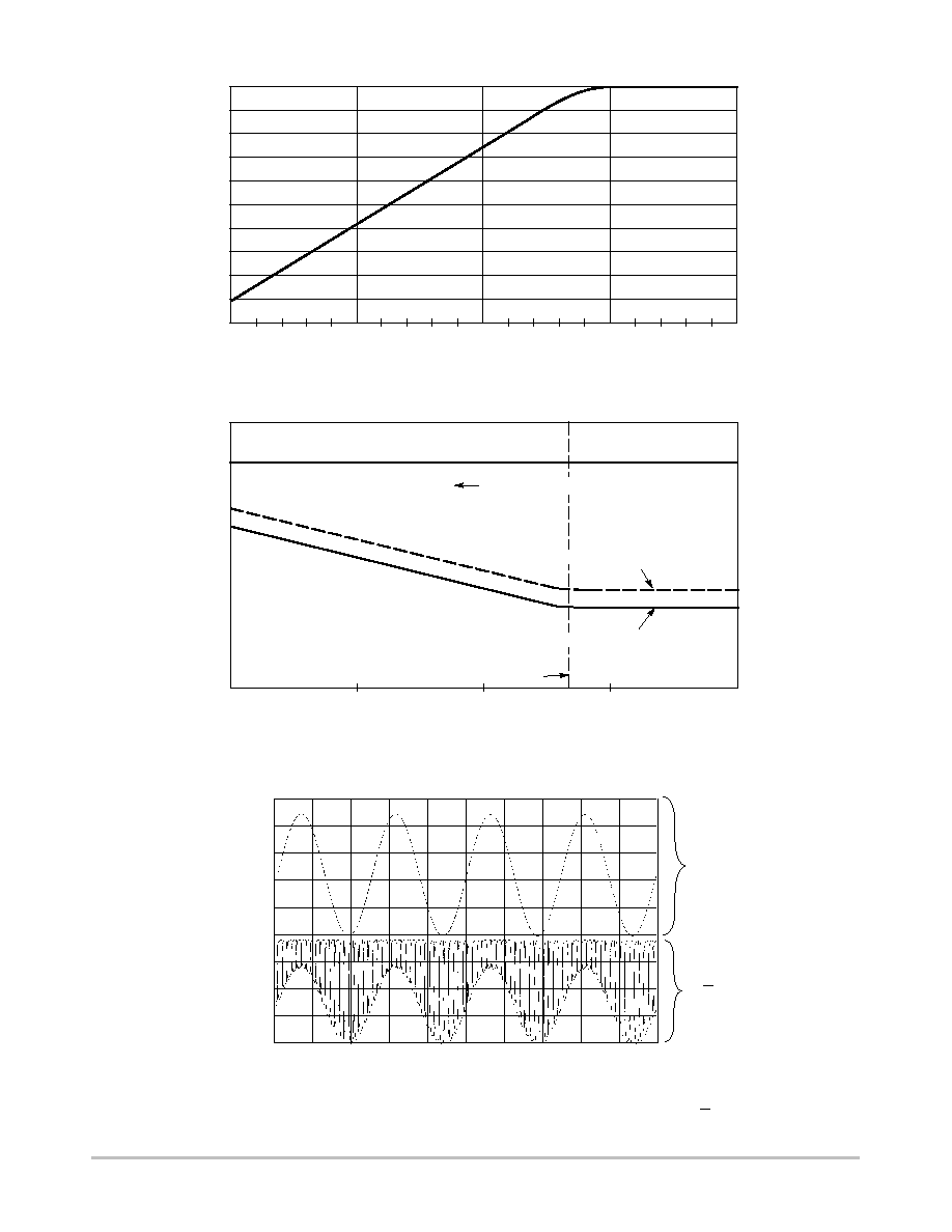
Figure 5. Output Amplitude % vs. V
CTRL
(pin #A3)
V
CTRL
(V)
OUTPUT AMPLITUDE (%)
100
90
80
70
60
50
40
30
20
10
0
V
CC
- 0.0
V
CC
- 0.5
V
CC
- 1.0
V
CC
- 1.5
V
CC
- 2.0
Figure 6. Output Amplitude vs. V
CTRL
(pin #A3)
V
CTRL
(V)
OUTPUT AMPLITUDE
V
OH
V
OL
V
CC
- 1.3
V
CC
- 0.0
V
CC
- 0.5
V
CC
- 1.0
V
CC
- 1.5
V
CC
- 2.0
MIN. AMPLITUDE REGION
MAX. AMPLITUDE REGION
AMPLITUDE DECREASES
Figure 7. Output Response Under Amplitude Modulation of V
CTRL
(Conditions Include V
CC
- V
EE
= 3.3 V at 25
5
C, f
IN
(V
CTRL
) = 200 MHz, and f
IN
(D, D) = 2 GHz)
0
2
4
6
8
10 12 14 16 18 20
1.60
1.80
2.00
2.20
2.40
2.60
2.80
3.00
3.20
3.40
TIME (ns)
V
CTRL
Q/Q
VOL
T
AGE (V)
2.375 V
v
V
CC
- V
EE
< 3.0 V
3.0 V
v
V
CC
- V
EE
v
3.465 V

NBSG16VS
http://onsemi.com
10
INPUT FREQUENCY (GHz)
Figure 8. Output Voltage Amplitude (V
OUTPP
) / RMS Jitter vs.
Input Frequency (f
in
) at Ambient Temperature (Typical)
OUTPUT VOL
T
AGE AMPLITUDE (mV)
JITTER
OUT
ps (RMS)
0
100
200
300
400
500
600
700
800
900
1
2
3
4
5
6
7
8
9
10
11
12
0
1
2
3
4
5
6
7
8
9
RMS JITTER
V
CTRL
= V
CC
- 1 V
OUTPUT P-P SPEC
(AMPLITUDE GUARANTEE)
V
CTRL
= V
CC
- 2 V
V
CTRL
= V
CC
- 0 V
INPUT FREQUENCY (GHz)
100
200
300
400
500
600
700
800
1
2
3
4
5
6
7
8
9
10
11
12
2
3
4
5
6
7
8
9
Figure 9. Output Voltage Amplitude (V
OUTPP
) / RMS Jitter vs.
Input Frequency (f
in
) at Ambient Temperature (Typical)
OUTPUT VOL
T
AGE AMPLITUDE (mV)
0
1
0
RMS JITTER
V
CTRL
= V
CC
- 1 V
OUTPUT P-P SPEC
(AMPLITUDE GUARANTEE)
V
CTRL
= V
CC
- 2 V
V
CTRL
= V
CC
- 0 V
JITTER
OUT
ps (RMS)

NBSG16VS
http://onsemi.com
11
V TT = V CC - 2.0 V
W
Driver
Device
Receiver
Device
Q
D
50
W
50
V TT
Q
D
Figure 10. AC Reference Measurement
D
D
Q
Q
t
PHL
t
PLH
V
INPP
= V
IH
(D) - V
IL
(D)
Figure 11. Typical Termination for Output Driver
and Device Evaluation (Refer to Application Note
AND8020 - Termination of ECL Logic Devices)
V
OUTPP
= V
OH
(Q) - V
OL
(Q)
NBSG16VS
http://onsemi.com
12
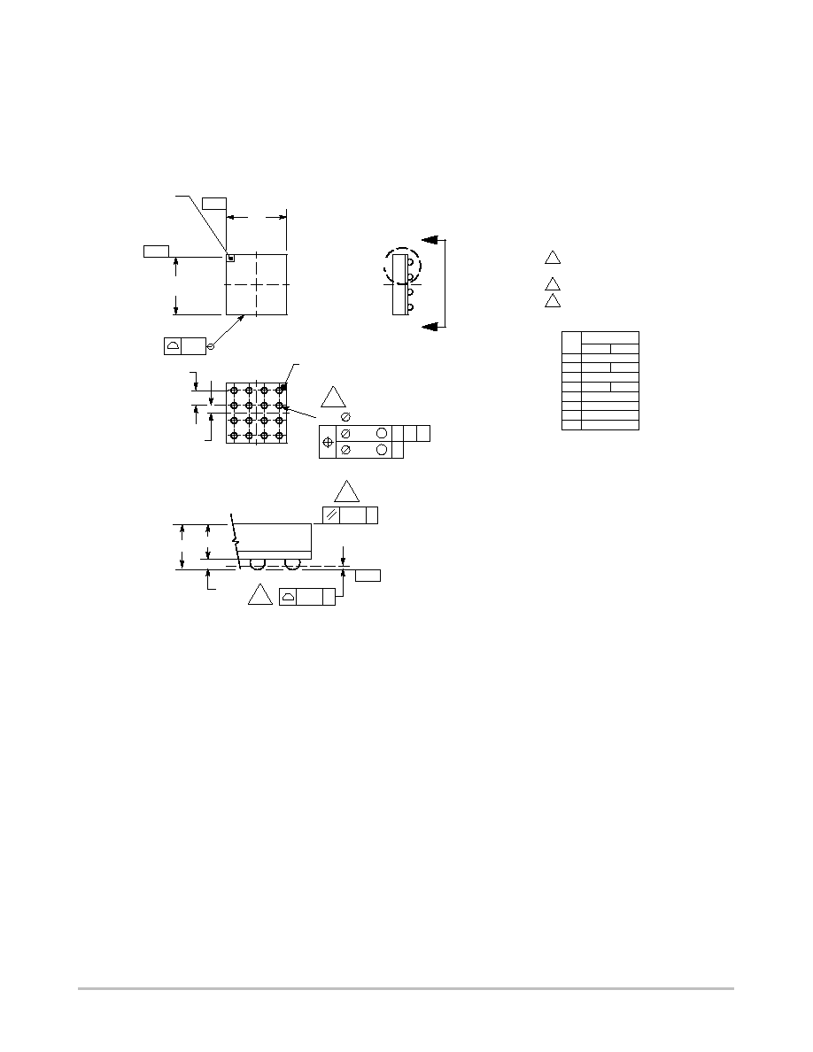
PACKAGE DIMENSIONS
FCBGA-16
BA SUFFIX
PLASTIC 4X4 (mm) BGA FLIP CHIP PACKAGE
CASE 489-01
ISSUE O
0.20
LASER MARK FOR PIN 1
IDENTIFICATION IN
THIS AREA
D
E
M
A1
A2
A
0.10 Z
0.15 Z
ROTATED 90 CLOCKWISE
DETAIL K
_
5
VIEW M-M
e
3 X
S
M
X
0.15
Y
Z
0.08
Z
3
b
16 X
FEDUCIAL FOR PIN A1
IDENTIFICATION IN THIS AREA
4
3
2
1
A
B
C
D
4
16 X
NOTES:
1. DIMENSIONS ARE IN MILLIMETERS.
2. INTERPRET DIMENSIONS AND TOLERANCES
PER ASME Y14.5M, 1994.
3. DIMENSION b IS MEASURED AT THE MAXIMUM
SOLDER BALL DIAMETER, PARALLEL TO DATUM
PLANE Z.
4. DATUM Z (SEATING PLANE) IS DEFINED BY THE
SPHERICAL CROWNS OF THE SOLDER BALLS.
5. PARALLELISM MEASUREMENT SHALL EXCLUDE
ANY EFFECT OF MARK ON TOP SURFACE OF
PACKAGE.
DIM
MIN
MAX
MILLIMETERS
A
1.40 MAX
A1
0.25
0.35
A2
1.20 REF
b
0.30
0.50
D
4.00 BSC
E
4.00 BSC
e
1.00 BSC
S
0.50 BSC
K
-X-
-Y-
M
M
-Z-

NBSG16VS
http://onsemi.com
13
PACKAGE DIMENSIONS
16 PIN QFN
MN SUFFIX
CASE 485G-01
ISSUE O
X
M
0.10 (0.004)
T
-T-
-X-
NOTE 3
SEATING
PLANE
L
A
M
-Y-
B
N
0.25 (0.010) T
0.25 (0.010) T
J
C
K
R
0.08 (0.003) T
G
E
H
F
P
D
Y
1
4
5
8
12
9
16
13
DIM
MIN
MAX
MIN
MAX
INCHES
MILLIMETERS
A
3.00 BSC
0.118 BSC
B
3.00 BSC
0.118 BSC
C
0.80
1.00
0.031
0.039
D
0.23
0.28
0.009
0.011
G
0.50 BSC
0.020 BSC
H
0.875
0.925
0.034
0.036
J
0.20 REF
0.008 REF
K
0.00
0.05
0.000
0.002
L
0.35
0.45
0.014
0.018
NOTES:
1. DIMENSIONING AND TOLERANCING PER ANSI
Y14.5M, 1982.
2. CONTROLLING DIMENSION: MILLIMETERS.
3. DIMENSION D APPLIES TO PLATED TERMINAL
AND IS MEASURED BETWEEN 0.25 AND 0.30 MM
FROM TERMINAL.
4. COPLANARITY APPLIES TO THE EXPOSED PAD
AS WELL AS THE TERMINALS.
E
1.75
1.85
0.069
0.073
F
1.75
1.85
0.069
0.073
M
1.50 BSC
0.059 BSC
N
1.50 BSC
0.059 BSC
P
0.875
0.925
0.034
0.036
R
0.60
0.80
0.024
0.031

NBSG16VS
http://onsemi.com
14
ON Semiconductor and are registered trademarks of Semiconductor Components Industries, LLC (SCILLC). SCILLC reserves the right to make
changes without further notice to any products herein. SCILLC makes no warranty, representation or guarantee regarding the suitability of its products for any
particular purpose, nor does SCILLC assume any liability arising out of the application or use of any product or circuit, and specifically disclaims any and all
liability, including without limitation special, consequential or incidental damages. "Typical" parameters which may be provided in SCILLC data sheets and/or
specifications can and do vary in different applications and actual performance may vary over time. All operating parameters, including "Typicals" must be
validated for each customer application by customer's technical experts. SCILLC does not convey any license under its patent rights nor the rights of others.
SCILLC products are not designed, intended, or authorized for use as components in systems intended for surgical implant into the body, or other applications
intended to support or sustain life, or for any other application in which the failure of the SCILLC product could create a situation where personal injury or death
may occur. Should Buyer purchase or use SCILLC products for any such unintended or unauthorized application, Buyer shall indemnify and hold SCILLC
and its officers, employees, subsidiaries, affiliates, and distributors harmless against all claims, costs, damages, and expenses, and reasonable attorney fees
arising out of, directly or indirectly, any claim of personal injury or death associated with such unintended or unauthorized use, even if such claim alleges that
SCILLC was negligent regarding the design or manufacture of the part. SCILLC is an Equal Opportunity/Affirmative Action Employer.
PUBLICATION ORDERING INFORMATION
JAPAN: ON Semiconductor, Japan Customer Focus Center
2-9-1 Kamimeguro, Meguro-ku, Tokyo, Japan 153-0051
Phone: 81-3-5773-3850
Email: r14525@onsemi.com
ON Semiconductor Website: http://onsemi.com
For additional information, please contact your local
Sales Representative.
NBSG16VS/D
Literature Fulfillment:
Literature Distribution Center for ON Semiconductor
P.O. Box 5163, Denver, Colorado 80217 USA
Phone: 303-675-2175 or 800-344-3860 Toll Free USA/Canada
Fax: 303-675-2176 or 800-344-3867 Toll Free USA/Canada
Email: ONlit@hibbertco.com
N. American Technical Support: 800-282-9855 Toll Free USA/Canada