 | –≠–ª–µ–∫—Ç—Ä–æ–Ω–Ω—ã–π –∫–æ–º–ø–æ–Ω–µ–Ω—Ç: NBSG72AMN | –°–∫–∞—á–∞—Ç—å:  PDF PDF  ZIP ZIP |

©
Semiconductor Components Industries, LLC, 2004
October, 2004 - Rev. 2
1
Publication Order Number:
NBSG72A/D
NBSG72A
2.5V/3.3V SiGe Differential
2 X 2 Crosspoint Switch
with Output Level Select
The NBSG72A is a high-bandwidth fully differential 2 X 2
crosspoint switch with Output Level Select (OLS) capabilities. This is
a part of the GigaComm
TM
family of high performance Silicon
Germanium products. The device is housed in a low profile 3 X 3 mm
16-pin QFN package.
Differential inputs incorporate internal 50
W termination resistors
and accept NECL (Negative ECL), PECL (Positive ECL),
LVCMOS/LVTTL, CML, or LVDS. The OLS input is used to
program the peak-to-peak output amplitude between 0 mV and
800 mV in five discrete steps. The SELECT inputs are single-ended
and can be driven with either LVECL or LVCMOS/LVTTL
input levels.
∑
Maximum Input Clock Frequency > 7 GHz Typical
∑
Maximum Input Data Rate > 7 Gb/s Typical
∑
200 ps Typical Propagation Delay (OLS = FLOAT)
∑
55/45 ps Typical Rise/Fall Times (OLS = FLOAT)
∑
Selectable Swing PECL Output with Operating Range:
V
CC
= 2.375 V to 3.465 V with V
EE
= 0 V
∑
Selectable Swing NECL Output with NECL Inputs with
Operating Range: V
CC
= 0 V with V
EE
= -2.375 V to -3.465 V
∑
Selectable Output Levels (0 mV, 200 mV, 400 mV, 600 mV or
800 mV Peak-to-Peak Output)
∑
50
W Internal Input Termination Resistors
∑
Single-Ended LVECL or LVCMOS/LVTTL Select Inputs
(SELA, SELB)
∑
Pb-Free Package is Available
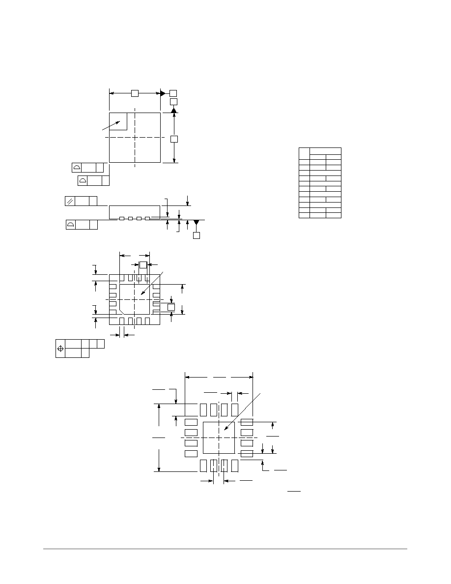
A
= Assembly Location
L
= Wafer Lot
Y
= Year
W
= Work Week
*For additional marking information, refer to
Application Note AND8002/D.
MARKING
DIAGRAM*
QFN-16
MN SUFFIX
CASE 485G
http://onsemi.com
See detailed ordering and shipping information in the package
dimensions section on page 13 of this data sheet.
ORDERING INFORMATION
16
SG
72A
ALYW
1
««
««
1
NBSG72A
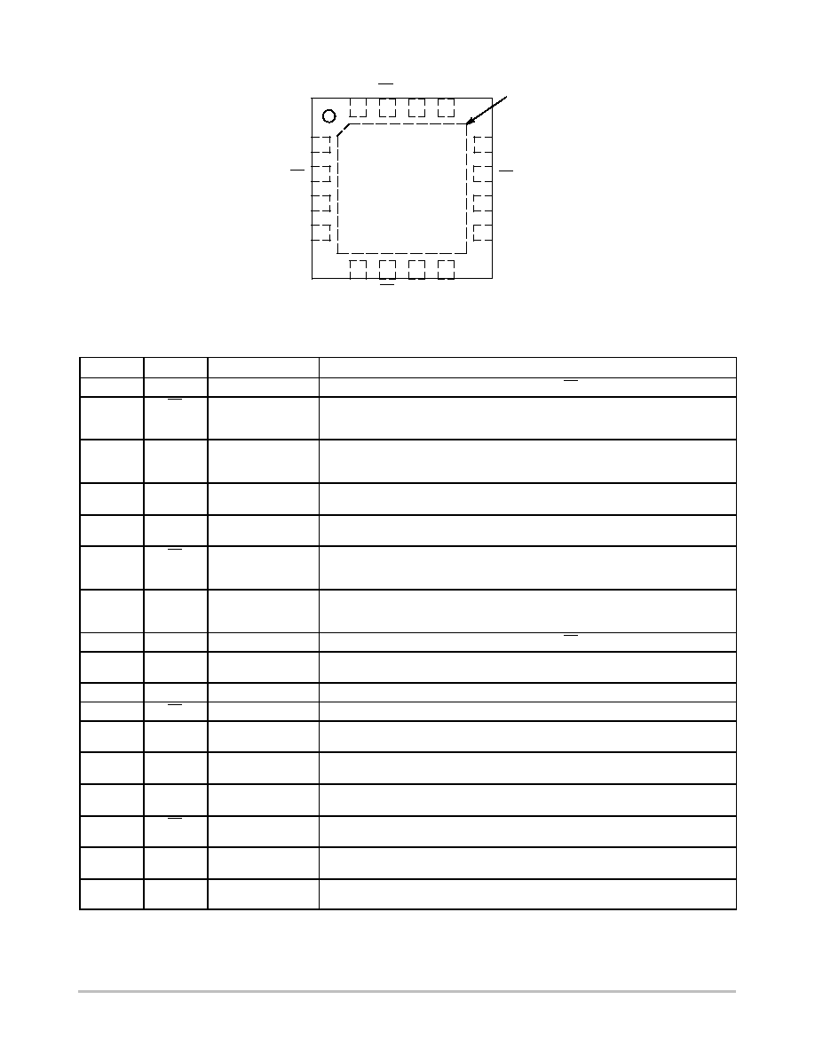
http://onsemi.com
2
Figure 1. QFN-16 Pinout (Top View)
V
EE
D1
D1
V
TD1
V
CC
Q0
Q0
OLS
V
CC
Q1
Q1
SELB
V
TD0
D0
D0
SELA
5
6
7
8
16
15
14
13
12
11
10
9
1
2
3
4
NBSG72A
Exposed Pad (EP)
Table 1. PIN DESCRIPTION
Pin No.
Name
I/O
Description
1
VTD0
-
Common Internal 50
W
Termination Pin for D0 and D0 Input. See Table 4. (Note 1)
2
D0
LVDS, CML, ECL,
LVTTL, LVCMOS
Input
Inverted Differential Input 0.
3
D0
LVDS, CML, ECL,
LVTTL, LVCMOS
Input
Noninverted Differential Input 0.
4
SELA
LVECL, LVCMOS
Input
Select Logic Input A. Internal 75 k
W
Pulldown to V
EE
.
5
V
EE
-
Negative Supply. All V
EE
Pins must be Externally Connected to Power Supply to
Guarantee Proper Operation.
¡¡¡¡¡
¡
¡¡¡
¡
¡¡¡¡¡
6
¡¡¡¡
¡
¡¡
¡
¡¡¡¡
D1
LVDS, CML, ECL,
LVTTL, LVCMOS
Input
¡¡¡¡¡¡¡¡¡¡¡¡¡¡¡¡¡¡¡¡¡
¡
¡¡¡¡¡¡¡¡¡¡¡¡¡¡¡¡¡¡¡
¡
¡¡¡¡¡¡¡¡¡¡¡¡¡¡¡¡¡¡¡¡¡
Inverted Differential Input 1.
¡¡¡¡¡
¡
¡¡¡
¡
¡¡¡¡¡
7
¡¡¡¡
¡
¡¡
¡
¡¡¡¡
D1
LVDS, CML, ECL,
LVTTL, LVCMOS
Input
¡¡¡¡¡¡¡¡¡¡¡¡¡¡¡¡¡¡¡¡¡
¡
¡¡¡¡¡¡¡¡¡¡¡¡¡¡¡¡¡¡¡
¡
¡¡¡¡¡¡¡¡¡¡¡¡¡¡¡¡¡¡¡¡¡
Noninverted Differential Input 1.
8
VTD1
-
Common Internal 50
W
Termination Pin for D1 and D1 Input. See Table 4. (Note 1)
¡¡¡¡¡
¡
¡¡¡
¡
¡¡¡¡¡
9
¡¡¡¡
¡
¡¡
¡
¡¡¡¡
SELB
LVECL, LVCMOS
Input
¡¡¡¡¡¡¡¡¡¡¡¡¡¡¡¡¡¡¡¡¡
¡
¡¡¡¡¡¡¡¡¡¡¡¡¡¡¡¡¡¡¡
¡
¡¡¡¡¡¡¡¡¡¡¡¡¡¡¡¡¡¡¡¡¡
Select Logic Input B. Internal 75 k
W
Pulldown to V
EE
.
¡¡¡¡¡
¡¡¡¡¡
10
¡¡¡¡
¡¡¡¡
Q1
RSECL Output
¡¡¡¡¡¡¡¡¡¡¡¡¡¡¡¡¡¡¡¡¡
¡¡¡¡¡¡¡¡¡¡¡¡¡¡¡¡¡¡¡¡¡
Noninverted Differential Output.
11
Q1
RSECL Output
Inverted Differential Output.
¡¡¡¡¡
¡¡¡¡¡
12
¡¡¡¡
¡¡¡¡
V
CC
-
¡¡¡¡¡¡¡¡¡¡¡¡¡¡¡¡¡¡¡¡¡
¡¡¡¡¡¡¡¡¡¡¡¡¡¡¡¡¡¡¡¡¡
Positive Supply. All V
CC
Pins must be Externally Connected to Power Supply to
Guarantee Proper Operation.
¡¡¡¡¡
¡
¡¡¡
¡
¡¡¡¡¡
13
¡¡¡¡
¡
¡¡
¡
¡¡¡¡
OLS
(Note 2)
Input
¡¡¡¡¡¡¡¡¡¡¡¡¡¡¡¡¡¡¡¡¡
¡
¡¡¡¡¡¡¡¡¡¡¡¡¡¡¡¡¡¡¡
¡
¡¡¡¡¡¡¡¡¡¡¡¡¡¡¡¡¡¡¡¡¡
Input Pin for Output Level Select (OLS) See Table 3.
14
Q0
RSECL Output
Noninverted Differential Output Typically Terminated with 50
W
Resistor to
V
TT
= V
CC
- 2.0 V.
¡¡¡¡¡
¡
¡¡¡
¡
¡¡¡¡¡
15
¡¡¡¡
¡
¡¡
¡
¡¡¡¡
Q0
RSECL Output
¡¡¡¡¡¡¡¡¡¡¡¡¡¡¡¡¡¡¡¡¡
¡
¡¡¡¡¡¡¡¡¡¡¡¡¡¡¡¡¡¡¡
¡
¡¡¡¡¡¡¡¡¡¡¡¡¡¡¡¡¡¡¡¡¡
Inverted Differential Output Typically Terminated with 50
W
Resistor to
V
TT
= V
CC
- 2.0 V.
¡¡¡¡¡
¡¡¡¡¡
16
¡¡¡¡
¡¡¡¡
V
CC
-
¡¡¡¡¡¡¡¡¡¡¡¡¡¡¡¡¡¡¡¡¡
¡¡¡¡¡¡¡¡¡¡¡¡¡¡¡¡¡¡¡¡¡
Positive Supply. All V
CC
Pins must be Externally Connected to Power Supply to
Guarantee Proper Operation.
-
EP
-
Exposed Pad. The thermally exposed pad on package bottom (see case drawing)
must be attached to a heat-sinking conduit.
1. In the differential configuration when the input termination pins (VTD0, VTD1) are connected to a common termination voltage, and if no signal
is applied then the device will be susceptible to self-oscillation.
2. When an output level of 400 mV is desired and V
CC
- V
EE
> 3.0 V, 2 k
W
resistor should be connected from OLS pin to V
EE
.

NBSG72A
http://onsemi.com
3
Q0
Q0
LOW
D0
HIGH
D1
LOW
D0
HIGH
D1
SELA
Q0
Figure 2. Logic/Block Diagram
LOW
LOW
HIGH
HIGH
SELB
D0
D0
D1
D1
Q1
VTD0
D0
SELA
SELB
OLS
Q1
2
2
2
2
2
2
2
2
2
2
V
CC
V
EE
+
50
W
50
W
75 k
W
75 k
W
Table 2. TRUTH TABLE
Q1
D0
50
W
VTD1
D1
D1
50
W
Table 3. OUTPUT LEVEL SELECT (OLS)
OLS
Output Amplitude (V
OUTPP
)
OLS Sensitivity
V
CC
800 mV
OLS - 75 mV
V
CC
- 0.4 V
200 mV
OLS
±
150 mV
V
CC
- 0.8 V
600 mV
OLS
±
100 mV
V
CC
- 1.2 V
0
OLS
±
75 mV
V
EE
(Note 3)
400 mV
OLS
±
100 mV
FLOAT
600 mV
N/A
3. When an output level of 400 mV is desired and V
CC
- V
EE
> 3.0 V, a 2 k
W
resistor should be connected from OLS to V
EE
.
Table 4. INTERFACING OPTIONS
Interfacing Options
Connections
CML
Connect VTD0 and VTD1 to V
CC
LVDS
VTD0 and VTD1 Should Be Left Floating.
AC-COUPLED
Bias VTD0 and VTD1 Inputs within Common Mode Range (VIHCMR)
RSECL, PECL, NECL
Standard ECL Termination Techniques
LVCMOS / LVTTL
The external voltage should be applied to the unused complementary differential input.
Nominal voltage is 1.5 V for LVTTL and V
CC
/2 for LVCMOS Inputs.
NBSG72A
http://onsemi.com
4
Table 5. ATTRIBUTES
Characteristics
Value
Internal Input Pulldown Resistor (SELA, SELB)
75 k
W
ESD Protection
Human Body Model
Machine Model
Charged Device Model
> 2 kV
> 50 V
> 1 kV
Moisture Sensitivity (Note 1)
Level 1
Flammability Rating
Oxygen Index: 28 to 34
UL 94 V-0 @ 0.125 in
Transistor Count
436
Meets or exceeds JEDEC Spec EIA/JESD78 IC Latchup Test
1. For additional information, see Application Note AND8003/D.
Table 6. MAXIMUM RATINGS
Symbol
Parameter
Condition 1
Condition 2
Rating
Units
V
CC
Positive Power Supply
V
EE
= 0 V
3.6
V
V
EE
Negative Power Supply
V
CC
= 0 V
-3.6
V
V
I
Positive Input
Negative Input
V
EE
= 0 V
V
CC
= 0 V
V
I
V
CC
V
I
V
EE
3.6
-3.6
V
V
V
INPP
Differential Input Voltage |D
X
- D
X
|
V
EE
- V
CC
w
2.8 V
V
EE
- V
CC
t
2.8 V
2.8
|V
CC
- V
EE
|
V
I
out
Output Current
Continuous
Surge
25
50
mA
mA
I
IN
Input Current Through R
T
(50
W
Resistor)
Static
Surge
45
80
mA
mA
T
A
Operating Temperature Range
-40 to +85
∞
C
T
stg
Storage Temperature Range
-65 to +150
∞
C
q
JA
Thermal Resistance (Junction-to-Ambient)
(Note 2)
0 lfpm
500 lfpm
QFN-16
QFN-16
42
35
∞
C/W
∞
C/W
q
JC
Thermal Resistance (Junction-to-Case)
(Note 2)
QFN-16
4
∞
C/W
T
sol
Wave Solder
< 15 sec
225
∞
C
Maximum ratings are those values beyond which device damage can occur. Maximum ratings applied to the device are individual stress limit
values (not normal operating conditions) and are not valid simultaneously. If these limits are exceeded, device functional operation is not implied,
damage may occur and reliability may be affected.
2. JEDEC standard multilayer board - 1S2P (1 signal, 2 power).
NBSG72A
http://onsemi.com
5
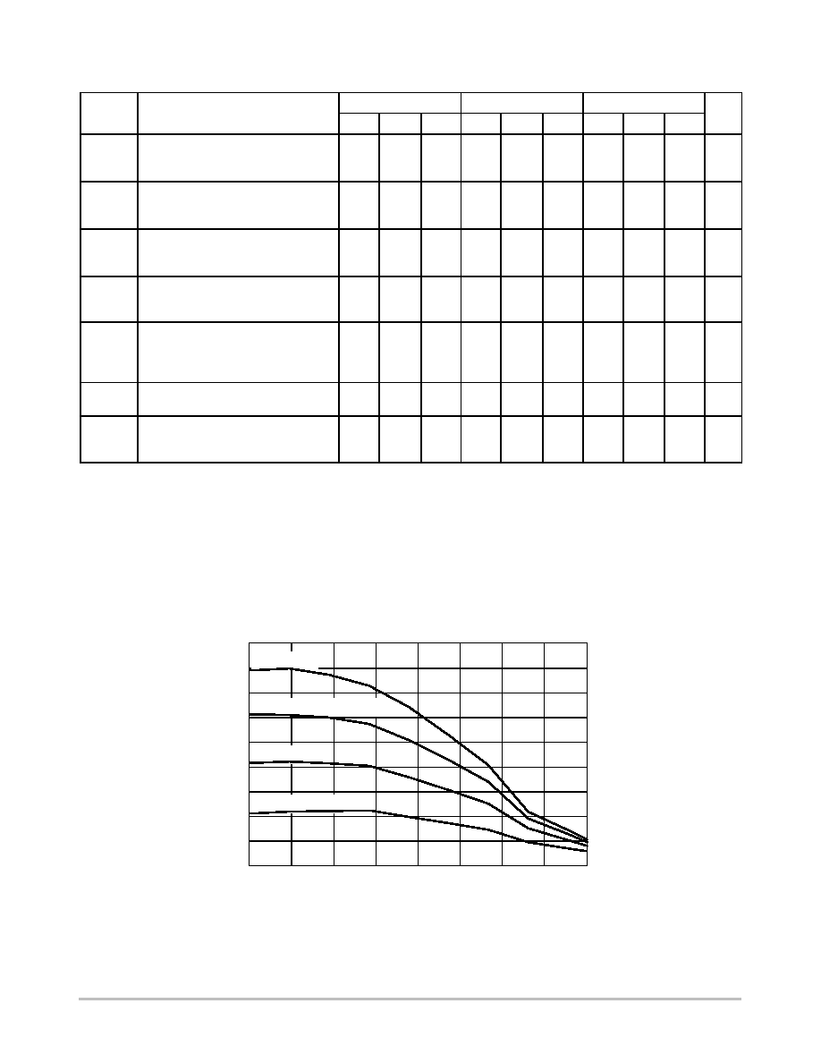
Table 7. DC CHARACTERISTICS, INPUT WITH PECL OUTPUT
V
CC
= 2.5 V; V
EE
= 0 V (Note 3)
-40
∞
C
25
∞
C
85
∞
C
Symbol
Characteristic
Min
Typ
Max
Min
Typ
Max
Min
Typ
Max
Unit
I
EE
Negative Power Supply Current
40
55
65
40
55
65
40
55
65
mA
V
OH
Output HIGH Voltage (Note 4)
1460
1510
1560
1490
1540
1590
1515
1565
1615
mV
V
OL
Output LOW Voltage (Note 4)
(OLS = V
CC
)
(OLS = V
CC
- 0.4 V)
(OLS = V
CC
- 0.8 V, OLS = FLOAT)
(OLS = V
CC
- 1.2 V)
(OLS = V
EE
)
555
1235
775
1455
1005
705
1295
895
1505
1095
855
1355
1015
1555
1185
595
1270
810
1490
1040
745
1330
930
1540
1130
895
1390
1050
1590
1220
625
1295
840
1510
1065
775
1355
960
1560
1155
925
1415
1080
1610
1245
mV
V
OUTPP
Output Voltage Amplitude
(OLS = V
CC
)
(OLS = V
CC
- 0.4 V)
(OLS = V
CC
- 0.8 V, OLS = FLOAT)
(OLS = V
CC
- 1.2 V)
(OLS = V
EE
)
700
125
525
0
325
800
215
615
5
415
680
120
520
0
320
795
210
610
0
410
680
120
515
0
320
790
210
605
5
410
mV
V
IH
Input HIGH Voltage (Single-Ended)
(Note 6)
D0, D0, D1, D1
V
EE
+
1275
V
CC
-
1000*
V
CC
V
EE
+
1275
V
CC
-
1000*
V
CC
V
EE
+
1275
V
CC
-
1000*
V
CC
mV
V
IL
Input LOW Voltage (Single-Ended)
(Note 7)
D0, D0, D1, D1
V
EE
V
CC
-
1400*
V
IH
-
150
V
EE
V
CC
-
1400*
V
IH
-
150
V
EE
V
CC
-
1400*
V
IH
-
150
mV
V
IHCMR
Input HIGH Voltage Common Mode
Range (Differential Configuration) (Note 5)
1.2
2.5
1.2
2.5
1.2
2.5
V
R
TIN
Internal Input Termination Resistor
45
50
55
45
50
55
45
50
55
W
I
IH
Input HIGH Current (@V
IH
)
35
100
35
100
35
100
m
A
I
IL
Input LOW Current (@V
IL
)
20
100
20
100
20
100
m
A
NOTE: Device will meet the specifications after thermal equilibrium has been established when mounted in a test socket or printed circuit
board with maintained transverse airflow greater than 500 lfpm. Electrical parameters are guaranteed only over the declared
operating temperature range. Functional operation of the device exceeding these conditions is not implied. Device specification limit
values are applied individually under normal operating conditions and not valid simultaneously.
*Typicals used for testing purposes.
3. Input and output parameters vary 1:1 with V
CC
. V
EE
can vary +0.125 V to -0.965 V.
4. All loading with 50
W
to V
CC
- 2.0 V.
5. V
IHCMR
min varies 1:1 with V
EE
, V
IHCMR
max varies 1:1 with V
CC
. The V
IHCMR
range is referenced to the most positive side of the differential
input signal.
6. V
IH
cannot exceed V
CC
.
7. V
IL
always
w
V
EE
.

NBSG72A
http://onsemi.com
6
Table 8. DC CHARACTERISTICS, INPUT WITH PECL OUTPUT
V
CC
= 3.3 V; V
EE
= 0 V (Note 8)
-40
∞
C
25
∞
C
85
∞
C
Symbol
Characteristic
Min
Typ
Max
Min
Typ
Max
Min
Typ
Max
Unit
I
EE
Negative Power Supply Current
40
55
65
40
55
65
40
55
65
mA
V
OH
Output HIGH Voltage (Note 9)
2260
2310
2360
2290
2340
2390
2315
2365
2415
mV
V
OL
Output LOW Voltage (Note 9)
(OLS = V
CC
)
(OLS = V
CC
- 0.4 V)
(OLS = V
CC
- 0.8 V, OLS = FLOAT)
(OLS = V
CC
- 1.2 V)
**(OLS = V
EE
)
1320
2030
1550
2260
1785
1470
2090
1670
2310
1875
1620
2150
1790
2360
1965
1360
2065
1585
2290
1820
1510
2125
1705
2340
1910
1660
2185
1825
2390
2000
1390
2090
1615
2315
1850
1540
2150
1735
2365
1940
1690
2210
1855
2415
2030
mV
V
OUTPP
Output Amplitude Voltage
(OLS = V
CC
)
(OLS = V
CC
- 0.4 V)
(OLS = V
CC
- 0.8 V, OLS = FLOAT)
(OLS = V
CC
- 1.2 V)
**(OLS = V
EE
)
715
130
550
0
345
815
220
640
0
435
705
125
545
0
340
805
215
635
0
430
690
125
540
0
335
800
215
630
0
425
mV
V
IH
Input HIGH Voltage (Single-Ended)
(Note 11)
D0, D0, D1, D1
V
EE
+
1275
V
CC
-
1000*
V
CC
V
EE
+
1275
V
CC
-
1000*
V
CC
V
EE
+
1275
V
CC
-
1000*
V
CC
mV
V
IL
Input LOW Voltage (Single-Ended)
(Note 12)
D0, D0, D1, D1
V
IH
-
2600
V
CC
-
1400*
V
IH
-
150
V
IH
-
2600
V
CC
-
1400*
V
IH
-
150
V
IH
-
2600
V
CC
-
1400*
V
IH
-
150
mV
V
IHCMR
Input HIGH Voltage Common Mode
Range (Differential Configuration)
(Note 10)
1.2
3.3
1.2
3.3
1.2
3.3
V
R
TIN
Internal Input Termination Resistor
45
50
55
45
50
55
45
50
55
W
I
IH
Input HIGH Current (@V
IH
)
35
100
35
100
35
100
m
A
I
IL
Input LOW Current (@V
IL
)
20
100
20
100
20
100
m
A
NOTE: Device will meet the specifications after thermal equilibrium has been established when mounted in a test socket or printed circuit
board with maintained transverse airflow greater than 500 lfpm. Electrical parameters are guaranteed only over the declared
operating temperature range. Functional operation of the device exceeding these conditions is not implied. Device specification limit
values are applied individually under normal operating conditions and not valid simultaneously.
*Typicals used for testing purposes.
**When an output level of 400 mV is desired and V
CC
- V
EE
> 3.0 V, a 2 k
W
resistor should be connected from OLS to V
EE
.
8. Input and output parameters vary 1:1 with V
CC
. V
EE
can vary +0.925 V to -0.165 V.
9. All loading with 50
W
to V
CC
- 2.0 V.
10. V
IHCMR
min varies 1:1 with V
EE
, V
IHCMR
max varies 1:1 with V
CC
. The V
IHCMR
range is referenced to the most positive side of the differential
input signal.
11. V
IH
cannot exceed V
CC
.
12. V
IL
always
w
V
EE
.
NBSG72A
http://onsemi.com
7
Table 9. DC CHARACTERISTICS, NECL INPUT WITH NECL OUTPUT
V
CC
= 0 V; V
EE
= -3.465 V to -2.375 V (Note 13)
-40
∞
C
25
∞
C
85
∞
C
Symbol
Characteristic
Min
Typ
Max
Min
Typ
Max
Min
Typ
Max
Unit
I
EE
Negative Power Supply Current
40
55
65
40
55
65
40
55
65
mA
V
OH
Output HIGH Voltage (Note 14)
-1040
-990
-840
-1010
-960
-910
-985
-935
-885
mV
V
OL
Output LOW Voltage (Note 14)
-3.465 V
v
V
EE
v
-3.0 V
(OLS = V
CC
)
(OLS = V
CC
- 0.4 V)
(OLS = V
CC
- 0.8 V, OLS =FLOAT)
(OLS = V
CC
- 1.2 V)
**(OLS = V
EE
)
-3.0 V < V
EE
v
-2.375 V
(OLS = V
CC
)
(OLS = V
CC
- 0.4 V)
(OLS = V
CC
- 0.8 V, OLS =FLOAT)
(OLS = V
CC
- 1.2 V)
(OLS = V
EE
)
-1980
-1270
-1750
-1040
-1515
-1945
-1265
-1725
-1045
-1495
-1830
-1210
-1630
-990
-1425
-1795
-1205
-1605
-995
-1405
-1680
-1150
-1510
-940
-1335
-1645
-1145
-1485
-945
-1315
-1940
-1235
-1715
-1010
-1480
-1905
-1230
-1690
-1010
-1460
-1790
-1175
-1595
-960
-1390
-1755
-1170
-1570
-960
-1370
-1640
-1115
-1475
-910
-1300
-1605
-1110
-1450
-910
-1280
-1910
-1210
-1685
-985
-1450
-1875
-1205
-1660
-990
-1435
-1760
-1150
-1565
-935
-1360
-1725
-1145
-1540
-940
-1345
-1610
-1090
-1445
-885
-1270
-1575
-1085
-1420
-890
-1255
mV
V
OUTPP
Output Voltage Amplitude
-3.465 V
v
V
EE
v
-3.0 V
(OLS = V
CC
)
(OLS = V
CC
- 0.4 V)
(OLS = V
CC
- 0.8 V, OLS = FLOAT)
(OLS = V
CC
- 1.2 V)
**(OLS = V
EE
)
-3.0 V < V
EE
v
-2.375 V
(OLS = V
CC
)
(OLS = V
CC
- 0.4 V)
(OLS = V
CC
- 0.8 V, OLS =FLOAT)
(OLS = V
CC
- 1.2 V)
(OLS = V
EE
)
715
130
550
0
345
700
125
525
0
325
815
220
640
0
435
800
215
615
5
415
705
125
545
0
340
690
120
520
0
320
805
215
635
0
430
795
210
610
0
410
690
125
540
0
335
680
120
515
0
320
800
215
630
0
425
790
210
605
5
410
mV
V
IH
Input HIGH Voltage (Single-Ended)
(Note 16)
D0, D0, D1, D1
V
EE
+
1275
V
CC
-
1000*
V
CC
V
EE
+
1275
V
CC
-
1000*
V
CC
V
EE
+
1275
V
CC
-
1000*
V
CC
mV
V
IL
Input LOW Voltage (Single-Ended)
(Note 17)
D0, D0, D1, D1
V
IH
-
2600
V
CC
-
1400*
V
IH
-
150
V
IH
-
2600
V
CC
-
1400*
V
IH
-
150
V
IH
-
2600
V
CC
-
1400*
V
IH
-
150
mV
V
IHCMR
Input HIGH Voltage Common Mode
Range (Differential Configuration)
(Note 15)
V
EE
+1.2
0.0
V
EE
+1.2
0.0
V
EE
+1.2
0.0
V
R
TIN
Internal Input Termination Resistor
45
50
55
45
50
55
45
50
55
W
I
IH
Input HIGH Current (@V
IH
)
35
100
35
100
35
100
m
A
I
IL
Input LOW Current (@V
IL
)
20
100
20
100
20
100
m
A
I
OLS
OLS Input Current (See Figure 9)
(OLS = V
CC
)
(OLS = V
CC
- 0.4 V)
(OLS = V
CC
- 0.8 V, OLS = FLOAT)
(OLS = V
CC
- 1.2 V)
-3.0 V < V
EE
v
-2.375 V
(OLS = V
EE
)
-3.465 V
v
V
EE
v
-3.0 V
*(OLS = V
EE
)
-300
-1000
-1500
300
100
5
-100
-400
-600
900
300
100
-300
-1000
-1500
300
100
5
-100
-400
-600
900
300
100
-300
-1000
-1500
300
100
5
-100
-400
-600
900
300
100
m
A
NOTE: Device will meet the specifications after thermal equilibrium has been established when mounted in a test socket or printed circuit
board with maintained transverse airflow greater than 500 lfpm. Electrical parameters are guaranteed only over the declared
operating temperature range. Functional operation of the device exceeding these conditions is not implied. Device specification limit
values are applied individually under normal operating conditions and not valid simultaneously.
*Typicals used for testing purposes.
**When an output level of 400 mV is desired and V
CC
- V
EE
> 3.0 V, a 2 k
W
resistor should be connected from OLS to V
EE
.
13. Input and output parameters vary 1:1 with V
CC
.
14. All loading with 50
W
to V
CC
- 2.0 V.
15. V
IHCMR
min varies 1:1 with V
EE
, V
IHCMR
max varies 1:1 with V
CC
. The V
IHCMR
range is referenced to the most positive side of the differential
input signal.
16. V
IH
cannot exceed V
CC
.
17. V
IL
always
w
V
EE
.
NBSG72A
http://onsemi.com
8
Table 10. AC CHARACTERISTICS
V
CC
= 0 V; V
EE
= -3.465 V to -2.375 V or V
CC
= 2.375 V to 3.465 V; V
EE =
0 V (Note 18)
-40
∞
C
25
∞
C
85
∞
C
Symbol
Characteristic
Min
Typ
Max
Min
Typ
Max
Min
Typ
Max
Unit
V
OUTPP
Output Voltage Amplitude
f
in
< 5 GHz
(Note 18)
f
in
v
7 GHz
400
200
590
250
450
180
590
250
440
130
590
250
mV
t
PLH
Propagation Delay to Output Differential
D0, D1
Q0, Q1
SELA, SELB
Q0, Q1
170
190
205
265
255
350
170
190
205
265
255
350
170
190
210
265
260
350
ps
t
PHL
Propagation Delay to Output Differential
D0, D1
Q0, Q1
SELA, SELB
Q0, Q1
170
150
205
215
255
270
170
150
205
215
255
270
170
150
210
215
260
270
ps
t
SKEW
Duty Cycle Skew (Note 19)
Within-Device Skew
Device-to-Device Skew
5.0
5.0
15
25
25
50
5.0
5.0
15
25
25
50
5.0
5.0
15
25
25
50
ps
t
JITTER
RMS Random Clock Jitter (Note 20)
f
in
v
7 GHz
Peak-to-Peak Data Dependent Jitter
(Note 21)
f
in
v
7 Gb/s
0.2
12
1.5
18
0.2
12
1.5
18
0.2
12
1.5
18
ps
V
INPP
Input Voltage Swing/Sensitivity
(Differential Configuration) (Note 22)
75
2600
75
2600
75
2600
mV
t
r
t
f
Output Rise/Fall Times
(Q0, Q1)
(20% - 80%)
t
r
@ 1 GHz
t
f
40
30
55
45
70
55
40
30
55
45
70
55
40
30
55
45
70
55
ps
NOTE: Device will meet the specifications after thermal equilibrium has been established when mounted in a test socket or printed circuit
board with maintained transverse airflow greater than 500 lfpm. Electrical parameters are guaranteed only over the declared
operating temperature range. Functional operation of the device exceeding these conditions is not implied. Device specification limit
values are applied individually under normal operating conditions and not valid simultaneously.
18. Measured using a 75 mV source, 50% duty cycle clock source. All loading with 50
W
to V
CC
- 2.0 V. OLS = FLOAT. Input edge rates 40 ps
(20% - 80%).
19. t
SKEW
= |t
PLH
- t
PHL
| for a nominal 50% differential clock input waveform.
20. Additive RMS jitter with 50% Duty Cycle clock signal at 7 GHz.
21. Additive Peak-to-Peak data dependent jitter with NRZ PRBS 2
31-1
data at 7 Gb/s.
22. Input Voltage Swing is a single-ended measurement operating in differential mode. V
INPP
(max) cannot exceed V
CC
- V
EE
.
0
100
200
300
400
500
600
700
800
900
1
2
3
4
5
6
7
8
9
INPUT FREQUENCY (GHz)
Figure 3. Output Voltage Amplitude (V
OUTPP
) vs.
Input Clock Frequency (f
in
) @ Ambient Temperature (Typical)
OUTPUT VOL
T
AGE AMPLITUDE (mV)
OLS = V
CC
OLS = V
CC
- 0.8 V = FLOAT
*OLS = V
EE
OLS = V
CC
- 0.4 V
*When an output level of 400 mV is desired and V
CC
- V
EE
> 3.0 V, a 2 k
W
resistor should be connected from OLS to V
EE
.
NBSG72A
http://onsemi.com
9
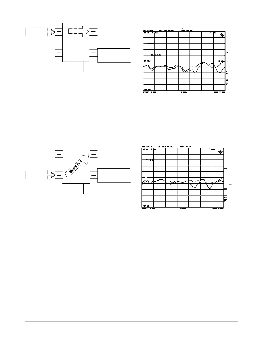
D0
Q0
Q1
D1
Non-Driven
Input
Q1
D1
D0
Signal Path
Measured
Non-Driven Output
(VNA)
Input Signal
Q0
Logic
Low
Logic
High
NBSG72A
Figure 4. Channel-to-Channel Crosstalk Isolation at Ambient Temperature
(D0 to Q0 Signal Path Selected; SelA = Low, SelB = High)
X
scale
= 1 GHz/div
Y
scale
= 10 dB/div
0 dB
Q
Q
Selected
Output
SELA
SELB
1
8
-80
0
20
D0
Q1
D1
Non-Driven
Input
Q1
D1
D0
Input Signal
Q0
Logic
High
Logic
Low
NBSG72A
Figure 5. Channel-to-Channel Crosstalk Isolation at Ambient Temperature
(D1 to Q0 Signal Path Selected; SelA = High, SelB = Low)
X
scale
= 1 GHz/div
Y
scale
= 10 dB/div
0 dB
Q
Q
Q0
Selected
Output
SELA
SELB
-80
0
20
Measured
Non-Driven Output
(VNA)
1
8
NBSG72A
http://onsemi.com
10
D0
Q1
D1
Non-Driven
Input
Q1
D1
D0
Input Signal
Q0
Logic
Low
Logic
Low
NBSG72A
Figure 6. Channel-to-Channel Crosstalk Isolation at Ambient Temperature
(D0 to Q0 and Q1 Signal Path Selected; SelA = Low, SelB = Low)
X
scale
= 1 GHz/div
Y
scale
= 10 dB/div
0dB
Q
Q
Q0
Non-Driven
Selected Output
Signal Path
SELA
SELB
-80
0
20
1
8
Measured Output
(VNA)
D0
Q1
D1
Non-Driven
Input
Q1
D1
D0
Input Signal
Q0
Logic
High
Logic
High
NBSG72A
Figure 7. Channel-to-Channel Crosstalk Isolation at Ambient Temperature
(D1 to Q0 and Q1 Signal Path Selected; SelA = High, SelB = High)
X
scale
= 1 GHz/div
Y
scale
= 10 dB/div
0dB
Q
Q
Q0
Non-Driven
Selected Output
Signal Path
SELA
SELB
Measured Output
(VNA)
-80
0
20
1
8

NBSG72A
http://onsemi.com
11
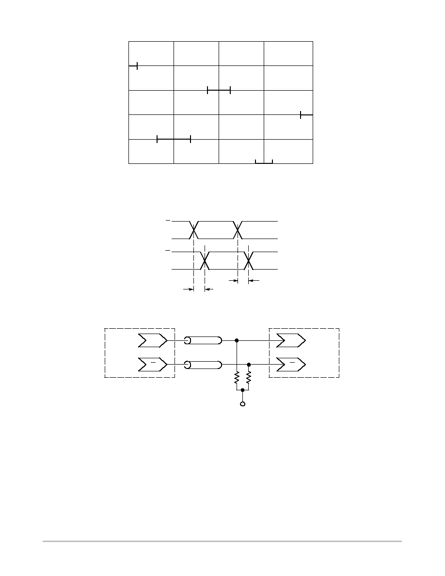
Figure 8. Eye Diagram at 3.2 Gb/s
(V
CC
- V
EE
= 3.3 V, OLS = FLOAT @ 25
5
C with input pattern of 2
31-1
PRBS, 5000 Waveforms)
X = 60 ps/div
Device Jitter = 6.8 ps
Total System Jitter = 17.2 ps
Input Generator Jitter = 10 ps
Y
= 75 mv/div
Figure 9. Eye Diagram at 7 GBit/s
(V
CC
- V
EE
= 3.3 V, OLS = FLOAT @ 25
5
C with input pattern of 2
31-1
PRBS, 5000 Waveforms)
X = 21 ps/div
Total System Jitter = 17.2 ps
Input Generator Jitter = 10 ps
Device Jitter = 7.2 ps
Y
= 80 mV/div
I
OLS
(
m
A)
-700
-600
-500
-400
-300
-200
-100
0
100
200
300
Figure 10. Typical OLS Input Current vs. OLS Input Voltage
(V
CC
- V
EE
= 3.3 V @ 25
5
C)
V
OLS
(mV)
V
EE
V
CC
V
CC
- 400
V
CC
- 800
V
CC
- 1200
NBSG72A
http://onsemi.com
12
V
OUTPP
(mV)
0
200
400
600
800
1000
OLS (mV)
Figure 11. OLS Operating Area
V
EE
V
CC
V
CC
- 400
V
CC
- 800
V
CC
- 1200
V
CC
- 75
V
CC
- 250
V
CC
- 550
V
CC
- 700
V
CC
- 900
V
CC
- 1125
V
CC
- 1275
V
EE
+ 100
Figure 12. AC Reference Measurement
D
D
Q
Q
t
PHL
t
PLH
V
INPP
= V
IH
(D) - V
IL
(D)
V
OUTPP
= V
OH
(Q) - V
OL
(Q)
Figure 13. Typical Termination for Output Driver and Device Evaluation
(See Application Note AND8020/D - Termination of ECL Logic Devices.)
Driver
Device
Receiver
Device
Q
D
Q
D
Z
o
= 50
W
Z
o
= 50
W
50
W
50
W
V
TT
V
TT
= V
CC
- 2.0 V
NBSG72A
http://onsemi.com
13
ORDERING INFORMATION
Device
Package
Shipping
NBSG72AMN
QFN-16
123 Units / Rail
NBSG72AMNG
QFN-16
(Pb-Free)
123 Units / Rail
NBSG72AMNR2
QFN-16
3000 / Tape & Reel
Board
Description
NBSG72AMNEVB
NBSG72AMN Evaluation Board
For information on tape and reel specifications, including part orientation and tape sizes, please refer to our Tape and Reel Packaging
Specifications Brochure, BRD8011/D.

NBSG72A
http://onsemi.com
14
Resource Reference of Application Notes
AN1405/D
- ECL Clock Distribution Techniques
AN1406/D
- Designing with PECL (ECL at +5.0 V)
AN1503/D
- ECLinPS
t
I/O SPiCE Modeling Kit
AN1504/D
- Metastability and the ECLinPS Family
AN1568/D
- Interfacing Between LVDS and ECL
AN1642/D
- The ECL Translator Guide
AND8001/D
- Odd Number Counters Design
AND8002/D
- Marking and Date Codes
AND8020/D
- Termination of ECL Logic Devices
AND8066/D
- Interfacing with ECLinPS
AND8090/D
- AC Characteristics of ECL Devices
NBSG72A
http://onsemi.com
15
PACKAGE DIMENSIONS
16 PIN QFN
MN SUFFIX
CASE 485G-01
ISSUE B
16X
SEATING
PLANE
L
D
E
0.15 C
A
A1
e
D2
E2
b
1
4
5
8
12
9
16
13
NOTES:
1. DIMENSIONING AND TOLERANCING PER
ASME Y14.5M, 1994.
2. CONTROLLING DIMENSION: MILLIMETERS.
3. DIMENSION b APPLIES TO PLATED
TERMINAL AND IS MEASURED BETWEEN
0.25 AND 0.30 MM FROM TERMINAL.
4. COPLANARITY APPLIES TO THE EXPOSED
PAD AS WELL AS THE TERMINALS.
5. L
max
CONDITION CAN NOT VIOLATE 0.2 MM
MINIMUM SPACING BETWEEN LEAD TIP
AND FLAG
«««
«««
«««
B
A
0.15 C
TOP VIEW
SIDE VIEW
BOTTOM VIEW
PIN 1
LOCATION
0.10 C
0.08 C
(A3)
C
16 X
e
16X
NOTE 5
0.10 C
0.05 C
A B
NOTE 3
K
16X
DIM
MIN
MAX
MILLIMETERS
A
0.80
1.00
A1
0.00
0.05
A3
0.20 REF
b
0.18
0.30
D
3.00 BSC
D2
1.65
1.85
E
3.00 BSC
E2
1.65
1.85
e
0.50 BSC
K
0.20
---
L
0.30
0.50
EXPOSED PAD
mm
inches
SCALE 10:1
0.50
0.02
0.575
0.022
1.50
0.059
3.25
0.128
0.30
0.012
3.25
0.128
0.30
0.012
EXPOSED PAD
*For additional information on our Pb-Free strategy and soldering
details, please download the ON Semiconductor Soldering and
Mounting Techniques Reference Manual, SOLDERRM/D.
SOLDERING FOOTPRINT*
NBSG72A
http://onsemi.com
16
ON Semiconductor and are registered trademarks of Semiconductor Components Industries, LLC (SCILLC). SCILLC reserves the right to make changes without further notice
to any products herein. SCILLC makes no warranty, representation or guarantee regarding the suitability of its products for any particular purpose, nor does SCILLC assume any liability
arising out of the application or use of any product or circuit, and specifically disclaims any and all liability, including without limitation special, consequential or incidental damages.
"Typical" parameters which may be provided in SCILLC data sheets and/or specifications can and do vary in different applications and actual performance may vary over time. All
operating parameters, including "Typicals" must be validated for each customer application by customer's technical experts. SCILLC does not convey any license under its patent rights
nor the rights of others. SCILLC products are not designed, intended, or authorized for use as components in systems intended for surgical implant into the body, or other applications
intended to support or sustain life, or for any other application in which the failure of the SCILLC product could create a situation where personal injury or death may occur. Should
Buyer purchase or use SCILLC products for any such unintended or unauthorized application, Buyer shall indemnify and hold SCILLC and its officers, employees, subsidiaries, affiliates,
and distributors harmless against all claims, costs, damages, and expenses, and reasonable attorney fees arising out of, directly or indirectly, any claim of personal injury or death
associated with such unintended or unauthorized use, even if such claim alleges that SCILLC was negligent regarding the design or manufacture of the part. SCILLC is an Equal
Opportunity/Affirmative Action Employer. This literature is subject to all applicable copyright laws and is not for resale in any manner.
PUBLICATION ORDERING INFORMATION
N. American Technical Support: 800-282-9855 Toll Free
USA/Canada
Japan: ON Semiconductor, Japan Customer Focus Center
2-9-1 Kamimeguro, Meguro-ku, Tokyo, Japan 153-0051
Phone: 81-3-5773-3850
NBSG72A/D
GigaComm is a trademark of Semiconductor Components Industries, LLC.
LITERATURE FULFILLMENT:
Literature Distribution Center for ON Semiconductor
P.O. Box 61312, Phoenix, Arizona 85082-1312 USA
Phone: 480-829-7710 or 800-344-3860 Toll Free USA/Canada
Fax: 480-829-7709 or 800-344-3867 Toll Free USA/Canada
Email: orderlit@onsemi.com
ON Semiconductor Website: http://onsemi.com
Order Literature: http://www.onsemi.com/litorder
For additional information, please contact your
local Sales Representative.