 | –≠–ª–µ–∫—Ç—Ä–æ–Ω–Ω—ã–π –∫–æ–º–ø–æ–Ω–µ–Ω—Ç: NCN6000 | –°–∫–∞—á–∞—Ç—å:  PDF PDF  ZIP ZIP |
©
Semiconductor Components Industries, LLC, 2002
October, 2002 ≠ Rev. 3
1
Publication Order Number:
NCN6000/D
NCN6000
Compact Smart Card
Interface IC
The NCN6000 is an integrated circuit dedicated to the smart card
interface applications. The device handles any type of smart card
through a simple and flexible microcontroller interface. On top of that,
due to the built≠in chip select pin, several couplers can be connected in
parallel. The device is particularly suited for low cost, low power
applications, with high extended battery life coming from extremely
low quiescent current.
Features
∑
100% Compatible with ISO7816≠3 and EMV Standard
∑
Wide Battery Supply Voltage Range: 2.7
v Vbat v 6.0 V
∑
Programmable CRD_VCC Supply to Cope with either 3.0 V or 5.0 V
Card Operation
∑
Built≠in DC/DC Converter Generates the CRD_VCC Supply with a
Single External Low Cost Inductor only, providing a High Efficiency
Power Conversion
∑
Full Control of the Power Up/Down Sequence Yields High Signal
Integrity on both the Card I/O and the Signal Lines
∑
Programmable Card Clock Generator
∑
Built≠in Chip Select Logic allows Parallel Coupling Operation
∑
ESD Protection on Card Pins (8.0 kV, Human Body Model)
∑
Fault Monitoring includes Vbat
low
and Vcc
low,
providing Logic
Feedback to External CPU
∑
Card Detection Programmable to Handle Positive or Negative Going
Input
∑
Built≠in Programmable CRD_CLK Stop Function Handles both High
or Low State
Typical Application
∑
E≠Commerce Interface
∑
ATM Smart Card
∑
Pay TV System
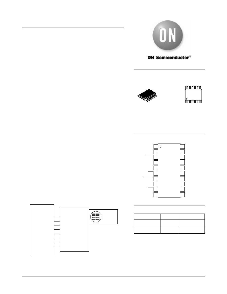
Figure 1. Simplified Application
MICRO
CONTROLLER
NCN6000
SMART CARD
INTERFACE
ISO/EMV
http://onsemi.com
Device
Package
Shipping
ORDERING INFORMATION
NCN6000DTB
TSSOP≠20
75 Units/Rail
TSSOP≠20
DTB SUFFIX
CASE 948E
1
20
MARKING
DIAGRAM
A
= Assembly Location
L
= Wafer Lot
Y
= Year
W
= Work Week
PIN CONNECTIONS
1
2
3
4
5
6
7
8
20
19
18
16
15
14
13
(Top View
)
STATUS
A0
A1
PGM
PWR_ON
CS
RESET
I/O
V
bat
L
out_
H
GROUND
CRD_V
CC
CRD_CLK
L
out_
L
CRD_IO
NCN
6000
ALYW
1
20
9
10
11
12
17
INT
CLOCK_IN
PWR_GND
CRD_RST
CRD_DET
NCN6000DTBR2
TSSOP≠20
2500/Tape & Reel
NCN6000
http://onsemi.com
2
GND
V
CC
PB7
PB6
PB5
PB4
PB3
PB2
PB1
PB0
IRQ
XTAL
MCU
GND
L1
1
2
3
4
5
6
7
8
9
10
20
19
18
17
16
15
14
13
12
11
A0
A1
PGM
PWR_ON
STATUS
CS
RESET
I/O
INT
CLOCK_IN
V
bat
L
out_H
L
out_L
PWR_GND
GROUND
CRD_V
CC
CRD_IO
CRD_CLK
CRD_RST
CRD_DET
22
µ
H
C3
C1
10
µ
F
100 nF
Swa
Swb
C8
C4
CLK
RST
V
CC
GND
I/O
17
18
8
4
3
2
1
5
7
VPP
SMARTCARD
J1
ISO7816
GND
GND
GND
GND
GND
GND
NCN6000
+5 V
10
µ
F
C2
U1
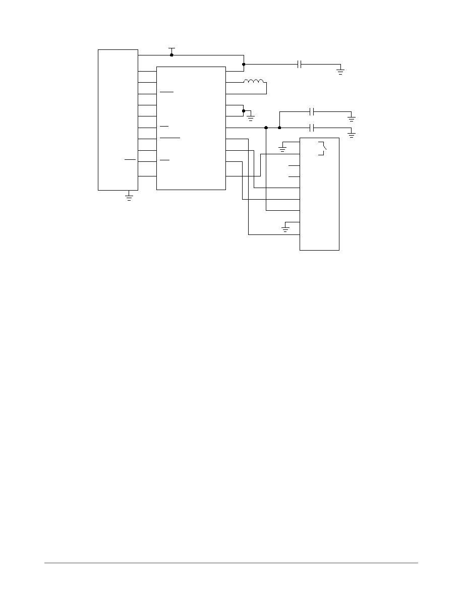
Figure 2. Typical Application
NCN6000
http://onsemi.com
3
GROUND
3
9
6
2
1
10
5
8
7
15
20
11
19
18
17
16
12
-
+
A0
A1
PGM
PWR_ON
STATUS
CS
RESET
I/O
INT
CLOCK_IN
V
bat
L
out_H
L
out_L
PWR_GND
CRD_V
CC
CRD_DET
S
R
Q
50
µ
s
Delay
CARD DETECTION
DECODER
1:16
CLOCK
DIVIDER
4
CARD STATUS
LOGIC & CARD PINS SEQUENCER
DC/DC STATUS
FAULT
ON/OFF
DC/DC CONVERTER
3 V / 5 V
A
STATUS INT
CLOCK
+V
bat
Power Down
Active Pwr_Down
V
bat
CLK STOP
ENABLE V
CC
STATUS INT
GND
V
bat
GND
CLOCK
CLK_STOP
SEQ 1
SEQ 2
SEQ 3
CRD_CLK
CRD_RST
CLOCK
13
I/O
I/O
14
CRD_IO
RESET
PWR_ON
V
bat
V
bat
V
bat
1
2
3
DATA
DATA
20 k
20 k
50 k
SEQ 1
SEQ 2
SEQ 3
2.0 V
GND
GND
500 k
+V
bat
50 k
GND
1/1
1/2
1/4
1/8
F
out
Set_V
CC
DATA
SELECT
V
bat_OK
V
CC
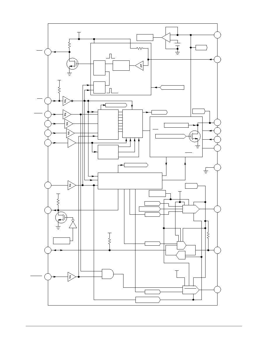
Figure 3. Block Diagram
V
CC
50 k
1
2
POLARITY
PROGRAMMABLE
V
bat_OK
V
bat_OK
NCN6000
http://onsemi.com
4
5 V CLOCK_IN 1/1
3 V CLOCK_IN 1/1
CS
I/O
A0
A1
RESET
PGM
STATUS
Program Chip
DC/DC OVERLOADED
CARD PRESENT NO CARD
Normal Chip Operation
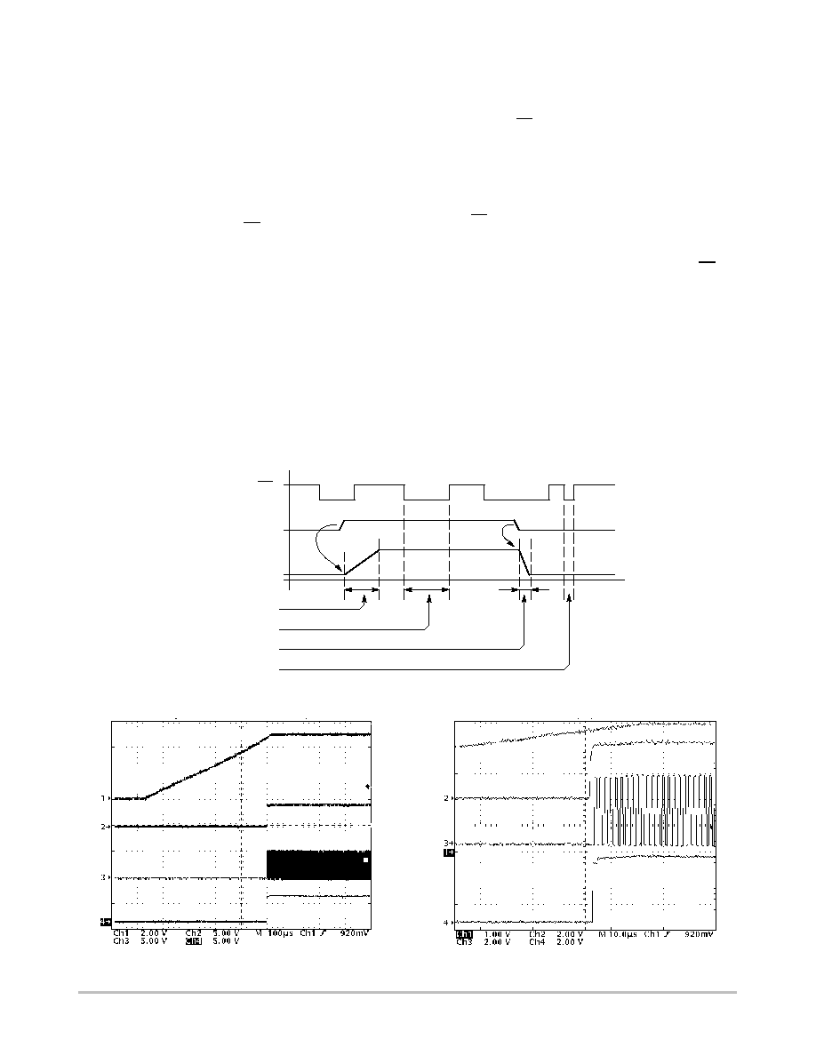
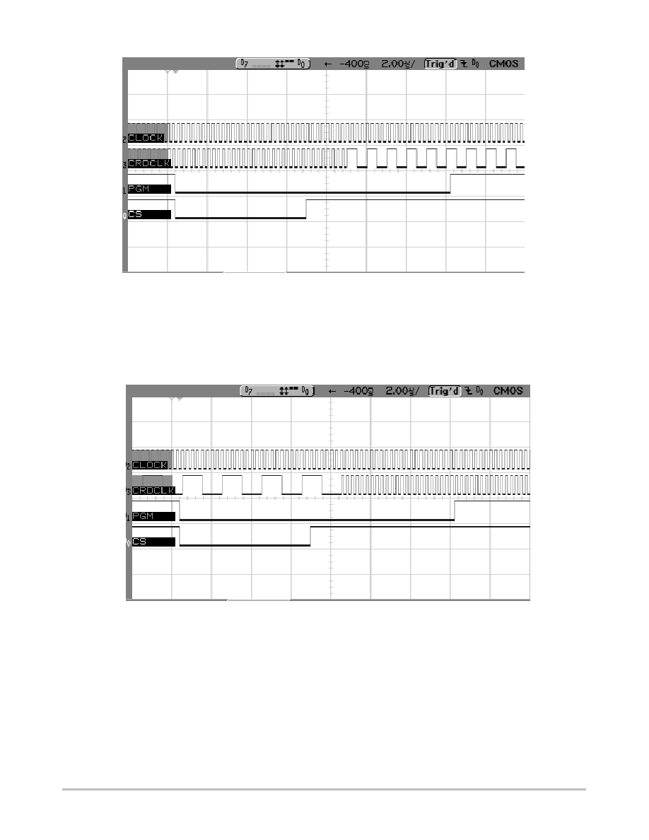
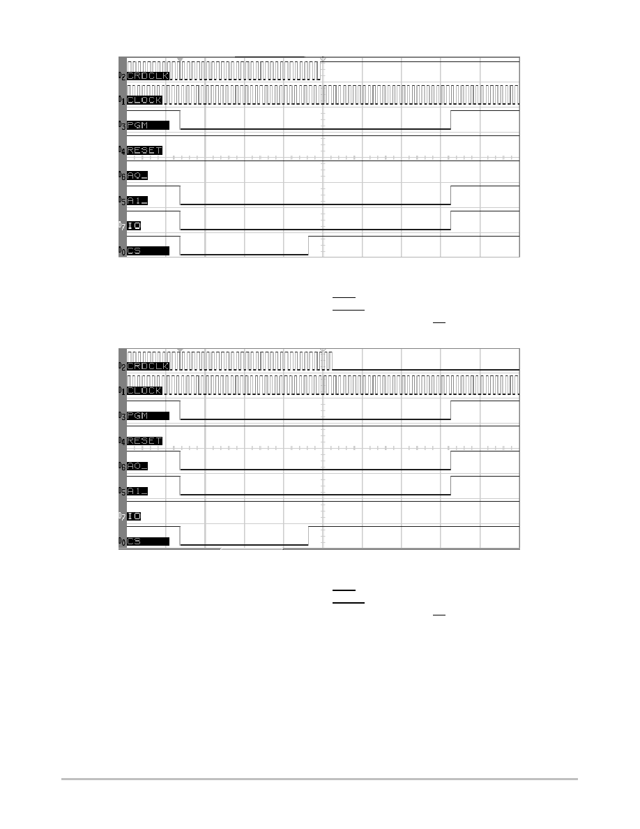
Figure 4. Programming and Normal Operation Basic Timing
DC/DC OK
3 V CLOCK_IN 1/2
3 V CLOCK_IN 1/4
3 V CLOCK_IN 1/8
5 V CLOCK_IN 1/2
5 V CLOCK_IN 1/4
5 V CLOCK_IN 1/8
ENABLE CRD_CLK
STOP CRD_CLKLow
STOP CRD_CLKHigh
Reserved
CRD_DET = Normally Open
CRD_DET = Normally Close
CRD_DET = Normally Close
CRD_DET = Normally Close
Read STATUS = 1≠> Card Present/ = 0≠> No Card
Read STATUS = 1≠>DC/DCOK/ = 0≠> DC/DC Overloaded
Read Vbat status≠> Low = Battery OK
Read CRD_V
CC
status≠> Low = CRD_V
CC
Low Voltage
1
2
3
4
5
6
7
8
9
0
1
2
3
4
5
6
7
8
9
0
STATUS
≠
≠
≠
≠
≠
≠
≠
≠
≠
≠
≠
≠
≠
≠
≠
≠
H/L
H/L
L/H
H/L
PGM
L
L
L
L
L
L
L
L
L
L
L
L
L
L
L
L
H
H
H
H
RESET
L
L
L
L
L
L
L
L
H
H
H
H
H
H
H
H
Z
Z
Z
Z
A1
L
L
L
L
H
H
H
H
L
L
L
L
H
H
H
H
L
L
H
H
A0
L
L
H
H
L
L
H
H
L
L
H
H
L
L
H
H
L
H
L
H
I/O
L
H
L
H
L
H
L
H
L
H
L
H
L
H
L
H
Z
Z
Z
Z
NCN6000
http://onsemi.com
5
The programming can be achieved with the card powered
ON or OFF. The identification of the interrupt is carried out
by polling the STATUS pin, the Vbat voltage and the DC/DC
results being provided on the same pin as depicted by the
table in Figure 4. During the programming mode, the PGM
pin can be released to High since the mode is internally
latched by the Negative going transition presents on the Chip
Select pin.
PGM
INT
CRD_DET
CARD EXTRACTED
CARD IDENTIFICATION
POLLING
50
µ
s
INTERRUPT
ACKNOWLEDGE
50
µ
s
High
Low
Low
CS
A0
A1
STATUS
S1 CLEAR INTERRUPT
S2 CARD PRESENT: STATUS = 1
S3 CLEAR INTERRUPT
S4 CARD PRESENT: STATUS = 0
Figure 5. Interrupt Servicing and Card Polling
When a card is either inserted or extracted, the CRD_DET
pin signal is debounced internally prior to pull the INT pin
to Low. The built≠in logic circuit automatically
accommodates positive or negative input signal slope, on
both insertion and extraction state, depending upon the
polarity defined during the initialization sequence. The
default condition is Normally Open switch, negative going
card detection. The external CPU shall acknowledge the
request by forcing CS = L which, in turn, releases the INT
pin to High upon positive going of Chip Select (Table 4).
Polling the STATUS pin as depicted in Table 3 identifies the
active card. If a card is present, the STATUS returns High,
otherwise a Low is presented pin 5. The 50
µ
s digital filter
is activated during both Insertion and Extraction of the card.
The MPU shall clear the INT line when the card has been
extracted, making the interrupt function available for other
purposes. However, neither the NCN6000 operation nor the
smart card I/O line or commands are affected by the state of
the INT pin.
On the other hand, clearing the INT and reading the
STATUS register can be performed by a single read by the
MPU: states S1 and S2 can be combined in a single
instruction, the same for S3 and S4.
NCN6000
http://onsemi.com
6
ABBREVIATIONS
Lout_H
DC/DC External Inductor
Lout_L
DC/DC External Inductor
Cout
Output Capacitor
VCC
Card Power Supply Input
Icc
Current at CRD_VCC Pin
Class A
5.0 V Smart Card
Class B
3.0 V Smart Card
CS
Chip Select (from MPU)
Z
High Impedance Logic State
(according to ISO7816)
CRD_VCC
Interface IC Card Power Supply Output
CRD_CLK
Interface IC Card Clock Output
CRD_RST
Interface IC Card Reset Output
CRD_IO
Interface IC Card I/O Signal Line
CRD_DET
Interface IC Card Detection
ATR
Answer to Reset
PGM
Select Programming or Normal Operation
INT
Interrupt (to MPU)
tr
Rise Time
tf
Fall Time
td
Delay Time
ts
Storage Time
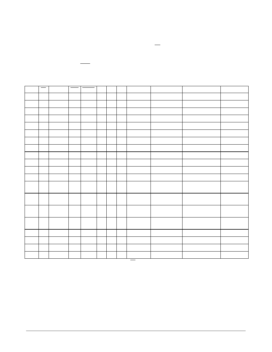
PIN FUNCTIONS AND DESCRIPTION
Pin
Name
Type
Description
1
A0
INPUT
This pin is combined with A1, PGM, RESET and I/O to program the chip mode of
operation and to read the data provided by STATUS.
(Figures 4 and 5 and Tables 2 and 3)
2
A1
INPUT
This pin is combined with A0, PGM, RESET and I/O to program the chip mode of
operation and to read the data provided by STATUS.
(Figures 4 and 5 and Tables 2 and 3)
3
PGM
INPUT
This pin is combined with A0, A1, RESET and I/O to program the chip mode of
operation and to read the data provided by STATUS.
(Figures 4 and 5 and Tables 2 and 3)
4
PWR_ON
INPUT
Pull Down
This pin validates the operation of the internal DC/DC converter:
CS = L + PWR_ON = Negative going: DC/DC is OFF
CS = L + PWR_ON = Positive going: DC/DC is ON
Note: The PWR_ON bit must be combined with a Low state CS signal to activate
the function. (Table 2)
5
STATUS
OUTPUT
This pin provides logic state related to the card and NCN6000 status. According to
the A0, A1 and PGM logic state, this pin carries either the Card present status or the
Vbat or the DC/DC operation state. When PGM = L, STATUS is not affected, see
Table 2.
6
CS
INPUT
Pull Up
This pin provides the NCN6000 chip select function. The PWR_ON, RESET, I/O, A0,
A1 and PGM signals are disabled when CS = H. When PGM = L and CS = L, the
device jumps to the programming mode (Figure 4 and Tables 1, 2 and 3). The Chip
Select pin must be a unique physical address when more than one card are
controlled by a single MPU. The data presented by the MPU are latched upon
positive going edge of the Chip Select pin.
NCN6000
http://onsemi.com
7
PIN FUNCTIONS AND DESCRIPTION (continued)
Pin
Description
Type
Name
7
RESET
INPUT
Pull Down
This pin provides two modes of operation depending upon the logic state of PGM
pin 3:
PGM = 1: The signal present at this pin is translated to pin 12 (card reset
signal) when CS = L and PWR_ON = H. It is latched when CS = H.
PGM = 0: The signal present on this pin is used as a logic input to program the
internal functions (Figure 5 and Tables 2 and 3).
8
I/O
Input/Output
Pull Up
This pin is connected to an external microcontroller interface. A bidirectional level
translator adapts the serial I/O signal between the smart card and the
microcontroller. The level translator is enabled when CS = L. The signal present on
this pin is latched when CS = H. This pin is also used in programming mode
(Tables 1, 2 and 3, Figures 4 and 5).
9
INT
OUTPUT
Pull Down
This pin is activated LOW when a card has been inserted and detected by the
interface or when the NCN6000 reports Vbat or CRD_VCC status (See Table 6). The
signal is reset to a logic 1 on the rising edge of either CS or PWR_ON. The Collector
open mode makes possible the wired AND/OR external logic. When two or more
interfaces share the INT function with a single microcontroller, the software must poll
the STATUS pin to identify the origin of the interrupt (Figure 5).
10
CLOCK_IN
CLOCK INPUT
High Impedance
This pin can be connected to either the microcontroller master clock, or to any clock
signal, to drive the external smart cards. The signal is fed to internal clock selector
circuit and translated to the CRD_CLK pin at either the same frequency, or divided
by 2 or 4 or 8, depending upon the programming mode (Tables 1, 2 and 3).
Care must be observed, at PCB level, to minimize the pick≠up noise coming from
the CLOCK_IN line. It is recommended to put a shield, built with a 10 mil copper
track, around this line and terminated to the GND.
11
CRD_DET
INPUT
The signal coming from the external card connector is used to detect the presence of
the card. A built≠in pull up low current source makes this pin active LOW or HIGH,
assuming one side of the external switch is connected to ground. At Vbat start up,
the default condition is Normally Open switch, negative going insertion detection.
The Normally Closed switch, positive going insertion detection, can be defined by
programming the NCN6000 accordingly. In this case, the polarity must be set up
during the first cycles of the system initialization, otherwise an already inserted card
will not be detected by the chip.
12
CRD_RST
OUTPUT
This pin is connected to the RESET pin of the card connector. A level translator
adapts the RESET signal from the microcontroller to the external card. The output
current is internally limited to 15 mA. The CRD_RST is validated when PWR_ON =
H and PGM = H and hard wired to Ground when the card is deactivated.
13
CRD_CLK
OUTPUT
This pin is connected to the CLK pin of the card connector. The CRD_CLK signal
comes from the clock selector circuit output. Combining A0, A1, PGM and I/O, as
depicted in Table 3 and Figure 3, programs the clock selection. This signal can be
forced into a standby mode with CRD_CLK either High or Low, depending upon the
mode defined by the programming sequence (Tables 1, 2 and 3 and Figure 4).
Care must be observed, at PCB level, to minimize the pick≠up noise coming from
the CRD_CLK line. It is recommended to put a shield, built with a 10mil copper track,
around this line and terminated to the GND.
14
CRD_IO
I/O
This pin handles the connection to the serial I/O pin of the card connector. A
bidirectional level translator adapts the serial I/O signal between the card and the
microcontroller. The CRD_IO pin current is internally limited to 15 mA. A built≠in
register holds the previous state presents on the I/O input pin.
15
CRD_VCC
POWER
This pin provides the power to the external card. It is the logic level "1" for CRD_IO,
CRD_RST and CRD_CLK signals. The energy stored by the DC/DC external
inductor Lout must be smoothed by a 10
µ
F capacitor, associated with a 100 nF
ceramic in parallel, connected across CRD_VCC and GND. In the event of a
CRD_VCC U
VLOW
voltage, the NCN6000 detects the situation and feedback the
information in the STATUS bit. The device does not take any further action,
particularly the DC/DC converter is neither stopped nor reprogrammed by the
NCN6000. It is up to the external MPU to handle the situation. However, when the
CRD_VCC is overloaded, the NCN6000 shut off the DC/DC converter, pulls the INT
pin Low and reports the fault in the STATUS register.
NCN6000
http://onsemi.com
8
PIN FUNCTIONS AND DESCRIPTION (continued)
Pin
Description
Type
Name
16
GROUND
SIGNAL
The logic and low level analog signals shall be connected to this ground pin. This pin
must be externally connected to the PWR_GND pin 17. The designer must make
sure no high current transients are shared with the low signal currents flowing into
this pin.
17
PWR_GND
POWER
This pin is the Power Ground associated with the built≠in DC/DC converter and must
be connected to the system ground together with GROUND pin 11. Using good
quality ground plane is recommended to avoid spikes on the logic signal lines.
18
Lout_L
POWER
The High Side of the external inductor is connected between this pin and Lout_H to
provide the DC/DC function. The built≠in MOS devices provide the switching function
together with the CRD_VCC voltage rectification.
19
Lout_H
POWER
The High Side of the external inductor is connected between this pin and Lout_L to
provide the DC/DC function. The current flowing into this inductor is limited by a
sense resistor internally connected from Vbat/pin 20 and pin 19. Typically, Lout =
22
m
H, with ESR < 2.0
W
, for a nominal 55 mA output load.
20
Vbat
POWER
This pin is connected to the supply voltage and monitored by the NCN6000. The
operation is inhibited when Vbat is below the minimum 2.70 V value, followed by a
PWR_DOWN sequence and a Low STATUS state.
MAXIMUM RATINGS
(Note 1)
Rating
Symbol
Value
Unit
Battery Supply Voltage
Vbat
7.0
V
Battery Supply Current (Note 2)
Ibat
300
mA
Power Supply Voltage
Vcc
6.0
V
Power Supply Current
Icc
"
100
mA
Digital Input Pins
Vin
≠0.5 V < V
in
< V
bat
+0.5 V,
but < 7.0 V
V
Digital Input Pins
Iin
"
5.0
mA
Digital Output Pins
Vout
≠0.5 V < V
in
< V
bat
+0.5 V,
but < 7.0 V
V
Digital Output Pins
Iout
"
10
mA
Card Interface Pins
Vcard
≠0.5 V < V
card
< CRD_VCC +0.5 V
V
Card Interface Pins, except CRD_CLK
Icard
"
15
mA
Inductor Current
ILout
300
mA
ESD Capability (Note 3)
Standard Pins
Card Interface Pins and CRD_DET
VESD
2.0
8.0
kV
TSSOP≠20 Package
Power Dissipation @ Tamb = +85
∞
C
Thermal Resistance Junction to Air (R
q
ja
)
P
DS
R
q
ja
320
125
mW
∞
C/W
Operating Ambient Temperature Range
TA
≠25 to +85
∞
C
Operating Junction Temperature Range
TJ
≠25 to +125
∞
C
Maximum Junction Temperature (Note 4)
TJmax
+150
∞
C
Storage Temperature Range
Tsg
≠65 to +150
∞
C
1. Maximum electrical ratings are defined as those values beyond which damage to the device may occur at T
A
= +25
∞
C.
2. This current represents the maximum peak current the pin can sustain, not the NCN6000 consumption (see Ibat
op
).
3. Human Body Model, R = 1500
, C = 100 pF.
4. Absolute Maximum Rating beyond which damage to the device may occur.
NCN6000
http://onsemi.com
9
POWER SUPPLY SECTION
(≠25
∞
C to +85
∞
C ambient temperature, unless otherwise noted.)
Rating
Symbol
Pin
Min
Typ
Max
Unit
Power Supply
Vbat
20
2.7
≠
6.0
V
Standby Supply Current Conditions:
PWR_ON = L, STATUS = H, CLOCK_IN = H,
CS = H. All other logic inputs and outputs are open:
Vbat = 3.0 V
Vbat = 5.0 V
Ibat
sb
20
≠
≠
3.0
≠
8.0
15
µ
A
DC Operating Current (Figure 19)
PWR_ON = H, CLOCK_IN = 0, CS = H, all CRD pins
unloaded
@ Vbat = 6.0 V, CRD_VCC = 5.0 V
@ Vbat = 3.6 V, CRD_VCC = 5.0 V
Ibat
op
20
≠
≠
7.0
2.0
≠
5.0
mA
Vbat Undervoltage Detection
High
Vbat Undervoltage Detection
Low
Vbat Undervoltage Detection
Hysteresis
Vbat
LH
Vbat
LL
Vbat
HY
20
2.1
2.0
≠
≠
≠
100
2.7
2.6
≠
V
V
mV
Output Card Supply Voltage @ Icc = 55 mA
@ 2.70 V
v
Vbat
v
6.0 V
CRD_VCC = 3.0 V
CRD_VCC = 5.0 V
@ Vbat
LL
< Vbat < 2.70 V
CRD_VCC = 5.0 V
Vcc
V
C3H
V
C5H
V
C5H
15
2.75
4.75
4.50
≠
≠
≠
3.25
5.25
≠
V
Output Card Supply Peak Current @ Vcc = 5.0 V
@ CRD_VCC = 5.0 V
@ CRD_VCC = 3.0 V
@ Vbat = 3.6 V, CRD_VCC = 5.0 V, Tamb < 65
∞
C
Iccp
15
55
55
65
≠
≠
≠
≠
≠
≠
mA
Output Current Limit Time Out
tdoff
15
≠
4.0
≠
ms
Output Over Current Limit
Iccov
15
≠
≠
100
mA
Output Dynamic Peak Current @ CRD_VCC = 3.0 V
or 5.0 V, Cout = 10
µ
F Ceramic XR7, Pulse Width
400 ns (Notes 5 and 6)
Iccd
15
100
≠
≠
mA
Battery Start≠Up Current
@ CRD_VCC = 3.0 V, ≠25
∞
C
v
TA
v
+ 85
∞
C
@ CRD_VCC = 5.0 V, ≠25
∞
C
v
TA
v
+ 85
∞
C
Icc
st
20
≠
≠
140
300
≠
≠
mA
Output Card Supply Voltage Ripple @ Lout = 22
µ
H,
Cout 1 = 10
µ
F, Cout 2 = 100 nF, Vbat = 3.6 V
Iout = 55 mA
CRD_VCC = 5.0 V
(Note 5)
CRD_VCC = 3.0V
Vcc
rip
15
≠
≠
≠
≠
50
50
mV
Output Card Supply Turn On Time @ Lout = 22
µ
F,
Cout1 = 10
µ
F, Cout2 = 100 nF, Vbat = 2.7 V,
CRD_VCC = 5.0 V
Vcc
TON
15
≠
≠
2.0
ms
Output Card Supply Shut Off Time @ Cout1 = 10
µ
F,
Ceramic, Vbat = 2.7 V, CRD_VCC = 5.0 V,
Vcc
OFF
< 0.4 V
Vcc
TOFF
15
≠
≠
250
µ
s
DC/DC Converter Operating Frequency
Fsw
18
≠
600
≠
kHz
Power Switch Drain/Source Resistor
R
ONS
18
≠
1.9
2.2
Output Rectifier ON Resistor
R
OND
15
≠
2.8
3.4
5. Ceramic X7R, SMD types capacitors are mandatory to achieve the CRD_VCC specifications. When electrolytic capacitor is used, the
external filter must include a 100 nF, max 50 m
ESR capacitor in parallel, to reduce both the high frequency noise and ripple to a minimum.
Depending upon the PCB layout, it might be necessary is to use two 6.8
µ
F/10 V/ceramic/X7R//SMD1206 in parallel, yielding an improved
CRD_VCC ripple over the temperature range.
6. According to ISO7816≠3, paragraph 4.3.2.
NCN6000
http://onsemi.com
10
DIGITAL PARAMETERS SECTION @ 2.70 V
v
Vbat
v
6.0 V, NORMAL OPERATING MODE
(≠25
∞
C to +85
∞
C ambient
temperature, unless otherwise noted.) Note: Digital inputs undershoot < ≠0.30 V to ground, Digital inputs overshoot <0.30 V to Vbat
Rating
Symbol
Pin
Min
Typ
Max
Unit
Input Asynchronous Clock Duty Cycle = 50%
@ Vbat = 3.0V over the temperature range
F
CLKIN
10
≠
≠
40
MHz
Clock Rise Time
Clock Fall Time
F
tr
F
tf
10
≠
≠
≠
≠
5.0
5.0
ns
I/O Data Transfer Switching Time,
Both Directions (I/O and CRD_IO),
@ Cout = 30 pF
I/O Rise Time* (Note 7)
I/O Fall Time
T
RIO
T
FIO
8, 14
≠
≠
0.8
0.8
µ
s
Input/Output Data Transfer Time, Both Directions
@ 50% CRD_VCC, L to H and H to L
T
TIO
8, 14
≠
≠
150
ns
Minimum PWR_ON Low Level Logic State Time
to Power Down the DC/DC Converter
T
WON
4
2.0
≠
≠
µ
s
CRD_VCC Power Up/Down Sequence Interval
T
DSEQ
≠
0.5
2.0
µ
s
STATUS Pull Up Resistance
R
STA
5
20
50
80
k
Chip Select CS Pull Up Resistance
R
CSPU
6
20
50
80
k
Interrupt INT Pull Up Resistance
R
INTPU
9
20
50
80
k
Positive Going Input High Voltage Threshold (A0,
A1, PGM, PWR_ON, CS, RESET, CRD_DET)
V
IH
1, 2,
3, 4,
6, 7,
11
0.70 * Vbat
≠
Vbat
V
Negative Going Input High Voltage Threshold
(A0, A1, PGM, PWR_ON, CS, RESET,
CRD_DET)
V
IL
1, 2,
3, 4,
6, 7,
11
0
≠
0.30 * Vbat
V
Output High Voltage
STATUS, INT @ I
OH
= ≠10
µ
A
V
OH
5, 9
Vbat ≠ 1.0 V
≠
≠
V
Output High Voltage
STATUS, INT @ I
OH
= 200
µ
A
V
OL
5, 9
≠
≠
0.40
V
7. Since a 20 k
pull up resistor is provided by the NCN6000, the external MPU can use an Open Drain connection.
DIGITAL PARAMETERS SECTION @ 2.70 V
v
Vbat
v
6.0 V, CHIP PROGRAMMING MODE
(≠25
∞
C to +85
∞
C ambient
temperature, unless otherwise noted.)
Rating
Symbol
Pin
Min
Typ
Max
Unit
A0, A1, PGM, PWR_ON, RESET and I/O
Data Set Up Time
T
SMOD
1, 2,
3, 4,
7, 8
2.0
≠
≠
µ
s
A0, A1, PGM, PWR_ON, RESET and I/O
Data Set Up Time
T
HMOD
1, 2,
3, 4,
7, 8
2.0
≠
≠
µ
s
Chip Select CS Low State Pulse Width
T
WCS
6
2.0
≠
≠
µ
s
NCN6000
http://onsemi.com
11
SMART CARD SECTION
(≠25
∞
C to +85
∞
C ambient temperature, unless otherwise noted.)
Rating
Symbol
Pin
Min
Typ
Max
Unit
CRD_RST @ CRD_VCC = +5.0 V
Output RESET V
OH
@ Icrd_rst = ≠20
µ
A
Output RESET V
OL
@ Icrd_rst = 200
µ
A
Output RESET Rise Time @ Cout = 30 pF
Output RESET Fall Time @ Cout = 30 pF
CRD_RST @ Vcc = +3.0 V
Output RESET V
OH
@ Icrd_rst = ≠20
µ
A
Output RESET V
OL
@ Icrd_rst = 200
µ
A
Output RESET Rise Time @ Cout = 30 pF
Output RESET Fall Time @ Cout = 30 pF
V
OH
V
OL
t
R
t
F
V
OH
V
OL
t
R
t
F
12
CRD_VCC ≠ 0.9
0
CRD_VCC ≠ 0.9
0
≠
CRD_VCC
0.4
100
100
CRD_VCC
0.4
100
100
V
V
ns
ns
V
V
ns
ns
CRD_CLK @ CRD_VCC = +3.0 V or +5.0 V
CRD_VCC = +5.0 V
Output Frequency (See Note 8)
Output Duty Cycle @ DC Fin = 50%
"
1%
Output CRD_CLK Rise Time @ Cout = 30 pF
Output CRD_CLK Fall Time @ Cout = 30 pF
Output V
OH
@ Icrd_clk = ≠20
µ
A
Output V
OL
@ Icrd_clk = 100
µ
A
CRD_VCC = +3.0 V
Output Frequency (See Note 8)
Output Duty Cycle @ DC Fin = 50%
"
1%
Output CRD_CLK Rise Time @ Cout = 30 pF
Output CRD_CLK Fall Time @ Cout = 30 pF
Output V
OH
@ Icrd_clk = ≠20
µ
A @ Cout = 30 pF
Output V
OL
@ Icrd_clk = 100
µ
A @ Cout = 30 pF
F
CRDCLK
F
CRDDC
t
R
t
F
V
OH
V
OL
F
CRDCLK
F
CRDDC
t
R
t
F
V
OH
V
OL
13
45
3.15
0
40
1.85
0
≠
5.0
55
18
18
CRD_VCC
+0.5
5.0
60
18
18
CRD_VCC
0.7
MHz
%
ns
ns
V
V
MHz
%
ns
ns
V
V
CRD_I/O @ CRD_VCC = +5.0 V
CRD_I/O Data Transfer Frequency
CRD_I/O Rise Time @ Cout = 30 pF
CRD_I/O Fall Time @ Cout = 30 pF
Output V
OH
@ Icrd_i/o = ≠20
µ
A
Output V
OL
@ Icrd_i/o = 500
µ
A, V
IL
= 0 V
CRD_I/O @ CRD_VCC = +3.0 V
CRD_I/O Data Transfer Frequency
CRD_I/O Rise Time @ Cout = 30 pF
CRD_I/O Fall Time @ Cout = 30 pF
Output V
OH
@ Icrd_i/o = ≠20
µ
A
Output V
OL
@ Icrd_i/o = 500
µ
A, V
IL
= 0 V
F
IO
T
RIO
T
FIO
V
OH
V
OL
F
IO
T
RIO
T
FIO
V
OH
V
OL
14
CRD_VCC ≠ 0.9
0
CRD_VCC ≠ 0.9
0
315
315
0.8
0.8
CRD_VCC
0.4
0.8
0.8
CRD_VCC
0.4
kHz
µ
s
µ
s
V
V
kHz
µ
s
µ
s
V
V
CRD_IO Pull Up Resistor @ PWR_ON = H
R
CRDPU
14
14
20
26
k
Card Detection Debouncing Delay:
Card Insertion
Card Extraction
T
CRDIN
T
CRDOFF
11
50
50
≠
150
150
µ
s
µ
s
Card Insertion or Extraction Positive Going Input
High Voltage
V
IHDET
11
0.70 * Vbat
≠
Vbat
V
Card Insertion or Extraction Negative Going Input
Low Voltage
V
ILDET
11
0
≠
0.30 * Vbat
V
Card Detection Bias Pull Up Current @
Vbat = 5.0 V
I
DET
11
≠
10
≠
µ
A
Output Peak Max Current Under Card Static
Operation Mode @ Vcc = 3.0 V or Vcc = 5.0 V
Icrd_iorst
12, 14
≠
≠
15
mA
Output Peak Max Current Under Card Static
Operation Mode @ Vcc = 3.0 V or Vcc = 5.0 V
Icrd_clk
13
≠
≠
70
mA
8. The CRD_CLK clock can operate up to 20 MHz, but the rise and fall time are not guaranteed to be fully within the ISO7816 specification over
the temperature range. Typically, tr and tf are 12 ns @ CRD_CLK = 10 MHz.
NCN6000
http://onsemi.com
12
Programming and Status Functions
The NCN6000 features a programming interface and a status interface. Figure
4
illustrates the programming mode.
Table 1. Programming and Status Functions Pinout Logic
Pins
Name
CRD_VCC
Prg. 3.0 V/5.0 V
CLOCK_IN
Divide Ratio
CRD_DET
CLOCK STOP
AND START
Poll Card
Status
DC/DC
Status
Vbat
Status
CRD_VCC
Status
5
STATUS
Not Affected
Not Affected
Not Affected
Not Affected
READ
READ
READ
READ
6
CS
Latch On
Rising Edge
Latch On
Rising Edge
Latch On
Rising Edge
Latch On
Rising Edge
0
0
0
0
3
PGM
0
0
0
0
1
1
1
1
1
A0
0/1
0/1
0/1
0/1
0
1
0
1
2
A1
0/1
0/1
1
0
0
0
1
1
7
RESET
0
0
1
1
Z
Z
Z
Z
8
I/O (in)
0/1
0/1
0/1
0/1
Z
Z
Z
Z
The PGM signal, pin 3, controls the mode of operation (chip programming or smart card transaction) and must be set up
accordingly prior to pull Chip Select (pin 6) Low.
Table 2. Status Pin Logic Output
Name
CS
PGM
A1
A0
Status Logic Level
None
H
X
X
X
No Chip Access
None
L
L
X
X
Programming Mode, No Read Available
CARD PRESENT
L
H
L
L
Low: No Card Inserted
High: Card inserted
DC/DC
L
H
L
H
Low: DC/DC Over Range
High: DC/DC Operates Normally
Vbat
L
H
H
L
Low: Vbat Within Range
High: Vbat Below Minimum range
CRD_VCC Overload
L
H
H
H
Low: CRD_VCC Voltage Below Minimum Range
High: CRD_VCC in Range
NCN6000
http://onsemi.com
13
Card VCC, Card CLOCK and Card Detection
Polarity Programming
The CRD_VCC and CLOCK_IN programming options
allows matching the system frequency with the card clock
frequency, and to select 3.0 V or 5.0 V CRD_VCC supply.
The CRD_DET programming option allows the usage of
either Normally Open or Normally Close detection switch.
Table 3 highlights the A0, A1, PGM and I/O logic states for
the possible options. The default power up reset condition
is state 1: asynchronous clock, ratio 1/1, CRD_CLK
active, CRD_DET = Normally Open, CRD_VCC = 3.0 V.
All states are latched for each output variable in
programming mode at the positive going slope of Chip
Select [CS] signal. It is the system designer's responsibility
to set up the options needed to match the chip with the
peripherals. In particular, when using Normally Close
switch, the CRD_DET polarity must be defined during the
first cycles of the initialization.
Table 3. Card VCC, Card Clock and Card Detection Polarity Truth Table
HEXA
CS
PWR_ON
PGM
RESET
A1
A0
I/O
CRD_VCC
CRD_CLK
CRD_DET
STATUS
$00
L
≠
L
L
L
L
L
3.0 V
CLOCK_IN 1/1
≠
H (Note 13)
$01
L
≠
L
L
L
L
H
3.0 V
CLOCK_IN 1/2
≠
H (Note 13)
$02
L
≠
L
L
L
H
L
3.0 V
CLOCK_IN 1/4
≠
H (Note 13)
$03
L
≠
L
L
L
H
H
3.0 V
CLOCK_IN 1/8
≠
H (Note 13)
$04
L
≠
L
L
H
L
L
5.0 V
CLOCK_IN 1/1
≠
H (Note 13)
$05
L
≠
L
L
H
L
H
5.0 V
CLOCK_IN 1/2
≠
H (Note 13)
$06
L
≠
L
L
H
H
L
5.0 V
CLOCK_IN 1/4
≠
H (Note 13)
$07
L
≠
L
L
H
H
H
5.0 V
CLOCK_IN 1/8
≠
H (Note 13)
$08
L
≠
L
H
L
L
L
≠
START
≠
H (Note 13)
$09
L
≠
L
H
L
L
H
≠
STOP Low
≠
H (Note 13)
$0A
L
≠
L
H
L
H
L
≠
STOP High
≠
H (Note 13)
$0B
L
≠
L
H
L
H
H
≠
Reserve
≠
H (Note 13)
$0C
L
≠
L
H
H
L
L
≠
≠
Normally Open
(Note 12)
H (Note 13)
$0D
L
≠
L
H
H
L
H
≠
≠
Normally Close
(Note 12)
H (Note 13)
$0E
L
≠
L
H
H
H
L
≠
≠
Normally Close
(Note 12)
H (Note 13)
$0F
L
≠
L
H
H
H
H
≠
≠
Normally Close
Note 12)
H (Note 13)
$10
L
≠
H
Z
L
L
Z
≠
≠
≠
Card Present
$12
L
1
H
Z
L
H
Z
≠
≠
≠
DC/DC status
$14
L
≠
H
Z
H
L
Z
≠
≠
≠
Vbat
$16
L
1
H
Z
H
H
Z
≠
≠
≠
CRD_VCC
9. The programmed conditions are latched upon the Chip Select (CS, pin 6) positive going transient.
10. Card clock integrity is guaranteed no spikes whatever be the frequency switching.
11. The STATUS register is not affected when the NCN6000 operates in any of the programming functions.
12. The CRD_VCC and CRD_CLK are not affected when the NCN6000 operates outside their respective decoded logic address.
13. The High Level on STATUS in registers $00 to $0F, inclusive, having being implemented to reduce current consumption but have no other
meanings.
14. At turn on, the NCN6000 is initialized with CRD_VCC = 3.0V, CLOCK_IN Ratio = 1/1, CRD_CLK = START, CRD_DET = Normally Open.
NCN6000
http://onsemi.com
14
DC/DC Converter and Card Detector Status
The NCN6000 status can be polled when CS = L. Please
consult Figures 4 and 5 for a description of input and output
signals. The status message is described in Table 4.
Note: in order to cope with a start up under low battery
condition, the Vbat OK message uses a negative logic as
depicted here below.
Table 4. Card and DC/DC Status Output
PGM
A1
A0
STATUS
Message
HIGH
L
L
LOW
No Card
HIGH
L
L
HIGH
Card Present
HIGH
L
H
LOW
DC/DC Converter
Overloaded
HIGH
L
H
HIGH
DC/DC Converter OK
HIGH
H
L
LOW
Vbat OK
HIGH
H
L
HIGH
Vbat Undervoltage
HIGH
H
H
HIGH
CRD_VCC OK
HIGH
H
H
LOW
CRD_VCC Undervoltage
The STATUS pin provides a feedback related to the
detection of the card, the state of the DC/DC converter, the
Vbat undervoltage and CRD_VCC undervoltage situations.
When PGM = H, the STATUS pin returns a High if a card is
detected present, a Low being asserted if there is no card
inserted. In any case, the external card is not automatically
powered up. When the external MPU asserts PWR_ON = H,
together with CS = L, the CRD_VCC supply is provided to
the card and the state of the DC/DC converter, the Vbat and
the CRD_VCC can be polled through the STATUS pin.
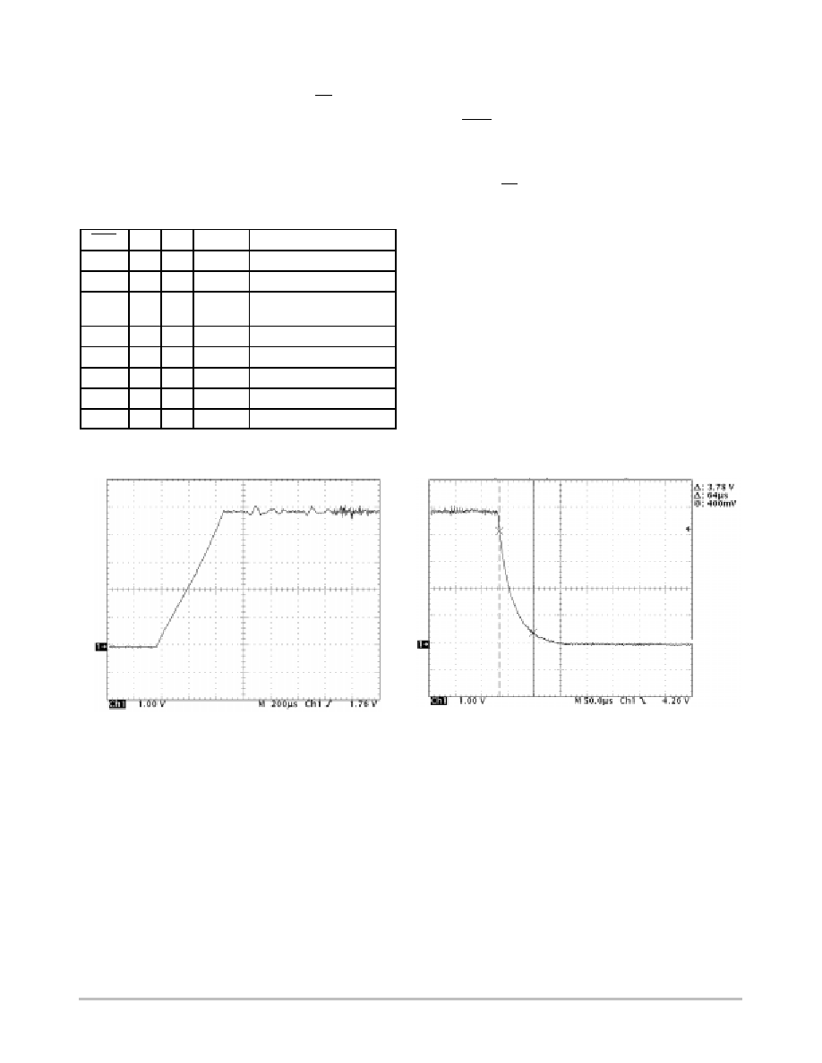
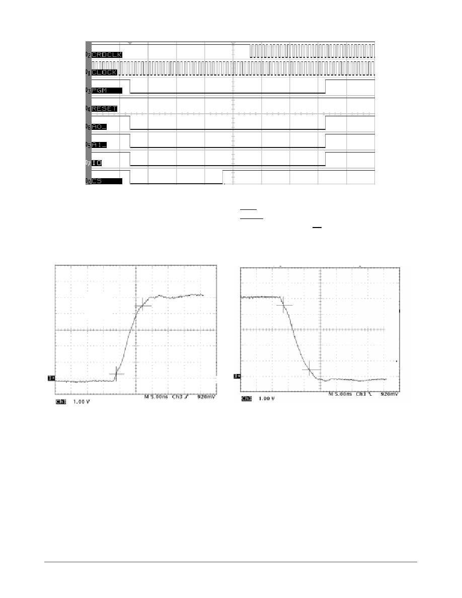
Card Power Supply Timing
At power up, the CRD_VCC power supply rise time
depends upon the current capability of the DC/DC converter
associated with the external inductor L1 and the reservoir
capacitor connected across CRD_VCC and GROUND.
On the other hand, at turn off, the CRD_VCC fall time
depends upon the external reservoir capacitor and the peak
current absorbed by the internal CMOS transistor built
across CRD_VCC and GROUND. These behaviors are
depicted in Figure 6. Since these parameters have finite
values, depending upon the external constraints, the
designer must take care of these limits if the t
ON
or the t
OFF
provided by the data sheets does not meet his requirements.
Figure 6. Card Power Supply Turn ON and OFF Timing
Typical CRD_VCC Rise Time @ Cout = 10
m
F, V = 5.0 V
Typical CRD_VCC Fall Time @ Cout = 10
m
F, V = 5.0 V

NCN6000
http://onsemi.com
15
Basic Operating Modes Flow Chart
The NCN6000 brings all the functions necessary to handle
data communication between a host computer and the smart
card. The built≠in Chip Select pin provides a simple way to
share the same MPU bus with several card interface. On top
of that, the logic control are derived from specific pins,
avoiding the risk of mixing up the operation when the
interface is controlled by a low end microcontroller.
During the transaction operation, the external MPU takes
care of whatever is necessary to he data on the single
bidirectional I/O line. Leaving aside the DC≠DC control and
associated failures, the NCN6000 does not take any further
responsibility in the data transaction.
When the chip operates in the programming mode, the
NCN6000 provide a flexible access to set up the CRD_VCC
voltage, the CRD_CLK and the CRD_DET smart card
signals.
The external microcontroller takes care of the smart card
transaction and shall handle the interface accordingly.
Figure 7. Operating Modes Flow Chart
RESET
Vbat = OK
STAND BY MODE
SELECT OPERATING MODE
PROGRAMMING
MODE
SET NCN6000
PARAMETERS
ACTIVE MODE
SEND ATR SEQUENCE
TRANSACTION MODE
END MODE
POWER DOWN SEQUENCE
IDLE MODE
FINISH
PWR_ON = H
CS = H
CS = H
PGM = H
PGM = L
CS = L
PGM = H
CS = L
LATCH NCN6000
PARAMETERS
PGM = H
CS = H
Standby Mode
The Standby Mode allows the NCN6000 to detect a card
insertion, keeping the power consumption at a minimum.
The power supply CRD_VCC is not applied to the card, until
the external controllers set PWR_ON = H with CS = L.
Standby Mode
Logic Conditions:
Card Output:
CS
= H
PWR_ON = H
A0
= Z
A1
= Z
PGM
= Z
I/O
= Z
RESET
= Z
CRD_VCC = 0 V
CRD_CLK = L
CRD_RST = L
CRD_IO
= L
When a card is inserted, the internal logic filters the signal
present pin 11, then asserts the INT pin to Low if the pulse
applied to CRD_DET is longer than 150
ms. The external
MPU shall run whatever is necessary to handle the card.
The INT is cleared (return to High) when a positive going
transition is asserted to either the CS or to the PWR_ON
signal logically combined with Chip Select = Low.

NCN6000
http://onsemi.com
16
Programming Mode
The programming mode allows the configuration of the
card power supply, card clock and Card Detection input
logic polarity. These signals (CRD_VCC, CRD_CLK and
CRD_DET) are described in the pin description paragraph
associated with Tables 1 and 3 and Figures 4 and 8.
Programming Mode
Logic Conditions:
Card Output:
CS
= L
PWR_ON = L
A0
= H/L
A1
= H/L
PGM
= L
I/O
= L/H
RESET
= L/H
CRD_VCC = 0 V
CRD_CLK = L
CRD_RST = L
CRD_IO
= H/L depending upon
the previous I/O pin
logic state
The I/O and RESET pins are not connected to the smart
card and become logic inputs to control the NCN6000
programming sequence. The programmed values are
latched
upon transition of CS from Low to High, PGM being
Low during the transition.
When a programming mode is validated by a Chip Select
negative going transient, the mode is latched and PGM can
be released to High. This latch is automatically reset when
CS returns to High.
The logic input signals can be set simultaneously, or one
bit a time (using either a STAA or a BSET function), the key
point being the minimum delay between the shorter bit and
the Chip Select pulse. The programmed value is latched into
the NCN6000 register on the CS positive going edge.
PROGRAMMING
2
µ
s
2
µ
s
1
µ
s
NORMAL MODE
PGM
I/O
A0
A1
RESET
CS
Figure 8. Minimum Programming Timings
Active Mode
In the active mode, the NCN6000 is selected by the
external MPU and the STATUS pin can be polled to get the
status of either the DC/DC converter or the presence of the
card (inserted or not valid). The power is not connected to
the card: CRD_VCC = 0 V.
Active Mode
Logic Conditions:
Card Output:
CS
= L
PWR_ON = L
A0
= L
A1
= L
PGM
= H
I/O
= Z
RESET
= Z
STATUS
= L/H is Card
Inserted?
CRD_VCC = 0 V
CRD_CLK = L
CRD_RST = L
CRD_IO
= H/L depending upon
the previous I/O pin
logic state
The Chip Select pulse [CS] will automatically clear the
previously asserted INT signal upon the positive going
transition.
If a card is present, the MPU shall activate the DC/DC
converter by asserting PWR_ON = H. The NCN6000 will
automatically run a power up sequence when the
CRD_VCC reaches the undervoltage level (either V
C5H
or
V
C3H
, depending upon the CRD_VCC voltage supply
programmed). The CRD_IO, CRD_RST and CRD_CLK
pins are validated, according to the ISO7816≠3 sequence.
The interface is now in transaction mode and the system is
ready for data exchange through the I/O and RESET lines.
At any time, the microcontroller can change the CRD_CLK
frequency and mode, or the CRD_VCC value as determined
by the card being in use.

NCN6000
http://onsemi.com
17
Transaction Mode
During the transaction mode, the NCN6000 maintains
power supply and clock signal to the card. All the signal
levels related with the card are translated as necessary to
cope with the MPU and the card.
The DC/DC converter status and the Vbat state can be
monitored on the STATUS by using the A0 and A1 logic
inputs as depicted in Tables 3 and 4.
Transaction Mode
Logic Conditions:
Card Output:
CS
= L
PWR_ON = H
A0
= H
A1
= H
PGM
= H
I/O
= DATA
TRANSFER
RESET
= H/L
STATUS
= L/H DC/DC
status: Fail/Pass?
CRD_VCC = 3.0 or 5.0 V
CRD_CLK = CLOCK
CRD_RST = H/L
CRD_IO
= DATA
TRANSFER
To make sure the data are not polluted by power losses, it
is recommended to check the state of CRD_VCC before
launching a new data transaction. Since CS = L, this is
achieved by forcing bits A0 and A1 according to Table 4, and
reading the STATUS pin 5.
Idle Mode
The idle mode is used when a card is powered up
(CRD_VCC = Vcc), without communication on going.
Idle Mode
Logic Conditions:
Card Output:
CS
= L
PWR_ON = H
A0
= H
A1
= H
PGM
= H
I/O
= Z
RESET
= H
STATUS
= L/H according
to the internal
register results
CRD_VCC = 3.0 or 5.0 V
CRD_CLK = CLOCK active or
L or H
CRD_RST = H
CRD_IO
= Z
In addition, the CRD_CLK signal can be stopped, as
depicted in Tables 3 and 4, to minimize the current
consumption of the external smart card, leaving CRD_VCC
active.
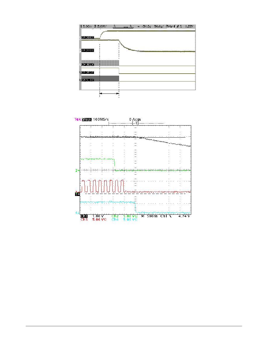
Power Down Operation
The power down mode can be initiated by either the
external MPU (pulling PWR_ON = L) or by one of the
internal error condition (CRD_VCC overload or Vbat Low).
The communication session is terminated immediately,
according to the ISO7816≠3 sequence. On the other hand,
the MPU can run the Standby mode by forced CS = H.
When the card is extracted, the interface shall detect the
operation and run the Power Shut Off of the card as
described by the ISO/CEI 7816≠3 sequence depicted here
after:
ISO7816≠3 sequence:
Force RST to Low
Force CLK to Low, unless it is already in this state
Force CRD_IO to Low
Shut Off the CRD_VCC supply
Since the internal digital filter is activated for any card
insertion or extraction, the physical power sequence will be
activated 150
ms maximum after the card has been extracted.
Of course, such a delay does not exist when the MPU launch
the power down intentionally.
The time delay between each negative going signal is
500 ns typical (Figure 10).
NCN6000
http://onsemi.com
18
CARD EXTRACTION
DETECTED
CRD_VCC
Voltage
CRD_CLK
CRD_RST
CRD_IO
Digital Filter Delay (50
µ
s min)
Figure 9. Typical Power Down Sequence in the NCN6000 Interface
Figure 10. Power Down Sequence Details
CRD_VCC
CRD_CLK
CRD_RST
CRD_IO
NCN6000
http://onsemi.com
19
Card Detection
The card detector circuit provides a 500 k
W pull up
resistor to bias the CRD_DET pin, yielding a logic High
when the pin is left open (assuming a NO switch). The
internal logic associated with pin 11 provides an automatic
selection of the slope card detection, depending upon the
polarity set by the external MPU. At start up, the CRD_DET
is preset to cope with Normally Open switch. When a
Normally Close switch is used in the card socket, it is
mandatory to program the NCN6000 chip during the
initialization sequence, otherwise the system will not start if
a card was previously inserted. Table 3 gives the
programming code for such a function. The next lines
provide a typical assembler source to handle this CRD_DET
Normally Close polarity:
Smart EQU $20
LDX
#$1000
LDAA #$09
STAA smart, X
; NCN6000 Physical CS Address
; Offset
; I/O = H, A0 = A1 = L, RESET = H
; Set CRD_DET = Normally Closed
Switch
The CRD_DET polarity can be updated at any time,
during the Program Mode sequence (PGM = L), but,
generally speaking, is useless since the switch does not
change during the usage of the considered module. On the
other hand, the card detection switch shall be connected
across pin 11 and ground, for any polarity selected.
The transition presents pin 11, whatever be the polarity, is
filtered out by the internal digital filter circuit, avoiding false
interrupt. In addition to the minimum internal 50
ms timing,
the MPU shall provide an additional delay to cope with the
mechanical stabilization of the card interface (typically
3 ms), prior to valid the CRD_VCC supply.
When a card is inserted, the detector circuit asserts
INT = Low as depicted before. When the NCN6000 detects
a card extraction, the power down sequence is activated,
regardless of the PWR_ON state, and the INT pin is asserted
Low. It is up to the external MPU to clear this interrupt by
forcing a chip select pulse as depicted in Figure 5.
The 75
ms delay represent the digital filter built≠in the
NCN6000 chip being used for the characterization. Any
pulse shorter than this delay does not generate an interrupt.
However, to guarantee an interrupt will be generated, the
CRD_DET signal must be longer than 150
ms as defined by
the specification.
The Chip Select pulse is generated by the external
microcontroller, the minimum pulse width being 2
ms to
make sure the card is detected.
The oscillogram, Figure 11, depicts the behavior for a
Normally Open switch, the delay existing between the
interrupt negative going state and the CS being Low comes
from the particular software latency existing in this
particular MPU.
Figure 11. Card Insertion Detection and Interrupt Signals
Digital Filter Delay
INTERRUPT
Chip Select Acknowledge or Clear Interrupt

NCN6000
http://onsemi.com
20
CRD_DET Input Voltage (card extracted)
Digital Filter Delay
INTERRUPT
Chip Select Acknowledge or Clear Interrupt
Figure 12. Card Extraction Detection and Interrupt Signals
When the card is extracted, the CRD_DET signal
generates an interrupt, assuming the positive pulse width is
longer than the digital filter. The oscillogram, Figure 12,
depicts the behavior for a Normally Open switch.
Note: since the internal pull up resistor is relatively high
(500 k
typical), one must use a 10 M
input impedance
probe to read this signal.
CRD_DET Input Voltage (card inserted)
INTERRUPT
Chip Select
Figure 13. Interrupt Acknowledgement During a Card Insertion Detection Sequence
The interrupt signal, provided pin 9, is cleared by a
positive going Chip Select signal as depicted by the
oscillogram, Figure 13. The CS pulse width is irrelevant, as
long as it is larger than 2.0
ms, to activate a different
sequence. Leaving the interrupt signal Low has no influence
on the internal behavior of the NCN6000, but will be
automatically cleared when the DC/DC will be activated by
the MPU (CS=L, PWR_ON = Positive High transition)
NCN6000
http://onsemi.com
21
Power Management
The purpose of the power management is to activate the
circuit functions needed to run a given mode of operation,
yielding a minimum current consumption on the Vbat
supply. In the Standby mode (PWR_ON = L), the power
management provides energy to the card detection circuit
only. All the card interface pins are forced to ground
potential.
In the event of a power up request coming from the
external MPU (PWR_ON = H, CS = L), the power manager
starts the DC/DC converter.
When the CRD_VCC voltage reaches the programmed
value (3.0 V or 5.0 V), the circuit activates the card signals
according to the following sequence:
CRD_VCC
CRD_IO
CRD_CLK
CRD_RST
The logic level of the data lines are asserted High or Low,
depending upon the state forced by the external MPU, when
the start up sequence is completed. Under no situation the
NCN6000 shall launch automatically a smart card ATR
sequence. Assuming PWR_ON = H, the CRD_VCC voltage
is maintained whatever be the logic level presents on Chip
Select, pin 6.
At the end of the transaction, asserted by the MPU
(PWR_ON = L, CS = L), or under a card extraction, the
ISO7816≠3 power down sequence takes place:
CRD_RST
CRD_CLK
CRD_IO
CRD_VCC
When CS = H, the bi≠directional I/O line (pins 8 and 15)
is forced into the High impedance mode to avoid signal
collision with any data coming from the external MPU.
The CRD_VCC voltage is controlled by means of CS and
PWR_ON logic signal as depicted in Figure 14. The
PWR_ON logic level define the CRD_VCC voltage status,
the amplitude being the one pre programmed into the chip.
In order to avoid uncontrolled command applied to the
smart card, the NCN6000 internal logic circuit, together
with the Vbat monitoring, clamps the card outputs until the
CRD_VCC voltage reaches the minimum value. During the
CRD_VCC slope, all the card outputs are kept Low and no
spikes can be write to the smart card. The oscillogram on the
right hand side is a magnification of the curves given on the
opposite side.
CS
PWR_ON
CRD_VCC
CRD_VCC
Rise Time
CRD_VCC
No Change
CRD_VCC
Power Down Fall Time
CRD_VCC No Change
250
µ
s
2 ms
Figure 14. Card Power Supply Control
Figure 15. Smart Card Signals Sequence at Power On
CRD_VCC
CRD_CLK
CP = 15 pF
CRD_RST
CRD_IO
5.0 V
CRD_VCC
CRD_CLK
CRD_RST
CRD_IO
5.0 V
CP = 15 pF
NCN6000
http://onsemi.com
22
Vbat Supply Voltage Monitoring
The built≠in comparator, associated with the band gap
reference, continuously monitors the +Vbat input. During
the start up, all the NCN6000 functions are deactivated and
no data transfer can take place. When the +Vbat voltage rises
above 2.35 V (typical), the chip is activated and all the
functions becomes available. The typical behavior is
provided here after Figure 16. At this point, the internal
Power On Reset signal is activated (not accessible
externally)
and all the logic signals are forced into the states
as defined by Table 3.
If the +Vbat voltage drops below 2.25 V (typical) during
the operation, the NCN6000 generate a Power Down
sequence and is forced in a no operation mode. The built≠in
100 mV (typical) hysteresis avoids unstable operation when
the battery voltage slowly varies around the 2.30 V.
On the other hand, the microcontroller can read the
STATUS signal, pin 5, to control the state of the battery prior
to launch either a NCN6000 programming or an ATR
sequence (Table 4).
2.80 V
Figure 16. Typical Vbat Monitoring
Vbat
2.35 V
2.25 V
3.30 V
Vbat_OK
Vbat STATUS
Note: Drawing is not to scale and voltages are typical.
See specifications data for details.
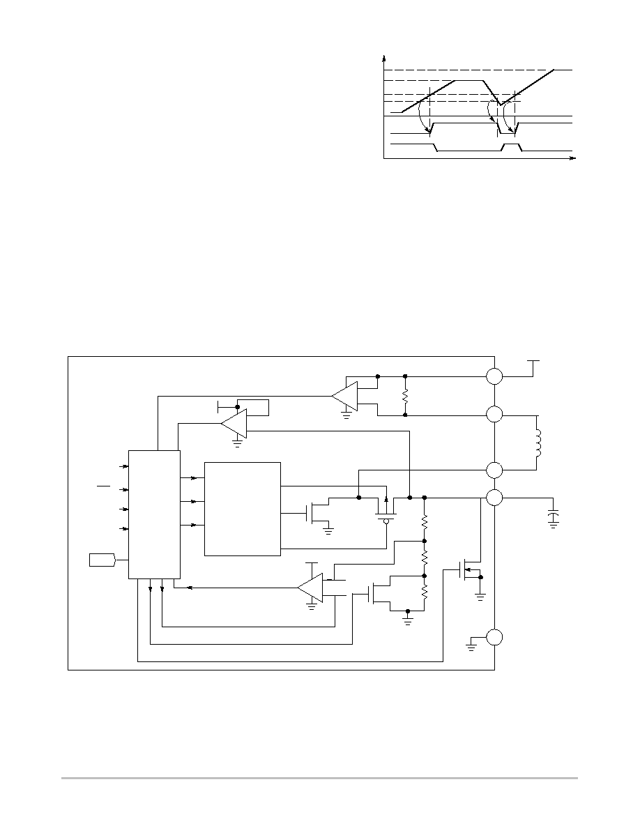
DC/DC Converter Operation
The built≠in DC/DC converter is based on a modified
boost structure to cover the full battery and card operating
voltage range. The built≠in battery voltage monitor provides
an automatic system to accommodate the mode of operation
whatever be the Vbat and CRD_VCC voltages. Comparator
U3/Figure 17 tracks the two voltages and set up the
operating mode accordingly.
U2
≠
+
U3
V
ref
-
+
MOS Drive
Substrat Bias
U1
PWR_ON
3 V/ 5 V
Overload
VCC_OK
R1
1R
Current Sense
20
19
18
15
17
V
bat
V
bat
L2
22
µ
H
L
out_L
L
out_H
+
GND
CRD_VCC
C1
GND
GND
GND
V
out
_3_5
V
ref
_3/5 V
Voltage Regulation
V
bat
Q3
Q1
Q2
GND
V
bat
V
bat
/V
CC
Comparator
NMOS Gate Drive
PMOS Gate Drive
LOGIC CONTROL
GND
PWR_GND
GND
Figure 17. Basic DC/DC Structure
≠
+
R2
R3
R4
Active Pull Down
GND
Q4
NCN6000
http://onsemi.com
23
When the input voltage Vbat is lower than the
programmed CRD_VCC, the system operates under the
boost mode, providing the voltage regulation and current
limit to the smart card. In this mode, the external inductor,
typically 22
mH, stores the energy to drive the +5.0 V card
supply from the external low voltage battery. The
oscillogram, Figure 18, depicts the DC/DC behavior under
these two modes of operation.
Beside the DC/DC converter, NMOS Q4 provides a low
impedance to ground during the Power Down sequence,
yielding the 250
ms maximum switch time depicted in the
data sheet.
Figure 18. DC/DC Operating Modes
Step Down Mode
CRD_VCC 5 V Step Up Mode
CRD_VCC
I
L
Ibat
DC Operating Current @ CRD_VCC = 5.0 V
0
1
2
3
4
5
6
7
8
2.5
3.0
3.5
4.0
4.5
5.0
5.5
6.0
Vbat (V)
Ibat_op (mA)
25
∞
C
85
∞
C
POWER_ON
Figure 19. Typical DC Operating Current
≠25
∞
C
When the input voltage Vbat is higher than the
programmed CRD_VCC, the system operates under a step
down mode, yielding the voltage regulation and current
limit identical to the boost mode. In this case, the built≠in
structure turns Off Q1 and inverts the Q2 substrate bias to
control the current flowing to the load.These operations are
fully automatic and transparent for the end user.
The High and Low limits of the current flowing into the
external inductor L1 are sensed by the operational amplifier
U1 associated with the internal shunt R1. Since this shunt
resistor is located on the hot side of the inductor, the device
reads both the charge and discharge of the inductor,
providing a clean operation of the converter.
In order to optimize the DC/DC power conversion
efficiency, it is recommended to use external inductor with
R < 2.0
.
The output capacitor C1 stores the energy coming from the
converter and smooths the CRD_VCC voltage applied to the
external card. At this point, care must be observed, beside the
micro farad value, to select the right type of capacitor.
According to the capacitor's manufacturers, the internal ESR
can range from a low 10 m
to more than 3.0
, thus yielding
high losses during the DC/DC operation, depending upon the
technology used to build the capacitor.
The standard electrolytic capacitors have the low cost
advantage for a relative high micro farad value, but have
poor tolerance, high leakage current and high ESR.
The tantalum type brings much lower leakage current
together with high capacity value per volume, but cost can
be an issue and ESR is rarely better than 500 m
.
The new ceramic type have a very low leakage together
with ESR in the 50 m
range, but value above 10
mF are
relatively rare. Moreover, depending upon the low cost
ceramic material used to build these capacitors, the thermal
coefficient can be very bad, as depicted in Figure 20. The
X7R type is highly recommended to achieve low voltage
ripple.
Figure 20. Typical Y7R Ceramic Type Value as a
Function of the Temperature.
100%
≠25
∞
C
+25
∞
C
+85
∞
C
15%
NCN6000
http://onsemi.com
24
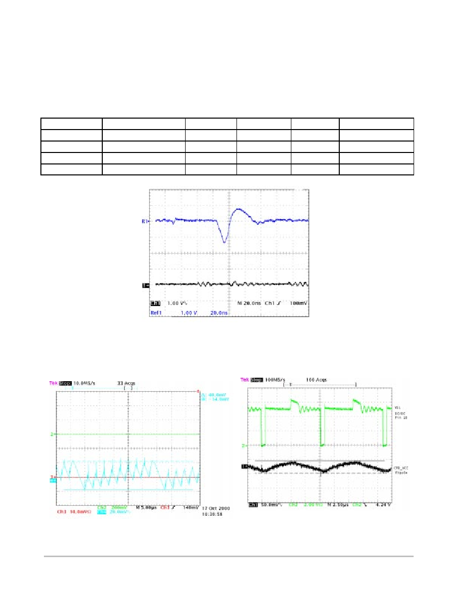
Based on the experiments carried out during the
NCN6000 characterization, the best comprise, at time of
printing this document, is to use two
6.8
mF/10 V/Ceramic/X7R capacitor in parallel to achieve
the CRD_VCC filtering. The ESR will not extend 50 m
over the temperature range and the combination of standard
parts provide an acceptable ≠20% to +20% tolerance,
together with a low cost. Obviously, the capacitor must be
SMD type to achieve the extremely low ESR and ESL
necessary for this application. Figure 21 illustrates the
CRD_VCC ripple observed in the NCN6000 demo board
depending upon the type of capacitor used to filter the output
voltage.
Table 5. Ceramic/Electrolytic Capacitors Comparison
Manufacturers
Type/Series
Format
Max Value
Tolerance
Typ. Z @ 500 kHz
MURATA
CERAMIC/GRM225
0805
10
m
F/6.3 V
+80%/≠20%
30 m
W
VISHAY
Tantalum/594C/593C
10
m
F/16 V
450 m
W
VISHAY
Electrolytic/94SV
10
m
F/10 V
≠20%/+20%
400 m
W
Electrolytic Low Cost
10
m
F/10 V
≠35%/+50%
2.0
W
Top Trace = Electrolytic or Tantalum 10
m
F
Bottom Trace = X7R 10
m
F ceramic
The high ripple pulse across CRD_VCC is the consequence
of the large ESR of the electrolytic capacitor.
Figure 21. CRD_VCC Ripple as a Function of the Capacitor Technology
C= 10
m
F
Electrolytic or Tantalum
C= 10
m
F
Ceramic
NOTES: Rload = 100
, Vbat = 5.0 V, CRD_VCC = 5.0 V
Cout = 10
m
F/X7R, CRD_CLK = Stop High
Figure 22. External Capacitor Current Charge and
CRD_VCC Voltage Ripple.
Figure 23. CRD_VCC Voltage Ripple

NCN6000
http://onsemi.com
25
Clock Divider
The main purpose of the built≠in clock generator is
threefold:
1. Adapts the voltage level shifter to cope with the
different voltages that might exist between the MPU
and the Smart Card.
2. Provides a frequency division to adapt the Smart
Card operating frequency from the external clock
source.
3. Controls the clock state according to the smart card
specification.
In addition, the NCN6000 adjusts the signal coming from
the microprocessor to get the Duty Cycle window as defined
by the ISO7816≠3 specification.
The logic input pins A0, A1, PGM, I/O and RESET fulfill
the programming functions when both PGM and CS are
Low. The clock input stage (CLOCK_IN) can handle a
40 MHz frequency maximum, the divider being capable to
provide a 1:8 ratio. Of course, the ratio must be defined by
the engineer to cope with the Smart Card considered in a
given application and, in any case, the output clock
[CRD_CLK] shall be limited to 20 MHz maximum signal.
In order to maximize the CLOCK_IN bandwidth, this pin
has no Schmitt trigger input. The simple associated CMOS
has a Vbat/2 threshold level. In order to minimize the dI/dt
and dV/dV developed in the CRD_CLK line, the peak
current as been internally limited to 30 mA peak (typical @
CRD_VCC = 5.0 V), hence limited the rise and fall time to
10
ns typical. Consequently, the NCN6000 fulfills the
ISO7816 specification up to 10 MHz maximum, but can be
used up to 20 MHz when the final application operates in a
limited ambient temperature range.
Level Shifter
& Control
3
3
CLOCK_IN
PGM
CS
RESET
I/O
A0
A1
+3.0 V
+5.0 V
Clock & V
CC
Programming
Block
CRD_V
CC
CRD_CLK
1
2
1
2
3
3
Figure 24. Simplified Frequency Divider and Programming Functions
In order to avoid any duty cycle out of the frequency smart
card ISO7816≠3 specification, the divider is synchronized
by the last flip flop, thus yielding a constant 50% duty cycle,
whatever be the divider ratio. Consequently, the output
CRD_CLK frequency division can be delayed by eight
CLOCK_IN pulses and the microcontroller software must
take this delay into account prior to launch a new data
transaction.
NCN6000
http://onsemi.com
26
The example given by the oscillogram here above
highlights the delay coming from the internal clock duty
cycle resynchronization. In this example, the clock is
internally divided by 2 prior to be applied to the CRD_CLK
pin. Since the clock signal is asynchronous, it is up to the
programmer to make sure the next card transaction is not
activated before the CRD_CLK signal has been updated.
Generally speaking, such a delay can be derived from the
maximum clock frequency provided to the interface,
keeping in mind the maximum delay is eight incoming clock
pulses.
Figure 25. Clock Programming Examples
The clock can be re≠programmed without halting the rest
of the circuit, whatever be the new clock divider ratio. In
particular, the CRD_VCC can be applied to the card while
the clock is re≠programmed.
NCN6000
http://onsemi.com
27
Figure 26. Command Stop Clock HIGH
The CRD_CLK signal is halted in the High logic state,
following the Chip Select positive going transition. Logic
Input conditions:
PGM
= Low
A0 = Low
RESET = Low
A1 = Low
I/O
= Low
CS = Low pulsed
Figure 27. Command Stop Clock LOW
The CRD_CLK signal is halted in the Low logic state,
following the Chip Select positive going transition. Logic
Input conditions:
PGM
= Low
A0 = Low
RESET = Low
A1 = Low
I/O
= High
CS = Low, pulsed
NCN6000
http://onsemi.com
28
Figure 28. Command Resume Clock Normal Operation
The CRD_CLK signal is resumed in the normal operation,
following the Chip Select positive going transition. The
previous halted state is irrelevant and the clock signal is
synchronized with the internal clock divider to avoid non
CRD_CLK 50% duty cycle.
PGM
= Low
A0 = Low
RESET = High
A1 = Low
I/O
= Low
CS = Low, pulsed
CRD_CLK
C3 Fall
8.255 ns
Cp = 30 pF
CRD_CLK
C3 Rise
7.900 ns
Cp = 30 pF
Figure 29. Card Clock Rise and Fall Time
Since the CRD_CLK signal can generate very fast
transient (i.e. tr = 2.5 ns @ Cp = 10 pF), adapting the design
to cope with the EMV noise specification might be
necessary at final check out. Using an external RC network
is a way to reduce the dv/dt, hence the EMI noise.
Typically, the external series resistor is 10
, the total
capacitance being 30 pF to 50 pF

NCN6000
http://onsemi.com
29
Bidirectional Level Shifter
The NCN6000 carries out the voltage difference between
the MPU and the Smart Card I/O signals. When the start
sequence is completed, and if no failures have been detected,
the device becomes essentially transparent for the data
transferred on the I/O line. To fulfill the ISO7816≠3
specification, both sides of the I/O line have built in pulsed
circuitry to accelerate the signal rise transient. The I/O line
is connected on both side of the interface by a NMOS switch
which provide the level shifter and, due to its relative high
internal impedance, protects the Smart Card in the event of
data collision. Such a situation could occurs if either the
MPU of the smart card forces a signal in the opposite logic
level direction.
When the CS signal goes High, or if the MPU is running
any of the programming functions, the built in register holds
the previous state presents on the input I/O pin. This
mechanism is useful to force the CRD_IO card pin in either
a High or a Low pre≠defined logic state. It is the
responsibility of the programmer to set up the I/O line
according to the system's activity
Device Q4 provides a low impedance to ground when the
CRD_IO line is deactivated. This mechanism avoids noise
presence on this line during any of the power operation.
When either side of this level shifter is forced to Low, the
externally connected device will be forward biased by the
DC current flowing through the pull up resistors as depicted
in Figure 30. Since these two resistors will carry 350
mA
max each under the worst case conditions, care must be
observed to make sure the external device will be capable to
handle this level of current. Note: the typical series
impedance of the internal MOS device (Q3, Figure 30) is
400
.
The oscillograms in Figure 31 give the worst case
operation when the stray capacitance is 15 pF.
Q1
Q2
Q3
GND
V
bat
I/O
200 ns
20 k
20 k
CRD_IO
Q4
CRD_VCC
LOGIC
CARD ENABLE
Seq 1
Figure 30. Basic Internal I/O Level Shifter
200 ns
Figure 31. Typical CRD_IO Rise Time
I/O
CRD_IO
CRD_VCC = 5.0 V
Note: The I/O data depends solely upon the smart card ATR
content, the NCN6000 being not involved in these data.
Figure 32. Typical I/O and RST Signals During an ATR Sequence.
CRD_VCC
I/O Card
Answer
Request Sends on
CRD_RST Line
NCN6000
Chip Select
CRD_VCC = 3.0 V
NCN6000
http://onsemi.com
30
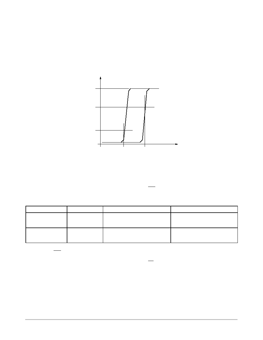
Input Schmitt Triggers
All the Logic Input pins have built≠in Schmitt trigger
circuits to prevent the NCN6000 against uncontrolled
operation. The typical dynamic characteristics of the related
pins are depicted in Figure 33.
The output signal is guaranteed to go High when the input
voltage is above 0.70*Vbat, and will go Low when the input
voltage is below 0.30*Vbat.
The CLOCK_IN pin has been design to provide a 40 MHz
bandwidth clock receiver input, capable to drive the internal
clock divider. This front end circuit yields a constant Duty
Cycle signal, according to the ISO specification, to the
external smart card, even when the NCN6000 division ratio
is 1:1.
Output
V
bat
ON
OFF
V
bat
0.70
*V
bat
Figure 33. Typical Schmitt Trigger Characteristic
Input
0.30
*V
bat
Interrupt Function
The NCN6000 flags the external microprocessor by pulling down the INT signal provided in pin 9. This signal is activated
by one of the here below referenced operations.
Table 6. Interrupt Functions
Pin Related
Clear Function
STATUS Pin 5
Card Insertion and
Extraction
11
Positive Going Chip Select, or logical
combination of Chip Select Low and
PWR_ON Positive Going
High = Card Presents
Low = No Card Inserted
DC/DC Converter
Overloaded
15
Positive Going Chip Select, or logical
combination of Chip Select Low and
PWR_ON Positive Going
High = DC/DC Operates Normally
Low = Output CRD_VCC Overloaded
Leaving the INT pin Low has no influence on the
NCN6000 internal behavior. It is up to the engineering to
decide when and how the interrupt will be cleared from this
pin. As described before, this can be achieved by either
providing a Chip Select positive transient, or by starting the
DC/DC converter with the standard command PWR_ON =
H and CS =L.

NCN6000
http://onsemi.com
31
Security Features
In order to protect both the interface and the external smart
card, the NCN6000 provides security features to prevent
catastrophic failures as depicted here after.
Pin Current Limitation: In the case of a short circuit to
ground, the current forced by the device is limited to 15 mA
for any pins, except CRD_CLK pin. No feedback is
provided to the external MPU.
DC/DC Operation: The internal circuit continuously
senses the CRD_VCC voltage and, in the case of either over
or undervoltage situation, update the STATUS register
accordingly. This register can be read out by the MPU.
Battery Voltage: Both the Over and Undervoltage are
detected by the NCN6000, a POWER_DOWN sequence
and the STATUS register being updated accordingly. The
external MPU can read the STATUS pin to take whatever is
appropriate to cope with the situation.
ESD Protection
The NCN6000 includes silicon devices to protect the pins
against the ESD spikes voltages. To cope with the different
ESD voltages developed across these pins, the built≠in
structures have been designed to handle either 2.0 kV, when
related to the microcontroller side, or 8.0 kV when
connected with the external contacts. Practically, the
CRD_RST, CRD_CLK, CRD_IO and CRD_DET pins can
sustain 8 kV, the digital pins being capable to sustain 2 kV.
The CRD_VCC pin has the same 8 kV ESD protection, but
can source up to 55 mA continuously, the absolute
maximum current being 100 mA.
To save as much battery current as possible when no card
is inserted, one should use a Normally Open Card Detection
switch connected pin 11. Since the internal card detection
circuit source 10
mA (typical) to bias the switch, using a
Normally Open avoid this direct sink to ground from the
battery.
Parallel Operation
When two or more NCN6000 operate in parallel on a
common digital bus, the Chip Select pin allows the selection
of one chip from the bank of the paralleled devices. Of
course, the external MPU shall provide one unique CS line
for each of the NCN6000 considered interfaces. When a
given interface is selected by CS = L, all the logic inputs
becomes active, the chip can be programmed or/and the
external card can be accessed. When CS = H, all the input
logic pins are in the high impedance state, thus leaving the
bus available for other purpose. On the other hand, when
CS = H, the CRD_IO and CRD_RST hold the previous I/O
and RESET logic state, the CRD_CLK being either active
or stopped, according to the programmed state forced by the
MPU.
Since there is one single I/O line to communicate with the
external microcontroller, one should provide a software
routine to save the code when data exchanged are performed
between the two cards. Generally speaking, the internal
microcontroller RAM can be used to support such a
transaction.
The CRD_VCC voltage and CRD_CLK signal of each
NCN6000 can be operated simultaneously, these two pins
being activated even when the related chip select is High. As
depicted in Figure 14, the DC/DC converter is not
deactivated when PWR_ON goes to Low when CS = High.
Minimum Power Consumption
To achieve a minimum current consumption, the interface
shall be programmed as follow:
1. Turn off the DCDC converter : this will disconnect
the smart card if still inserted in the socket),
reducing the power supply to the minimum needed
to control the interface.
2. Force the input signals to a logic High to avoid
current flowing through the pull up resistors. This
applies to the here below table:
INT
Pin 9
CS
Pin 6
STATUS
Pin 5
I/O
Pin 8
CRD_IO
Pin 14
To save as much battery current as possible when no card
is inserted, one should use a Normally Open Card Detection
switch connected pin 11 to ground. Since the internal card
detection circuit source is 10
mA (typical), using such a NO
switch saves the direct sink to ground current from the
battery to ground.
During this mode of operation, the only active sub
functions are the card detection and the battery monitoring.
The activity resume immediately after either a card
insertion, or a CS = Low signal applied to pin 6.
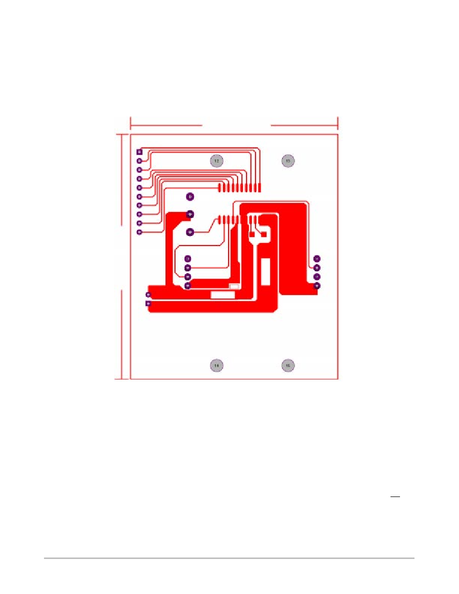
NCN6000
http://onsemi.com
32
Printed Circuit Board Layout
Since the NCN6000 carries high speed currents together
with high frequency clock, the printed circuit board must be
carefully designed to avoid the risk of uncontrolled
operation of the interface.
A typical single≠sided PCB layout is provided in
Figure 34 highlighting the ground technique.
The card socket uses a low cost ISO only version, all the
parts being located on the Component side. Connector J3
makes reference to the microcontroller used by the final
application. Of course, the connector is not necessary and
standard copper tracks might be used to connect the MPU to
the NCN6000 interface chip.
2335 mis (60 mm)
2760 mis (70 mm)
U1
NCN6000
SMARTCARD ISO CONTACTS
MPU
V
supply
+V
bat
C4
CLK
RST
GROUND
C8
I/O
V
PP
GND
Figure 34. Typical Single Sided Printed Circuit Board Layout
Application Note
A partial schematic diagram of the demo board designed
to support the NCN6000 applications is depicted in
Figure 35. This schematic diagram highlights the interface
between the microcontroller and the Smart Card, leaving
aside the peripherals used to control the MPU.
Conclusion
From a practical stand point, the CRD_VCC output
capacitor has been split into two 6.8
mF/10 V/X7R, one
being located as close as possible across pins 13 and 17 of
the NCN6000, the second one being located close by the
smart card physical connector. On the other hand, care has
been observed to minimize the cross coupling between the
clock signals (both Input and CRD_CLK) and the other
signals presents on the board.
The microcontroller holds the software necessary to
program the NCN6000, together with the code handling the
T0 operation. Provisions are made to provide a
communication link with an external computer by using the
RS232 standard port.
Due to the Chip Select signal, several NCN6000 can share
a common data bus as depicted in Figure 36. In this example,
two interfaces are connected to a single MPU, the CS pins
being controlled by two different signals.
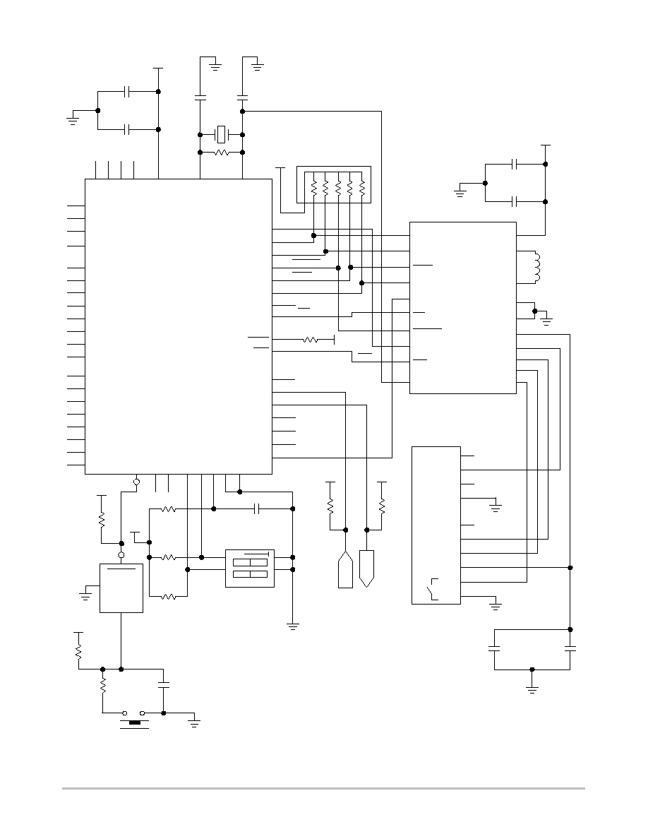
NCN6000
http://onsemi.com
33
Figure 35. NCN6000 Single Interface Demo Board
GND
PC0
PC1
PC2
PC3
PC4
PC5
PC7
XIRQ
PC6
L1
22
µ
H
1
2
3
4
5
6
7
8
9
10
20
19
18
17
16
15
14
13
12
11
A0
A1
PGM
PWR_ON
STATUS
CS
RESET
I/O
INT
CLOCK_IN
V
bat
L
out_H
L
out_L
PWR_GND
GROUND
CRD_V
CC
CRD_IO
CRD_CLK
CRD_RST
CRD_DET
C2
SMARTCARD_B
J2
ISO7816
GND
NCN6000
VCC
10
µ
F/6.3 V
U1
C1
C9
4.7
µ
F/10 V
A0
A1
PGM
PWR_ON
STATUS
CS
RESET
I/O
CLK
C8
I/O
VPP
GND
C4
CLK
RST
VCC
Swb
E
PD0/RXD
PD1/TD
PD2
9
10
11
12
13
14
15
16
20
19
5
20
21
22
PA4
PA5
PA6
PA7
XT
AL
30
29
28
27
IN
RESET
GND
C11
2.2
µ
F
16 V
RESET
SW13
U5
MC34164
C10
4.7
µ
F/10 V
GND
0.1
µ
F/25 V
Swa
8
7
6
5
4
3
2
1
18
17
GND
GND
IRQ
R7 4.7k
VCC
16
INT
PD3
23
PD4
24
PD5
25
TX
RX
R8
4.7k
R10
4.7k
VCC
VCC
VSS
VRL
VRH
MODB
MODA
C4
0.1
µ
F/25 V
R14
10 R
GND
R20
4.7 k
R21
4.7 k
VCC
51
52
2
4
3
6
STRA
STRB
RST
17
1
R9
4.7k
VCC
R16
220 R
VCC
GND
R16
220 R
GND
1
3
2
1
2
3
4
5
6
VCC
R6
10 M
C6
22 pF
C7
22 pF
Y1
8 MHz
GND
GND
VCC
C2
0.1
µ
F/25 V
GND
10
µ
F/6.3 V
C1
EXT
AL
26
7
8
VDD
PA
0
PA
1
PA
2
PA
3
34
33
32
31
PE0
PE1
PE2
PE3
43
45
47
49
PE4
PE5
PE6
PE7
44
46
48
50
PB7
PB6
PB5
PB4
35
36
37
38
PB3
PB2
PB1
PB0
39
40
41
42
U1
68HC11E9
SW DIP≠2
1 = Mode B
2 = Mode A
S?
R1 10k

NCN6000
http://onsemi.com
34
Figure 36. NCN6000 Single Interface Demo Board
GND
PC0
PC1
PC2
PC3
PC4
PC5
PC7
XIRQ
PC6
L1
22
µ
H
1
2
3
4
5
6
7
8
9
10
20
19
18
17
16
15
14
13
12
11
A0
A1
PGM
PWR_ON
STATUS
CS
RESET
I/O
CLOCK_IN
V
bat
L
out_H
L
out_L
PWR_GND
GROUND
CRD_V
CC
CRD_IO
CRD_CLK
CRD_RST
CRD_DET
C2
GND
VCC
10
µ
F/6.3 V
U1
C1
A0
A1
PGM
PWR_ON
STATUS
CS
RESET
I/O
C8
I/O
VPP
GND
C4
CLK
RST
VCC
Swb
E
PD0/RXD
PD1/TD
PD2
9
10
11
12
13
14
15
16
20
19
5
20
21
22
PA4
PA5
PA6
PA7
XT
AL
30
29
28
27
IN
RESET
GND
C11
2.2
µ
F
16 V
RESET
SW13
U5
MC34164
GND
0.1
µ
F/25 V
Swa
8
7
6
5
4
3
2
1
18
17
GND
GND
IRQ
R5 4.7k
16
PD3
23
PD4
24
PD5
25
TX
RX
R6
4.7k
R7
4.7k
VCC
VCC
VSS
VRL
VRH
MODB
MODA
C5
0.1
µ
F/25 V
R8
10 R
GND
R9
4.7 k
R10
4.7 k
VCC
51
52
2
4
3
6
STRA
STRB
RST
17
1
R4
4.7k
VCC
R16
220 R
GND
R16
220 R
GND
1
3
2
1
2
3
4
5
6
VCC
R6
10 M
C6
22 pF
C7
22 pF
Y1
8 MHz
GND
GND
VCC
C2
0.1
µ
F/25 V
GND
10
µ
F/6.3 V
C1
EXT
AL
26
7
8
VDD
PA
0
PA
1
PA
2
PA
3
34
33
32
31
PE0
PE1
PE2
PE3
43
45
47
49
PE4
PE5
PE6
PE7
44
46
48
50
PB7
PB6
PB5
PB4
35
36
37
38
PB3
PB2
PB1
PB0
39
40
41
42
U1
68HC11E9
SW DIP≠2
1 = Mode B
2 = Mode A
S1
A0
A1
PGM
PWR_ON
STATUS
CS
RESET
I/O
INT
CLOCK_IN
V
bat
L
out_H
L
out_L
PWR_GND
GROUND
CRD_V
CC
CRD_IO
CRD_CLK
CRD_RST
CRD_DET
NCN6000
U1
CLK
VCC
INT
L1
22
µ
H
1
2
3
4
5
6
7
8
9
10
20
19
18
17
16
15
14
13
12
11
A0
A1
PGM
PWR_ON
ST
A
TUS
CS
RESET
I/O
INT
CLOCK_IN
V
bat
L
out_H
L
out_L
PWR_GND
GROUND
CRD_V
CC
CRD_IO
CRD_CLK
CRD_RST
CRD_DET
1
2
3
4
5
6
7
8
9
A0
A1
PGM
PWR_ON
ST
A
TUS
CS
RESET
I/O
INT
CLOCK_IN
V
bat
L
out_H
L
out_L
PWR_GND
GROUND
CRD_V
CC
CRD_IO
CRD_CLK
CRD_RST
CRD_DET
ISO7816
SMAR
TCARD_B
J2
R2 10k
GND
C8
I/O
VPP
GND
C4
CLK
RST
VCC
Swb
Swa
8
7
6
5
4
3
2
1
18
17
ISO7816
SMARTCARD_B
J2
U1
NCN6000
GND
C10 4.7
µ
F/10 V
C9 4.7
µ
F/10 V
NCN6000
http://onsemi.com
35
Summary
Subject
Page
PIN FUNCTIONS AND DESCRIPTION
6
MAXIMUM RATINGS
8
POWER SUPPLY SECTION
9
DIGITAL PARAMETERS SECTION
10
SMART CARD INTERFACE SECTION
11
PROGRAMMING AND STATUS FUNCTIONS
12
CARD VCC, CARD CLOCK AND CARD
DETECTION POLARITY PROGRAMMING
13
DC/DC CONVERTER AND CARD DETECTOR
STATUS
14
CARD POWER SUPPLY TIMINGS
14
BASIC OPERATING MODE FLOW CHART
15
STANDBY MODE
15
PROGRAMMING MODE
16
ACTIVE MODE
16
TRANSACTION MODE
17
IDLE MODE
17
CARD POWER DOWN MODE
17
CARD DETECTION
19
POWER MANAGEMENT
21
VBAT SUPPLY VOLTAGE MONITORING
22
DC/DC CONVERTER OPERATION
22
CLOCK DIVIDER
25
BIDIRECTIONNAL LEVEL SHIFTER
29
INPUT SCHMITT TRIGGERS
30
INTERRUPT FUNCTIONS
30
SECURITY FEATURES
31
ESD PROTECTION
31
MULTI CARD PARALLEL OPERATION
31
MINIMUM POWER CONSUMPTION
31
PRINTED CIRCUIT BOARD LAYOUT
32
APPLICATION NOTE
32
PACKAGE OUTLINE DIMENSIONS
36
CONCLUSION
32
Figure Index
Fig. #
Title
Page
1
Simplified Application Diagram
1
2
Typical Application Diagram
2
3
Block Diagram
3
4
Programming and Normal Operation Basic
Timing
4
5
Interrupt Servicing and Card Polling
5
6
Card Power Supply Turn ON and OFF
Timing
14
7
Operating Modes Flow Chart
15
8
Minimum Programming Timings
16
9
Typical Power Down Sequence in the
NCN6000 Interface
18
10
Power Down Sequence Details
18
11
Card Insertion Detection and Interrupt
Signals
19
12
Card Extraction Detection and Interrupt
Signals
20
13
Interrupt Acknowledgement during a Card
Insertion Detection Sequence.
20
14
Card Power Supply Control
21
15
Smart Card Signals Sequence at Power On
21
16
Typical Vbat Monitoring
22
17
Basic DC/DC Structure
22
18
DCDC Operating Modes
23
19
Typical DC Operating Current
23
20
Typical Y7R Ceramic Type Value as a
Function of the Temperature.
23
21
CRD_VCC Ripple as a Function of the
Capacitor Technology
24
22
External Capacitor Current Charge and
CRD_VCC Voltage Ripple
24
23
CRD_VCC Voltage Ripple
24
24
Simplified Frequency Divider and
Programming Functions
25
25
Clock Programming Examples
26
26
Command Stop Clock HIGH
27
27
Command Stop Clock LOW
27
28
Command Resume Clock Normal Operation
28
29
Card Clock Rise and Fall Time
28
30
Basic internal I/O Level Shifter
29
31
Typical CRD_IO Rise Time
29
32
Typical I/O and RST Signals During an ATR
Sequence
29
33
Typical Schmitt Trigger Characteristic
30
34
Typical Single Sided Printed Circuit Board
Layout
32
35
NCN6000 Single Interface Demo Board
33
36
Typical Dual Interface Application
34

NCN6000
http://onsemi.com
36
PACKAGE DIMENSIONS
TSSOP≠20
DTB SUFFIX
CASE 948E≠02
ISSUE A
DIM
A
MIN
MAX
MIN
MAX
INCHES
6.60
0.260
MILLIMETERS
B
4.30
4.50
0.169
0.177
C
1.20
0.047
D
0.05
0.15
0.002
0.006
F
0.50
0.75
0.020
0.030
G
0.65 BSC
0.026 BSC
H
0.27
0.37
0.011
0.015
J
0.09
0.20
0.004
0.008
J1
0.09
0.16
0.004
0.006
K
0.19
0.30
0.007
0.012
K1
0.19
0.25
0.007
0.010
L
6.40 BSC
0.252 BSC
M
0 8 0 8
_
_
_
_
NOTES:
1. DIMENSIONING AND TOLERANCING PER ANSI
Y14.5M, 1982.
2. CONTROLLING DIMENSION: MILLIMETER.
3. DIMENSION A DOES NOT INCLUDE MOLD FLASH,
PROTRUSIONS OR GATE BURRS. MOLD FLASH
OR GATE BURRS SHALL NOT EXCEED 0.15
(0.006) PER SIDE.
4. DIMENSION B DOES NOT INCLUDE INTERLEAD
FLASH OR PROTRUSION. INTERLEAD FLASH OR
PROTRUSION SHALL NOT EXCEED 0.25 (0.010)
PER SIDE.
5. DIMENSION K DOES NOT INCLUDE DAMBAR
PROTRUSION. ALLOWABLE DAMBAR
PROTRUSION SHALL BE 0.08 (0.003) TOTAL IN
EXCESS OF THE K DIMENSION AT MAXIMUM
MATERIAL CONDITION.
6. TERMINAL NUMBERS ARE SHOWN FOR
REFERENCE ONLY.
7. DIMENSION A AND B ARE TO BE DETERMINED
AT DATUM PLANE -W-.
ÕÕÕÕ
ÕÕÕÕ
ÕÕÕÕ
1
10
11
20
PIN 1
IDENT
A
B
≠T≠
0.100 (0.004)
C
D
G
H
SECTION N≠N
K
K1
J J1
N
N
M
F
≠W≠
SEATING
PLANE
≠V≠
≠U≠
S
U
M
0.10 (0.004)
V
S
T
20X REF
K
L
L/2
2X
S
U
0.15 (0.006) T
DETAIL E
0.25 (0.010)
DETAIL E
6.40
0.252
---
---
S
U
0.15 (0.006) T
ON Semiconductor and are registered trademarks of Semiconductor Components Industries, LLC (SCILLC). SCILLC reserves the right to make
changes without further notice to any products herein. SCILLC makes no warranty, representation or guarantee regarding the suitability of its products for any
particular purpose, nor does SCILLC assume any liability arising out of the application or use of any product or circuit, and specifically disclaims any and all
liability, including without limitation special, consequential or incidental damages. "Typical" parameters which may be provided in SCILLC data sheets and/or
specifications can and do vary in different applications and actual performance may vary over time. All operating parameters, including "Typicals" must be
validated for each customer application by customer's technical experts. SCILLC does not convey any license under its patent rights nor the rights of others.
SCILLC products are not designed, intended, or authorized for use as components in systems intended for surgical implant into the body, or other applications
intended to support or sustain life, or for any other application in which the failure of the SCILLC product could create a situation where personal injury or death
may occur. Should Buyer purchase or use SCILLC products for any such unintended or unauthorized application, Buyer shall indemnify and hold SCILLC
and its officers, employees, subsidiaries, affiliates, and distributors harmless against all claims, costs, damages, and expenses, and reasonable attorney fees
arising out of, directly or indirectly, any claim of personal injury or death associated with such unintended or unauthorized use, even if such claim alleges that
SCILLC was negligent regarding the design or manufacture of the part. SCILLC is an Equal Opportunity/Affirmative Action Employer.
PUBLICATION ORDERING INFORMATION
JAPAN: ON Semiconductor, Japan Customer Focus Center
2≠9≠1 Kamimeguro, Meguro≠ku, Tokyo, Japan 153≠0051
Phone: 81≠3≠5773≠3850
Email: r14525@onsemi.com
ON Semiconductor Website: http://onsemi.com
For additional information, please contact your local
Sales Representative.
NCN6000/D
Literature Fulfillment:
Literature Distribution Center for ON Semiconductor
P.O. Box 5163, Denver, Colorado 80217 USA
Phone: 303≠675≠2175 or 800≠344≠3860 Toll Free USA/Canada
Fax: 303≠675≠2176 or 800≠344≠3867 Toll Free USA/Canada
Email: ONlit@hibbertco.com
N. American Technical Support: 800≠282≠9855 Toll Free USA/Canada