
©
Semiconductor Components Industries, LLC, 2003
July, 2003 - Rev. 2
1
Publication Order Number:
NCN6001/D
NCN6001
Compact Smart Card
Interface IC
The NCN6001 is an integrated circuit dedicated to the smart card
interface applications. The device handles any type of smart card
through a simple and flexible microcontroller interface. On top of that,
thanks to the built-in chip select pin, several couplers can be
connected in parallel.
The device is particularly suited for low cost, low power
applications, with high extended battery life coming from extremely
low quiescent current.
Features
∑
100% Compatible with ISO 7816-3, EMV and GIE-CB Standards
∑
Fully GSM Compliant
∑
Wide Battery Supply Voltage Range: 2.7 < V
CC
< 5.5 V
∑
Programmable CRD_VCC Supply Handles 1.8 V, 3.0 V or 5.0 V
Card Operation
∑
Programmable Rise and Fall Card Clock Slopes
∑
Programmable Card Clock Divider
∑
Built-in Chip Select Logic Allows Parallel Coupling Operation
∑
ESD Protection on Card Pins (8.0 kV, Human Body Model)
∑
Supports up to 40 MHz Input Clock
∑
Built-in Programmable CRD_CLK Stop Function Handles Run or
Low State
∑
Programmable CRD_CLK Slopes to Cope with Wide Operating
Frequency Range
∑
Fast CRD_VCC Turn-on and Turn-off Sequence
Typical Applications
∑
E-Commerce Interface
∑
Automatic Teller Machine (ATM) Smart Card
∑
Point of Sales (POS) System
∑
Pay TV System
Device
Package
Shipping
ORDERING INFORMATION
NCN6001DTBR2
TSSOP - 20
2500 Tape & Reel
TSSOP - 20
DTB SUFFIX
CASE 948E
1
20
MARKING
DIAGRAM
A = Assembly Location
L
= Wafer Lot
Y = Year
W = Work Week
PIN CONNECTIONS
1
2
3
4
5
6
7
8
20
19
18
16
15
14
13
(Top View
)
CLK_SPI
I/O
INT
CLK_IN
MOSI
EN_RPU
MISO
CS
Lout_H
GND
CRD_VCC
CRD_CLK
CRD_IO
NCN
6001
ALYW
1
20
9
10
11
12
17
V
CC
Lout_L
PWR_GND
CRD_RST
CRD_DET
C8/S1
C4/S0
http://onsemi.com

NCN6001
http://onsemi.com
2
12
13
20
18
GND
L1
22
m
H
9
1
2
3
4
5
7
8
6
10
19
17
16
15
14
11
Swa
Swb
C8
C4
CLK
RST
V
CC
GND
I/O
17
18
7
4
3
2
1
5
8
SMARTCARD_C
ISO7816
GND
GND
GND
NCN6001
10
m
F
U1
Figure 1. Typical Application
CLK_SPI
CLK_IN
MOSI
EN_RPU
MISO
CS
Lout_H
GND
CRD_VCC
CRD_CLK
CRD_IO
Lout_L
CRD_RST
CRD_DET
C8/S1
C4/S0
V
CC
I/O
INT
V
CC
PWR_GND
GND
C2
10
m
F
J1
C1
MICROCONTROLLER
V
CC
R1
47 k
CRD_DET
GROUND
3
9
1
2
6
10
5
8
7
15
11
19
17
16
12
EN_RPU
MOSI
CLK_SPI
CS
MISO
I/O
INT
CLK_IN
Lout_H
Lout_L
PWR_GND
CRD_VCC
CLOCK
DIVIDER
4
INTERRUPT BLOCK
DC/DC CONVER
TER
GND
13
14
Figure 2. Block Diagram
PROGRAMMABLE
CARD DETECTION
18
DUAL 8
-
BIT
SHIFT REGISTER
V
CC
ADDRESS DECODING
LOGIC CONTROL
ISO7816 SEQUENCER
CARD PINS DRIVER
20
C4/S0
C8/S1
CRD_RST
CRD_CLK
CRD_IO
b7
b6
b5
b4
b3
b2
b1
b0
b3
b2
b7
b6
b5
b4
b1
b0
GND
20 k
V
CC
50 k
CRD_VCC
20 k
V
CC
500 k
3 States

NCN6001
http://onsemi.com
3
PIN FUNCTIONS AND DESCRIPTION
Pin
Name
Type
Description
1
I/O
Input/Output
Pull Up
This pin is connected to an external microcontroller interface. A bidirectional level
translator adapts the serial I/O signal between the smart card and the microcontroller.
The level translator is enabled when CS = L, the sub address has been selected and
the system operates in the Asynchronous mode. When a Synchronous card is in use,
this pin is disconnected and the data and the transaction take place with the MISO b3
register.
The internal pull up resistor connected on the
m
C side is activated and visible by the
selected chip only.
2
INT
OUTPUT
Pull Up
This pin is activated LOW when a card has been inserted and detected by CRD_DET
pin. Similarly, an interrupt is generated when the CRD_VCC output is overloaded, or
when the card has been extracted whatever be the transaction status (running or
stand by).
The INT signal is reset to High according to Table 7 and Figure 11. On the other hand,
the pin is forced to a logic High when the input voltage V
CC
drops below 2.0 V.
3
CLK_IN
CLOCK INPUT
High impedance
The built - in Schmitt trigger receiver makes this pin suitable for a large type of clock
signal (Figure 30). This pin can be connected to either the microcontroller master
clock, or to a crystal signal, to drive the external smart cards. The signal is fed to the
internal clock selector circuit and translated to the CRD_CLK pin at either the same
frequency, or divided by 2 or 4, depending upon the programming mode.
Note: The chip guarantees the EMV 50% Duty Cycle when the clock divider ratio is
1/2 or
1/4
, even when the CLK_IN signal is out of the 45% to 55% range specified by
ISO and EMV specifications.
Care must be observed, at PCB level, to minimize the pick - up noise coming from the
CLK_IN line.
4
MOSI
INPUT
Master Out Slave In: SPI Data Input from the external microcontroller. This byte
contents the address of the selected chip among the four possible, together with the
programming code for a given interface.
5
CLK_SPI
INPUT
Clock Signal to synchronize the SPI data transfer. The built - in Schmitt trigger receiver
makes this pin compatible with a wide range of input clock signal (Figure 30). This
clock is fully independent from the CLK_IN signal and does not play any role with the
data transaction.
6
EN_RPU
INPUT, Logic
This pin is used to activate the I/O internal pull up resistor according to the here below
true table:
EN_RPU = Low
I/O Pull Up resistor disconnected
EN_RPU = High
I/O Pull Up resistor connected
When two or more NCN6001 chips shares the same I/O bus, one chip only shall have
the internal pull up resistor enabled to avoid any overload of the I/O line.
Moreover, when Asynchronous and Synchronous cards are handled by the interfaces,
the activated I/O pull up resistor must preferably be the one associated with the
Asynchronous circuit
.
On the other hand, since no internal pull up bias resistor is built in the chip, pin 6 must
be connected to the right voltage level to make sure the logic function is satisfied.
7
MISO
OUTPUT
Master In Slave Out: SPI Data Output from the NCN6001. This byte carries the state
of the interface, the serial transfer being achieved according to the programmed mode
(Table 2), using the same CLK_SPI signal and during the same MOSI time frame. The
three high bits [b7:b5] have no meaning and shall be discarded by the microcontroller.
An external 4.7 k
W
Pull down resistor might be necessary to avoid misunderstanding
of the pin 7 voltage during the High Z state.
8
CS
INPUT
This pin synchronizes the SPI communication and provides the chip address and
selected functions.
All the NCN6001 functions, both programming and card transaction, are disabled
when CS = H.

NCN6001
http://onsemi.com
4
PIN FUNCTIONS AND DESCRIPTION (continued)
Pin
Description
Type
Name
9
V
CC
POWER
This pin is connected to the NCN6001 supply voltage and must be bypassed to
ground by a 10
m
F/6.0 V capacitor.
Since tantalum capacitors have relative high ESR, using low ESR ceramic type
(MURATA X5R, Resr < 100 m
W
) is highly recommended.
10
Lout_H
POWER
The High Side of the external inductor is connected between this pin and Lout_L/pin
12 to provide the DC/DC function. The current flowing into this inductor is internally
sensed and no external shunt resistor is used. Typically, Lout = 22
m
H, with ESR <
2
.0
W
, yields a good efficiency performance for a maximum 65 mA DC output load.
Note: The inductor shall be sized to handle the 450 mA peak current flowing during the
DC/DC operation (see CoilCraft manufacturer data sheet).
11
PWR_GND
POWER
This pin is the Power Ground associated with the built - in DC/DC converter and must
be connected to the system ground together with GROUND pin 16. Using good quality
ground plane is recommended to avoid spikes on the logic signal lines.
12
Lout_L
POWER
The High Side of the external inductor is connected between this pin and Lout_H to
activate the DC/DC function. The built - in NMOS and PMOS devices provide the
switching function together with the CRD_VCC voltage rectification (Figure 17).
13
CRD_VCC
POWER
This pin provides the power to the external card. It is the logic level "1" for CRD_IO,
CRD_RST, CRD_C4, CRD_C8 and CRD_CLK signals.
The energy stored by the DC/DC external inductor Lout must be smoothed by a
10
m
F/Low ESR capacitor, connected across CRD_VCC and GND. Using ceramic
type of capacitor (MURATA X5R, ESR < 50 m
W
) is strongly recommended. In the
event of a CRD_VCC U
VLOW
voltage, the NCN6001 detects the situation and
feedback the information in the STATUS bit. The device does not take any further
action, particularly the DC/DC converter is neither stopped nor re programmed by the
NCN6001. It is up to the external MPU to handle the situation.
However, when the CRD_VCC is overloaded, the NCN6001 shuts off the DC/DC
converter, runs a Power Down ISO sequence and reports the fault in the STATUS
register.
Since high transient current flows from this pin to the load, care must be observed, at
PCB level, to minimize the series ESR and ESL parasitic values. The NCN6001 demo
board provides an example of a preferred PCB layout.
14
C8/S0
I/O
Auxiliary mixed analog/digital line to handle either a synchronous card, or as Chip
Select Identification (MISO, Bit 0): see Figure 9. The pin is driven by an open drain
stage, the pull up resistor being connected to the CRD_VCC supply. When the pin is
used as a logic input (asynchronous cards), the positive logic condition applies:
Connected to GND
Logic = Zero
Connected to V
CC
or left Open
Logic = One
A built - in accelerator circuit makes sure the output positive going rise time is fully
within the ISO/EMV specifications.
NOTE:
The pin is capable of reading the logic level when the chip operates an
asynchronous interface, but is not intended to read the data from the
external card when operated in the synchronous mode. It merely returns the
logic state forced during a write instruction to the card.
15
C4/S1
I/O
Auxiliary mixed analog/digital line to handle either a synchronous card, or as Chip
Select Identification (MISO, Bit 1): see Figure 9. The pin is driven by an open drain
stage, the pull up resistor being connected to the CRD_VCC supply. When the pin is
used as a logic input (asynchronous cards), the positive logic condition applies:
Connected to GND
Logic = Zero
Connected to V
CC
or left Open
Logic = One
A built - in accelerator circuit makes sure the output positive going rise time is fully
within the ISO/EMV specifications.
NOTE:
The pin is capable of reading the logic level when the chip operates an
asynchronous interface, but is not intended to read the data from the
external card when operated in the synchronous mode. It merely returns the
logic state forced during a write instruction to the card.

NCN6001
http://onsemi.com
5
PIN FUNCTIONS AND DESCRIPTION (continued)
Pin
Description
Type
Name
16
GROUND
SIGNAL
The logic and low level analog signals shall be connected to this ground pin. This pin
must be externally connected to the PWR_GND pin 12. The designer must make sure
no high current transients are shared with the low signal currents flowing into this pin.
17
CRD_CLK
OUTPUT
This pin is connected to the CLK pin of the card connector. The CRD_CLK signal
comes from the clock selector circuit output. An internal active pull down NMOS
device forces this pin to Ground during either the CRD_VCC start up sequence, or
when CRD_VCC = 0 V.
The rise and fall slopes, either FAST or SLOW, of this signal can be programmed by
the MOSI message (Table 2).
Care must be observed, at PCB level, to minimize the pick - up noise coming from the
CRD_CLK line.
18
CRD_DET
INPUT
The signal coming from the external card connector is used to detect the presence of
the card. A built - in pull up low current source biases this pin High, making it active
LOW, assuming one side of the external switch is connected to ground. A built - in
digital filter protect the system against voltage spikes present on this pin.
The polarity of the signal is programmable by the MOSI message, according to the
logic state depicted Table 2. On the other hand, the meaning of the feedback message
contained in the MISO register bit b4, depends upon the SPI mode of operation as
defined here below:
SPI Normal Mode: The MISO bit b4 is High when a card is inserted, whatever be the
polarity of the card detect switch.
SPI Special Mode: The MISO bit b4 copies the logic state of the Card detect switch as
depicted here below, whatever be the polarity of the switch used to handle the
detection:
CRD_DET = Low
MISO/b4 = Low
CRD_DET = High
MISO/b4 = High
In both cases, the chip must be programmed to control the right logic state (Table 2).
Since the bias current supplied by the chip is very low, typically 5.0
m
A, care must be
observed to avoid low impedance or cross coupling when this pin is in the Open state.
19
CRD_RST
OUTPUT
This pin is connected to the RESET pin of the card connector. A level translator adapts
the RESET signal from the microcontroller to the external card. The output current is
internally limited to 15 mA.
The CRD_RST is validated when CS = Low and hard wired to Ground when the card
is deactivated, by and internal active pull down circuit.
Care must be observed, at PCB design level, to avoid cross coupling between this
signal and the CRD_CLK clock.
20
CRD_IO
I/O
Pull Up
This pin handles the connection to the serial I/O pin of the card connector. A
bidirectional level translator adapts the serial I/O signal between the card and the
microcontroller. An internal active pull down MOS device forces this pin to Ground
during either the CRD_VCC start up sequence, or when CRD_VCC = 0 V. The
CRD_IO pin current is internally limited to 15 mA.
Care must be observed, at PCB design level, to avoid cross coupling between this
signal and the CRD_CLK clock.

NCN6001
http://onsemi.com
6
MAXIMUM RATINGS
(Note 1)
Rating
Symbol
Value
Unit
Power Supply Voltage
V
CC
6.0
V
Power Supply Current
Note: This current represents the maximum peak current the
pin can sustain, not the NCN6001 average consumption.
I
bat
500
mA
Power Supply Current
I
CC
150 (Internally Limited)
mA
Digital Input Pins
V
in
- 0.5 V < V
in
< V
CC
+0.5 V,
but < 6.0 V
V
Digital Input Pins
I
in
"
5.0
mA
Digital Output Pins
V
out
- 0.5 V < V
in
< V
CC
+0.5 V,
but < 6.0 V
V
Digital Output Pins
I
out
"
10
mA
Card Interface Pins
V
card
- 0.5 V < V
card
< CRD_VCC +0.5 V
V
Card Interface Pins, excepted CRD_CLK
I
card
15 (Internally Limited)
mA
Inductor Current
I
Lout
500 (Internally Limited)
mA
ESD Capability (Note 2)
Standard Pins
Card Interface Pins
CRD_DET
V
ESD
2.0
8.0
4.0
kV
kV
kV
TSSOP - 20 Package
Power Dissipation @ Tamb = +85
∞
C
Thermal Resistance, Junction - to - Air (R
q
JA
)
P
DS
R
q
JA
320
125
mW
∞
C/W
Operating Ambient Temperature Range
T
A
- 25 to +85
∞
C
Operating Junction Temperature Range
T
J
- 25 to +125
∞
C
Maximum Junction Temperature (Note 3)
T
Jmax
+150
∞
C
Storage Temperature Range
T
stg
- 65 to +150
∞
C
1. Maximum electrical ratings are defined as those values beyond which damage to the device may occur at T
A
= +25
∞
C.
2. Human Body Model, R = 1500
W
, C = 100 pF.
3. Absolute Maximum Rating beyond which damage to the device may occur.

NCN6001
http://onsemi.com
7
DIGITAL PARAMETERS
@ 2.7 V < V
CC
< 5.5 V ( - 25
∞
C to +85
∞
C ambient temperature, unless otherwise noted).
Note: Digital inputs undershoot < - 0.3 V to ground, Digital inputs overshoot < 0.3 V to V
CC
.
Rating
Pin
Symbol
Min
Typ
Max
Unit
Input Asynchronous Clock Duty Cycle = 50%
@ V
CC
= 3.0 V Over the Temperature Range
@ V
CC
= 5.0 V Over the Temperature Range
3
F
CLKIN
-
-
-
-
30
40
MHz
Input Clock Rise Time
Input Clock Fall Time
3
F
tr
F
tf
2.5
2.5
-
-
-
-
ns
ns
Input SPI Clock
5
F
CLKSPI
-
-
15
MHz
Input CLK_SPI Rise/Fall Time @ Cout = 30 pF
5
tr
spi
, tf
spi
-
-
12
ns
Input MOSI Rise/Fall Time @ Cout = 30 pF
4
tr
mosi
,
tf
mosi
-
-
12
ns
Output MISO Rise/Fall Time @ Cout = 30 pF
7
tr
miso
,
tf
miso
-
-
12
ns
Input CS Rise/Fall Time
8
tr
str
, tf
str
-
-
12
ns
I/O Data Transfer Switching Time, both directions
(I/O and CRD_IO), @ Cout = 30 pF
I/O Rise Time * (Note 4)
I/O Fall Time
1, 20
t
RIO
t
FIO
-
-
-
-
0.8
0.8
m
s
m
s
INT Pull Up Resistance
2
R
ITA
20
50
80
k
W
Positive Going Input High Voltage Threshold
(CLK_IN, MOSI, CLK_SPI, EN_RPU, CS)
2, 3, 4, 5,
6, 8
V
IA
0.70 * V
CC
-
V
CC
V
Negative Going Input High Voltage Threshold
(CLK_IN, MOSI, CLK_SPI, EN_RPU, CS)
2, 3, 4, 5,
6, 8
V
ILLA
0
-
0.3 * V
CC
V
Output High Voltage
INT, MISO @ O
H
= - 10
m
A
2, 7
V
OH
V
CC
- 1.0 V
-
V
CC
V
Output Low Voltage
INT, MISO @ O
H
= 200
m
A
2, 7
V
OL
-
-
0.4
V
Delay Between Two Consecutive CLK_SPI Sequence
5
td
clk
33
-
-
ns
4. Since a 20 k
W
(typical) pull up resistor is provided by the NCN6001, the external MPU can use an Open Drain connection. On the other hand,
NMOS smart cards can be used straightforward.

NCN6001
http://onsemi.com
8
POWER SUPPLY
@ 2.7 V < V
CC
< 5.5 V ( - 25
∞
C to +85
∞
C ambient temperature, unless otherwise noted).
Rating
Pin
Symbol
Min
Typ
Max
Unit
Input Power Supply
9
V
CC
2.70
-
5.50V
V
Standby Supply Current Conditions:
INT = CLK_IN = CLK_SPI = CS = H
I/O = MOSI = EN_RPU = H, No Card Inserted
V
CC
= 3.0 V
V
CC
= 5.0 V
9
Icc
sb
-
-
25
35
50
60
mA
DC Operating Current
CLK_IN = Low, All Card Pins Unloaded
@ V
CC
= 3.3 V, CRD_VCC = 5.0 V
@ V
CC
= 5.5 V, CRD_VCC = 5.0 V
9
Icc
op
-
-
-
-
0.5
1.5
mA
V
CC
Under Voltage Detection
High
V
CC
Under Voltage Detection
Low
V
CC
Under Voltage (Note 7)
9
VCC
LH
VCC
LL
VCC
POR
2.20
2.00
1.50
-
-
-
2.70
2.60
2.20
V
Output Card Supply Voltage
@ 2.7 V < V
CC
< 5.5 V
CRD_VCC = 1.8 V @ Iload = 35 mA
CRD_VCC = 3.0 V @ Iload = 60 mA
CRD_VCC = 5.0 V @ Iload = 65 mA
13
V
C2H
V
C3H
V
C5H
1.65
2.75
4.75
-
1.80
3.00
5.00
1.95
3.25
5.25
V
Maximum Continuous Output Current
@ CRD_VCC = 1.8 V
@ CRD_VCC = 3.0 V
@ CRD_VCC = 5.0 V
13
Icc
35
60
65
-
-
-
-
-
-
mA
Output Over Current Limit
V
CC
= 3.3 V, CRD_VCC = 1.8 V, 3.0 V or 5.0 V
V
CC
= 5.0 V, CRD_VCC = 1.8 V, 3.0 V or 5.0 V
13
Iccov
-
-
100
150
-
-
mA
Output Dynamic Peak Current
@ CRD_VCC = 1.8 V, 3.0 V or 5.0 V, Cout = 10
m
F
(Notes 5 and 6)
13
Iccd
100
-
-
mA
Output Card Supply Voltage Ripple
@ V
CC
= 3.6 V, Lout = 22
m
H, Cout1 = Cout2 = 4.7
m
F
Ceramic X7R, Iout = 55 mA
CRD_VCC = 5.0 V
(Note 5)
CRD_VCC = 3.0 V
CRD_VCC = 1.8 V
13
-
-
-
-
35
35
35
-
-
-
mV
Output Card Supply Turn On Time @
Lout = 22
m
F, Cout1 = 10
m
F Ceramic
V
CC
= 2.7 V, CRD_VCC = 5.0 V
13
Vcc
TON
-
-
500
m
s
Output Card Supply Shut Off Time @
Cout1 = 10
m
F, Ceramic
V
CC
= 2.7 V, CRD_VCC = 5.0 V, VCC
OFF
< 0.4 V
13
Vcc
TOFF
-
100
250
m
s
5. Ceramic X7R, SMD type capacitors are mandatory to achieve the CRD_VCC specifications. When an electrolytic capacitor is used, the
external filter must include a 220 nF, max 50 m
W
ESR capacitor in parallel, to reduce both the high frequency noise and ripple to a minimum.
Depending upon the PCB layout, it might be necessary to use two 4.7
m
F/6.0 V/ceramic/X5R/SMD 0805 in parallel, yielding an improved
CRD_VCC ripple over the temperature range.
6. Pulsed current, according to ISO7816 - 3, paragraph 4.3.2.
7. No function externally available during the V
CC
POR sequence.

NCN6001
http://onsemi.com
9
SMART CARD INTERFACE
@ 2.7 V < V
CC
< 5.5 V ( - 25
∞
C to +85
∞
C ambient temperature, unless otherwise noted).
Note: Digital inputs undershoot < - 0.3 V to ground, Digital inputs overshoot < 0.3 V to V
CC
.
Rating
Pin
Symbol
Min
Typ
Max
Unit
CRD_RST @ CRD_VCC = 1.8 V, 3.0 V, 5.0 V
Output RESET V
OH
@ Irst = - 200
m
A
Output RESET V
OL
@ Irst = 200
m
A
Output RESET Rise Time @ Cout = 30 pF
Output RESET Fall Time @Cout = 30 pF
19
V
OH
V
OL
t
R
t
F
CRD_VCC - 0.5
0
-
-
-
-
-
-
CRD_VCC
0.4
100
100
V
V
ns
ns
CRD_CLK as a function of CRD_VCC
CRD_VCC = +5.0 V or 3.0 V or 1.8V
Output Frequency
Output V
OH
@ Icrd_clk = - 200
m
A
Output V
OL
@ Icrd_clk = 200
m
A
CRD_CLK Output Duty Cycle
CRD_VCC = 5.0 V
CRD_VCC = 3.0 V
CRD_VCC = 1.8 V (Note 8)
Rise & Fall time @ CRD_VCC = 1.80 V to 5.0 V
Fast Mode
Output CRD_CLK Rise time @ Cout = 30 pF
Output CRD_CLK Fall time @ Cout = 30 pF
Rise & Fall time @ CRD_VCC = 1.80 V to 5.0 V
Slow Mode
Output CRD_CLK Rise time @ Cout = 30 pF
Output CRD_CLK Fall time @ Cout = 30 pF
17
F
CRDCLK
V
OH
V
OL
F
CRDDC
t
ress
t
fcs
t
rills
t
ulsa
-
CRD_VCC ≠ 0.5
0
45
40
40
-
-
-
-
2.1
1.9
11.5
10.8
20
CRD_VCC
+0.4
55
60
60
4
4
16
16
MHz
V
V
%
%
%
ns
ns
ns
ns
CRD_IO @ CRD_VCC = 1.8 V 3.0 V, 5.0 V
CRD_IO Data Transfer Frequency
CRD_IO Rise time @ Cout = 30 pF
CRD_IO Fall time @ Cout = 30 pF
Output V
OH
@ Icrd_clk = - 20
m
A
Output V
OL
@ Icrd_clk = 500
m
A, V
IL
= 0 V
20
F
IO
t
RIO
t
FIO
V
OH
V
OL
-
-
-
CRD_VCC
-
0.5
0
400
-
-
-
-
-
0.8
0.8
CRD_VCC
0.4
kHz
m
s
m
s
V
V
CRD_IO Pull Up Resistor
20
R
CRDPU
14
20
26
k
W
CRD_C8 Output Rise and Fall Time @ Cout = 30 pF
14
t
RC8,
t
FC8
-
-
100
ns
CRD_C4 Output Rise and Fall Time @ Cout = 30 pF
15
t
RC4,
t
FC4
-
-
100
ns
CRD_C4 and CRD_C8 Data Transfer Frequency
14, 15
F
C48
-
400
-
kHz
CRD_C8, CRD_C4 Output Voltages
High Level @ Irst = - 200
m
A
Low Level @ Irst = +200
m
A
14, 15
V
OH,
V
OL
CRD_VCC ≠ 0.5
0
-
-
-
0.4
V
V
C8/S0 and C4/S0 Address Bias Current (Note 9)
14, 15
I
bc4c8
-
1.0
-
m
A
Card Detection Digital Filter Delay:
Card Insertion
Card Extraction
18
T
CRDIN
T
CRDOFF
25
25
50
50
150
150
m
s
m
s
8. Parameter guaranteed by design, function 100% production tested.
9. Depending upon the environment, using and external pull up resistor might be necessary to cope with PCB surface leakage current.

NCN6001
http://onsemi.com
10
SMART CARD INTERFACE (continued)
@ 2.7 V < V
CC
< 5.5 V ( - 25
∞
C to +85
∞
C ambient temperature, unless otherwise noted).
Note: Digital inputs undershoot < - 0.3 V to ground, Digital inputs overshoot < 0.3 V to V
CC
.
Rating
Pin
Symbol
Min
Typ
Max
Unit
Card Insertion or Extraction Positive Going Input
High Voltage
18
V
IHDET
0.70 * V
CC
-
V
CC
V
Card Insertion or Extraction Negative Going Input
Low Voltage
18
V
ILDET
0
-
0.30 * V
CC
V
Card Detection Bias Pull Up Current @ V
CC
= 5.0 V
18
I
DET
-
10
-
m
A
Output Peak Max Current Under Card Static
Operation Mode @ CRD_VCC = 3.0 V or = 5.0 V
CRD_RST, CRD_IO, CRD_C4, CRD_C8
1, 20
Icrd_iorst
-
-
15
mA
Output Peak Max Current Under Card Static
Operation Mode @ CRD_VCC = 3.0 V or = 5.0 V
CRD_CLK
17
Icrd_clk
-
-
70
mA

NCN6001
http://onsemi.com
11
PROGRAMMING
Write Register
"
WRT_REG
The WRT_REG register handles three command bits
[b5:b7] and five data bits [b0:b4] as depicted in Table 1.
These bits are concatenated into a single byte to accelerate
the programming sequence. The register can be updated
when CS is low only.
The CRD_RST pin reflects the content of the MOSI
WRT_REG[b4] during the chip programming sequence.
Since this bit shall be Low to address the internal register of
the chip, care must be observed as this signal will be
immediately transferred to the CRD_RST pin.
Table 1. WRT_REG Bits Definitions
b0
b1
If (b7 + b6 + b5) <> 110 and (b7 + b6 + b5) <> 101 and (b7 + b6 + b5) <> 111 then
Case 00
CRD_VCC = 0 V
Case 01
CRD_VCC = 1.8 V
Case 10
CRD_VCC = 3.0 V
Case 11
CRD_VCC = 5.0 V
Else if (b7 + b6 + b5) = 110 then
b1 drives C4
b0 drives C8
Else if (b7 + b6 + b5) = 101 then
Case (b4 + b3 + b2 + b1 + b0) = 0000
CRD_DET = NO
Case (b4 + b3 + b2 + b1 + b0) = 0001
CRD_DET = NC
Case (b4 + b3 + b2 + b1 + b0) = 0010
SPI_MODE = Special
Case (b4 + b3 + b2 + b1 + b0) = 0011
SPI_MODE = Normal
End if
b2
b3
If (b7 + b6 + b5) <> 110 and (b7 + b6 + b5) <> 101 and (b7 + b6 + b5) <> 111 then
Case 00
CRD_CLK = L
Case 01
CRD_CLK = CLK_IN
Case 10
CRD_CLK = CLK_IN/2
Case 11
CRD_CLK = CLK_IN/4
Else if (b7 + b6 + b5) = 110 then
b3 drives CRD_CLK
b2 drives CRD_IO
Else if (b7 + b6 + b5) = 101 then
Case (b4 + b3 + b2 + b1 + b0) = 0000
CRD_DET = NO
Case (b4 + b3 + b2 + b1 + b0) = 0001
CRD_DET = NC
Case (b4 + b3 + b2 + b1 + b0) = 0010
SPI_MODE = Special
Case (b4 + b3 + b2 + b1 + b0) = 0011
SPI_MODE = Normal
End if
b4
Drives CRD_RST pin (Note 11)
b5,
b6,
b7
000
Select Asynchronous Card #0 (Note 10), four chips bank CS signal
001
Select Asynchronous Card #1 (Note 10), four chips bank CS signal
010
Select Asynchronous Card #2 (Note 10), four chips bank CS signal
011
Select Asynchronous Card #3 (Note 10), four chips bank CS signal
100
Select External Asynchronous Card, dedicated CS signal
110
Select External Synchronous Card, dedicated CS signal
101
Set Card Detection Switch polarity, Set SPI_MODE normal or special. Set CRD_CLK slopes Fast or Slow.
111
Reserved for future use
10. When operating in Asynchronous mode, [b5:b7] are compared with the external voltage levels present pins C4/S0 and C8/S1 (respectively
pins 15 and 14).
11. The CRD_RST pin reflects the content of the MOSI WRT_REG[b4] during the chip programming sequence. Since this bit shall be Low to
address the internal register of the chip, care must be observed as this signal will be immediately transferred to the CRD_RST pin.

NCN6001
http://onsemi.com
12
Table 2. WRT_REG Bits Definitions and Functions
ADDRESS
PARAMETERS
CHIP
BANK
MOSI bits
[b3:b2]
MOSI bits
[b1:b0]
MOSI bits
[b7:b0]
1
b7
b6
b5
b4
b3
b2
b1
b0
CRD_CLK
CRD_VCC
CRD_DET
1
0
X
X
RST
0
0
0
0
Low
0
-
1
0
X
X
RST
0
1
0
1
1/1
1.8 V
-
1
0
X
X
RST
1
0
1
0
1/2
3.0 V
-
1
0
X
X
RST
1
1
1
1
1/4
5.0 V
-
1
1
0
1
0
0
0
0
0
-
-
NO
1
1
0
1
0
0
0
0
1
-
-
NC
1
1
0
1
0
0
0
1
0
-
-
Special
1
1
0
1
0
0
0
1
1
-
-
Normal
1
1
0
1
0
0
1
0
0
-
-
SLO_SLP
1
1
0
1
0
0
1
0
1
-
-
FST_SLP
1
1
1
1
-
-
-
-
-
-
-
RFU
2
1
0
0
RST
0
0
0
0
Low
0
-
2
1
0
0
RST
0
1
0
1
1/1
1.8 V
-
2
1
0
0
RST
1
0
1
0
1/2
3.0 V
-
2
1
0
0
RST
1
1
1
1
1/4
5.0 V
-
2
1
1
0
RST
CLK
I/O
C4
C8
-
-
Data to Sync. Card
2
1
0
1
0
0
0
0
0
-
-
NO
2
1
0
1
0
0
0
0
1
-
-
NC
2
1
0
1
0
0
0
1
0
-
-
Special
2
1
0
1
0
0
0
1
1
-
-
Normal
2
1
0
1
0
0
1
0
0
-
-
SLO_SLP
2
1
0
1
0
0
1
0
1
-
-
FST_SLP
2
1
1
1
-
-
-
-
-
-
-
RFU
12. Chip Bank 1 = Asynchronous cards, four slots addresses 1 to 4.
Chip Bank 2 = Asynchronous or synchronous card, single slot.
13. Address 101 and bits [b0 : b4] not documented in the table are reserved for future use.
Address 111 is reserved for future use.
Although using the %111XXXXX code is harmless from
a NCN6001 silicon standpoint, care must be observed to
avoid uncontrolled operation of the interface sharing the
same digital bus. When this code is presented on the digital
bus, the CRD_RST signal of any interface sharing the CS
signal, immediately reflects the digital content of the MOSI
bit b4 register. Similarly, the MISO register of the shared
interface is presented on the SPI port. Consequently, data
collision, at MISO level, and uncontrolled card operation are
likely to happen if the system uses a common Chip Select
line. It is strongly recommended to run a dedicated CS bit to
any external circuit intended to use the $111xxxxx code.
On the other hand, the CRD_RST signal will be forced to
Low when the internal register of the chip is programmed to
accommodate different hardware conditions (NO/NC,
Special/Normal, SLO_SLP/FST_SLP). Generally speaking,
such a configuration shall take place during the Power On
Reset to avoid CRD_RST activation.

NCN6001
http://onsemi.com
13
Read Register
"
READ_REG
The READ_REG register contains the data read from the
interface and from the external card. The selected register is
transferred to the MISO pin during the MOSI sequence
(CS = Low). Table 3 gives the bits definition.
Depending upon the programmed SPI_MODE, the
content of READ_REG is transferred on the MISO line
either on the Positive going (SPI_MODE = Special) or upon
the Negative going slope (SPI_MODE = Normal) of the
CLK_SPI signal. The external microcontroller shall discard
the three high bytes since they carry no valid data.
Table 3. MOSI and MISO Bits Identifications and Functions
MOSI
b7
b6
b5
b4
b3
b2
b1
b0
Operating Mode
0
0
0
0
1
1
0
0
1
1
0
1
0
1
0
1
0
0
RST
RST
RST
RST
RST
RST
CLK
CLK
CLK
CLK
CLK
CLK
CLK
CLK
CLK
CLK
CLK
I/O
V
CC
V
CC
V
CC
V
CC
V
CC
C4
V
CC
V
CC
V
CC
V
CC
V
CC
C8
Asynchronous, Program Chip
Asynchronous, Program Chip
Asynchronous, Program Chip
Asynchronous, Program Chip
Asynchronous, Program Chip
Synchronous, Sets Card Bits
MISO
z
z
z
Card Detect
I/O
C4
C8
PWR Monitor
Read Back Data
ASYNCHRONOUS MODE
In this mode, the CRD_C4 and CRD_C8 pins are used to
define the physical addresses of the interfaces when a bank
of up to four NCN6001 share the same digital bus.
SYNCHRONOUS MODE
In this mode, CRD_C4 and CRD_C8 are connected to the
smart card and it is no longer possible to share the CS signal
with other device. Consequently, a dedicated Chip Select
signal must be provided when the interfaces operate in a
multiple operation mode (Figure 33).
On the other hand, since bits [b4 ≠ b0] of the MOSI
register contain the smart card data, programming the
CRD_VCC output voltage shall be done by sending a
previous MOSI message according to Table 1 and Table 2.
The CRD_RST pin reflects the content of the MOSI
WRT_REG[b4] during the chip programming sequence.
Since this bit shall be Low to address the internal register of
the chip, care must be observed as this signal will be
immediately transferred to the CRD_RST pin.
Since no physical address can exist when the chip operates
in this mode, the MOSI register must use the format
%100XXXXX to program the chip (%100 prefix, XXXXX
data).
Example:
LDAA #%10010111
;set RST = H, CLK = 1/1, VCC = 5.0 V
STAA
MOSI
LDAA #%11010011
;SYNC. Card: set RST = H, CLK = L, IO = L, C4 = H, C8= H
STAA
MOSI
LDAA #%00111110
;ASYNC. Card: set RST = H, CLK =
º, VCC = 3.0 V
STAA
MOSI

NCN6001
http://onsemi.com
14
START UP DEFAULT CONDITIONS
At start up, when the V
CC
power supply is turned on, the
internal POR circuit sets the chip in the default conditions as
defined in Table 4.
Table 4. Start Up Default Conditions
CRD_DET
Normally Open
CRD_VCC
Off
CRD_CLK
t
r
and t
f
= SLOW
CRD_CLK
Low
Protocol
Special Mode
CARD DETECTION
The card is detected by the external switch connected pin
18. The internal circuit provides a positive bias of this pin
and the polarity of the insertion/extraction is programmable
by the MOSI protocol as depicted in Table 2.
The bias current is 1.0
mA typical and care must be
observed to avoid leakage to ground from this pin to
maintain the logic function. In particular, using a low
impedance probe (< 1.0 M
W) may lead to uncontrolled
operation during the debug.
Depending upon the programmed condition, the card can
be detected either by a Normally Open (default condition) or
a Normally Close switch (Table 2). On the other hand, the
meaning of the feedback message contained in the MISO
register bit b4, depends upon the SPI mode of operation as
defined here below:
SPI Normal Mode: the MISO bit b4 is High when a card is
inserted, whatever be the polarity of the card detect switch.
SPI Special Mode: the MISO bit b4 copies the logic state of
the Card detect switch as depicted here below, whatever be
the polarity of the switch used to handle the detection:
CRD_DET = Low
MISO/b4 = Low
CRD_DET = High
MISO/b4 = High
CRD_VCC OPERATION
The built-in DC/DC converter provides the CRD_VCC
voltage and can be programmed to run one of the three
possible values, 1.8 V, 3.0 V or 5.0 V, assuming the input
voltage V
CC
is within the 2.7 V to 5.5 V range. In any case,
CRD_VCC is voltage regulated, together with a current
overload detection. On the other hand, the power conversion
is automatically switched to handle either a boost or a buck
mode of operation, depending upon the difference between
the input voltage V
CC
and the output supply CRD_VCC.
The CRD_VCC output current is a function of the V
CC
input value as depicted in Table 5.
Table 5. CRD_VCC Output Voltage Range
CRD_VCC
Comments
1.80 V
Maximum Output DC Current = 35 mA
3.0 V
Maximum Output DC Current = 60 mA
5.0 V
Maximum Output DC Current = 65 mA
Whatever the CRD_VCC output voltage may be, a
built-in comparator makes sure the voltage is within the
ISO7816-3/ EMV specifications. If the voltage is no longer
within the minimum/maximum values, the DC/DC is
switched Off, the Power Down sequence takes place and an
interrupt is presented at the INT pin 2.
POWER UP SEQUENCE
The Power Up Sequence makes sure all the card related
signals are Low during the CRD_VCC positive going slope.
These lines are validated when CRD_VCC is above the
minimum specified voltage (depending upon the
programmed CRD_VCC value).
Figure 3. Typical Start Up CRD_VCC Sequence

NCN6001
http://onsemi.com
15
At power up, the CRD_VCC voltage rise time depends
upon the current capability of the DC/DC converter
associated with the external inductor L1 and the reservoir
capacitor connected across CRD_VCC and GROUND.
During this sequence, the average input current is 300 mA
typical (Figure 3), assuming the system is fully loaded
during the start up. Finally, the application software is
responsible for the smart card signal sequence.
On the other hand, at turn off, the CRD_VCC fall time
depends upon the external reservoir capacitor and the peak
current absorbed by the internal NMOS transistor built
across CRD_VCC and GROUND. These behaviors are
depicted in Figure 4.
Since these parameters have finite values, depending
upon the external constraints, the designer must take care of
these limits if the t
ON
or the t
OFF
provided by the data sheets
does not meet his requirements.
Figure 4. CRD_VCC Typical Rise and Fall Time
Figure 5. Start Up Sequence with ATR

NCN6001
http://onsemi.com
16
POWER DOWN SEQUENCE
The NCN6001 provides an automatic Power Down
sequence, according to the ISO7816-3 specifications, and
the communication session terminates immediately. The
sequence is launched when the card is extracted, or when the
CRD_VCC voltage is overloaded as described by the
ISO/CEI 7816-3 sequence depicted hereafter:
ISO7816-3 sequence:
"
Force RST to Low
"
Force CLK to Low, unless it is already in this state
"
Force C4 & C8 to Low
"
Force CRD_IO to Low
"
Shut Off the CRD_VCC supply
Since the internal digital filter is activated for any card
insertion or extraction, the physical power sequence will be
activated 50
ms (typical) after the card has been extracted. Of
course, such a delay does not exist when the MPU
intentionally launches the power down. Figure 6 shows the
oscillogram captured in the NCN6001 demo board.
The internal active pull down NMOS connected across
CRD_VCC and GND discharges the external reservoir
capacitor in 100
ms (typical), assuming Cout = 10 mF.
Figure 6. Typical Power Down Sequence
Typical delay between each signal is 500 ns
The internal active pull down NMOS connected across CRD_VCC and GND discharges the external reservoir capacitor in
100
ms (typical), assuming Cout = 10 mF.

NCN6001
http://onsemi.com
17
DATA I/O LEVEL SHIFTER
The level shifter accommodates the voltage difference
that might exist between the microcontroller and the smart
card. A pulsed accelerator built-in circuit provides the fast
positive going transient according to the ISO7816-3
specifications. The basic I/O level shifter is depicted in
Figure 7.
LOGIC AND
LEVEL SHIFT
Q4
Q3
Q2
R2
18 k
Q5
GND
CRD_VCC
13
CRD_IO
20
CRD_VCC
CARD ENABLE
POR
SEQ 1
200 ns
200 ns
Q1
R1
18 k
EN_RPU
6
I/O
1
V
CC
9
V
CC
PMOS
U1
VCC
Q5
GND
SYNC
MOSI/b3
MOSI/b2
From MOSI
decoding
Figure 7. Basic I/O Internal Circuit
The transaction is valid when the Chip Select pin is Low,
the I/O signal being Open Drain or Totem Pole on either
sides.
Since the device can operate either in a single or a multiple
card system, provisions have been made to avoid CRD_IO
current overload. Depending upon the selected mode of
operation (ASYNC. or Sync), the card I/O line is
respectively connected to either I/O pin 1, or to the MOSI
register byte bit 2. On the other hand, the logic level present
at the card I/O is feedback to the
mC via the MISO register
bit 3. The logic level present at pin 6 controls the connection
of the internal pull up as depicted in Table 6.
Table 6. I/O Pull Up Resistor True Table
EN_RPU
I/O Pull Up Resistor
Device
Operation
Low
Open, 18 k
W
disconnected
Parallel Mode
High
Internal 18 k
W
pull up active
Single Device
NOTE:
18 k
W
typical value
Figure 8. Typical I/O Rise and Fall Time
NOTE: Both sides of the interface run with open drain load
(worst case condition).

NCN6001
http://onsemi.com
18
GENERAL PURPOSE CRD_C4 AND CRD_C8
These two pins can be used as a logic input to define the
address of a given interface (in the range $00 to $11), or as
a standard C4/C8 access to the smart card's channels. Since
these pins can be directly connected to the V
CC
power
supply, both output stages are built with switched
NMOS/PMOS totem pole as depicted in Figure 9.
Figure 9. Typical CRD_C4 Output Drive and Logic Control
Q1
U3
U4
GND
500 R
R1
CRD_VCC
C4
Q2
U1
LEVEL
SHIFTER
V
CC
WRT_C4
GND
Q3
ESD
SWITCHED
BIAS
U6
U9
I = 1 A
CONTROL
ADDRESS
READ_C4
U5
U8
U7
V
max
3
3
3
2
1
2
1
2
1
U2
V
CC
CRD_VCC
The C4 and C8 pins are biased by an internal current
source to provide a logic one when the pin is left open. In this
case, care must be observed to avoid relative low impedance
to ground to make sure the pin is at a High logic level.
However, it is possible to connect the pin to V
CC
(battery
supply) to force the logic input to a High level, regardless of
the input bias. Thanks to the CONTROL internal signal, the
system automatically adapts the mode of operation (chip
address or data communication) and, except the leakage, no
extra current is drawn from the battery to bias these pins
when the logic level is High.
When any of these pins is connected to GND, a continuous
1
mA typical sink current will be absorbed from the battery
supply.
The switched Totem Pole structure provides the fast
positive going transient when the related pin is forced to the
High state during a data transfer. In the event of a low
impedance connected across C4 or C8 to ground, the current
flow is limited to 15 mA, according to the ISO7816-3
specification.
The two general purpose pins can transfer data from the
external microcontroller to the card and read back the logic
state, but none of these pins can read the data coming from
the external smart card. On the other hand, both C4 and C8
can read input logic, hence the physical address of a given
chip.
In order to sustain the 8 kV ESD specified for these pins,
an extra protection structure Q3 has been implemented to
protect the MOS gates of the input circuit.

NCN6001
http://onsemi.com
19
INTERRUPT
When the system is powered up, the INT pin is set to High
upon POR signal. The interrupt pin 2 is forced LOW when
either a card is inserted/extracted, or when a fault is
developed across the CRD_VCC output voltage. This signal
is neither combined with the CS signal, nor with the chip
address. Consequently, an interrupt is placed on the
mC input
as soon as one of the condition is met.
The INT signal is clear to High upon one of the condition
given in Table 7.
Table 7. Interrupt Reset Logic
Interrupt Source
CS
CRD_VCC
Chip Address
Card Insertion
L
> 0
Selected Chip MOSI[b7 : B5] = 0xx or MOSI[b7 : B5] = 101
Card Insertion
L
= 0
Selected Chip MOSI[b7 :B5] = 0xx or MOSI[b7 : B5] = 101
Over Load
L
= 0
Selected Chip MOSI[b7 : B5] = 0xx or MOSI[b7 : B5] = 101
When several interfaces share the same digital
mC bus, it is up to the software to pool the chips, using the MISO register to
identify the source of the interrupt.
Figure 10. Basic Interrupt Function
CS
INT
CRD_DET
MOSI_b0
MOSI_b1
CRD_VCC > 0 V
CRD_VCC = 0 V
OVER LOAD
CRD_VCC
T0
T2
T10
T3
T4
T9
T6
T7
T8
T5
T1
T11
1
2
3
Table 8. Interrupt Reset Logic Operation
T0
A card has been inserted into the reader and detected by the CRD_DET signal. The NCN6001 pulls down the interrupt line.
T1
The
m
C sets the CS signal to Low, the chip is now active, assuming the right address has been placed by the MOSI register.
T2
The
m
C acknowledges the interrupt and resets the INT to High by the MOSI [B1 : B0 ] logic state: CRD_VCC is programmed
higher than zero volt.
T3
The card has been extracted from the reader, CRD_DET goes Low and an interrupt is set (INT = L). On the other hand, the
PWR_DOWN sequence is activated by the NCN6001.
T4
The interrupt pin is clear by the zero volt programmed to the interface.
T5
Same as T0
T6
The
m
C start the DC/DC converter, the interrupt is cleared (same as T2)
T7
An overload has been detected by the chip : the CRD_VCC voltage is zero, the INT goes Low.
T8
The card is extracted from the reader, CRD_DET goes Low and an interrupt is set (INT = L).
T9
The card is re - inserted before the interrupt is acknowledged by the
m
C: the INT pin stays Low.
T10
The
m
C acknowledges the interrupt and reset the INT to High by the MOSI [B1 : B0 ] logic state: CRD_VCC is programmed
higher than zero volt.
T11
The Chip Select signal goes High, all the related NCN6001 interface(s) are deactivated and no further programming or
transaction can take place.

NCN6001
http://onsemi.com
20
SPI PORT
The product communicates to the external
microcontroller by means of a serial link using a
Synchronous Port Interface protocol, the CLK_SPI being
Low or High during the idle state. The NCN6001 is not
intended to operate as a Master controller, but execute
commands coming from the MPU.
The CLK_SPI, the CS and the MOSI signals are under the
microcontroller's responsibility. The MISO signal is
generated by the NCN6001, using the CLK_SPI and CS
lines to synchronize the bits carried out by the data byte. The
basic timings are given in Figure 11 and Figure 12. The
system runs with two internal registers associated with the
MOSI and MISO data:
WRT_REG is a write only register dedicated to the MOSI
data.
READ_REG is a read only register dedicated to the MISO
data.
Figure 11. Basic SPI Timings and Protocol
MPU Asserts Chip Select
NCN6001 Reads Bit
MPU Reads Bit
RST_COUNTER
MOSI
SPI_CLK
CS
MISO
tclr
MPU Enables
Clock
MPU Sends Bit
NCN6001 Sends Bit
from READ_REG
When the CS line is High, no data can be written or read
on the SPI port. The two data lines becomes active when
CS = Low, the internal shift register is cleared and the
communication is synchronized by the negative going edge
of the CS signal. The data present on the MOSI line is
considered valid on the negative going edge of the CLK_SPI
clock and is transferred to the shift register on the next
positive edge of the same CLK_SPI clock.
To accommodate the simultaneous MISO transmit, an
internal logic identifies the chip address on the fly (reading
and decoding the three first bits) and validates the right data
present on the line. Consequently, the data format is MSB
first to read the first three signal as bits B5, B6 and B7. The
chip address is decoded from this logic value and validates
the chip according to the C4 and C8 conditions (Figure 12).
Figure 12. Chip Address Decoding Protocol and MISO Sequence
MPU Asserts Chip Set
MISO Line = High Impedance
ADDRESS
DECODE
MOSI
SPI_CLK
CS
MISO
MPU Enables Clock
B7
B6
B5
B4
B3
B2
B1
B0
LSB
COMMAND AND CONTROL
CHIP
ADDRESS
The Chip Address is decoded on the third clock pulse.
The MISO signal is activated and data transferred
MSB

NCN6001
http://onsemi.com
21
When the eight bits transfer is completed, the content of
the internal shift register is latched on the positive going
edge of the CS signal and the NCN6001 related functions are
updated accordingly.
Figure 13. Basic Multi Command SPI Bytes
Select Chip from SYNCHRONOUS Bank
Chip Ny
Chip Nx
tdclk
Special Mode: MISO
is synchronized with
the SPI_CLK Positive
going slope
Normal Mode: MISO is synchronized with
the SPI_CLK Negative going slope
MISO Line = High Impedance
MISO Line = High Impedance
B0
B1
B2
B3
B4
B5
B6
B7
B0
B1
B2
B3
B4
B5
B6
B7
SPI_CLK
CS
MOSI
SET_RST
SET_CLK
SET_VCC
ADDRESS
DECODE
CHIP
ADDRESS
COMMAND
AND CONTROL
MSB
MSB
LSB
LSB
MISO
Special Mode
MISO
Normal Mode
MPU Enables
Clock
Since the four chips present in the Asynchronous Bank
have an individual physical address, the system can control
several of these chips by sending the data content within the
same CS frame as depicted in Figure 13. The bits are
decoded on the fly and the related sub blocks are updated
accordingly. According to the SPI general specification, no
code or activity will be transferred to any chip when the CS
is High.
When two SPI bytes are sequentially transferred on the
MOSI line, the CLK_SPI sequence must be separated by at
least one half positive period of this clock (see td
clk
parameter).
The oscillograms shown in Figure 14 and Figure 15
illustrate the SPI communication protocol (source:
NCN6001 demo board).
Figure 14. Programming Sequence, Chip Address = $03

NCN6001
http://onsemi.com
22
Figure 15. MISO Read Out Sequences
Protocol: Special Mode
Protocol: Standard SPI
DC/DC OPERATION
The power conversion is based on a full bridge structure
capable to handle either step up or step down power supply
(Figure 16). The operation is fully automatic and, beside the
output voltage programming, does not need any further
adjustments.
Figure 16. Basic DC/DC Converter
G_Q4
G_Q2
G_Q7
G_HIZ
G_Q3
G_Q1
CMD_STOP
CMD_5.0V
CMD_3.0V
CMD_1.8V
GND
GND
GND
22
m
H
L1
GND
11
PWR_GND
10
m
F
C2
Q2
Q7
Q4
Q6
Q5
Q3
10
12
Q1
10
m
F
MIXED LOGIC/ANALOG BLOCK
V
CC
CRD_VCC
C1
13
6
In order to achieve the 250
ms max time to discharge
CRD_VCC to 400 mV called by the EMV specifications, an
active pull down NMOS is provided (Q7) to discharge the
external CRD_VCC reservoir capacitor. This timing is
guaranteed for a 10
mF maximum load reservoir capacitor
value (Figure 4).

NCN6001
http://onsemi.com
23
The system operates with a two cycles concept (all comments are referenced to Figure 16 and Figure 17):
1 - Cycle 1
Q1 and Q4 are switched ON and the inductor L1 is charged by the energy supplied by the external battery.
During this phase, the pair Q2/Q3 and the pair Q5/Q6 are switched OFF.
The current flowing the two MOSFET Q1 and Q4 is internally monitored and will be switched OFF when
the Ipeak value (depending upon the programmed output voltage value) is reached. At this point, Cycle 1 is
completed and Cycle 2 takes place. The ON time is a function of the battery voltage and the value of the induc-
tor network (L and Zr) connected across pins 10/11.
A 4
ms timeout structure ensures the system does run in a continuous Cycle 1 loop
2 - Cycle 2
Q2 and Q3 are switched ON and the energy stored into the inductor L1 is dumped into the external load
through Q2. During this phase, the pair Q1/Q4 and the pair Q5/Q6 are switched OFF.
The current flow period is constant (900 ns typical) and Cycle 1 repeats after this time if the CRD_VCC
voltage is below the specified value.
When the output voltage reaches the specified value (1.8 V, 3.0 V or 5.0 V), Q2 and Q3 are switched OFF
immediately to avoid over voltage on the output load. In the meantime, the two extra NMOS Q5 and Q6 are
switched ON to fully discharge any current stored into the inductor, avoiding ringing and voltage spikes over
the system. Figure 17 illustrates the theoretical waveforms present in the DC/DC converter.
CRD_VCC Charged
Figure 17. Theoretical DC/DC Operating Waveforms
I
peak
CRD_VCC
IL
Q5/Q6
Q2/Q3
Q1/Q4
V
ripple
CRD_VCC Voltage Regulated
t
off
t
on
Charge CRD_VCC
Next CRD_VCC Charge
(Time is Not to Scale)
When the CRD_VCC is programmed to zero volt, or when
the card is extracted from the socket, the active pull down Q7
rapidly discharges the output reservoir capacitor, making
sure the output voltage is below 0.4 V when the card slides
across the ISO contacts.
Based on the experiments carried out during the
NCN6001 characterization, the best comprise, at time of
printing this document, is to use two 4.7
mF/10 V/
ceramic/X7R capacitors in parallel to achieve the
CRD_VCC filtering. The ESR will not extend 50 m
W over
the temperature range and the combination of standard parts
provide an acceptable ≠20% to +20% tolerance, together
with a low cost. Table 9 gives a quick comparison between
the most common type of capacitors. Obviously, the
capacitor must be SMD type to achieve the extremely low
ESR and ESL necessary for this application. Figure 18
illustrates the CRD_VCC ripple observed in the NCN6001
demo board depending upon the type of capacitor used to
filter the output voltage.

NCN6001
http://onsemi.com
24
Table 9. Ceramic/Electrolytic Capacitors Comparison
Manufacturers
Type/Series
Format
Max Value
Tolerance
Typ. Z @ 500 kHz
MURATA
CERAMIC/GRM225
0805
10
m
F/6.3 V
- 20%/+20%
30 m
W
MURATA
CERAMIC/GRM225
0805
4.7
m
F/6.3 V
- 20%/+20%
30 m
W
VISHAY
Tantalum/594C/593C
-
10
m
F/16 V
-
450 m
W
VISHAY
Electrolytic/94SV
-
10
m
F/10 V
- 20%/+20%
400 m
W
-
Electrolytic Low Cost
-
10
m
F/10 V
- 35%/+50%
2.0
W
The DC/DC converter is capable to start with a full load
connected to the CRD_VCC output as depicted in Figure 19.
In this example, the converter is fully loaded when the
system starts from zero.
Figure 18. Typical CRD_VCC Ripple Voltage
Test Conditions: Cout = 2x 4.7
m
F/6 V/ceramic X7R,
Temp = +25
∞
C
Iout = Maximum Specification
Figure 19. Output Voltage Start - up Under Full
Load Conditions
58
60
62
64
66
68
70
72
74
2.5
3.0
3.5
4.0
4.5
5.0
5.5
Ef
f(%)
Figure 20. CRD_VCC Efficiency as a Function of the
Input Supply Voltage
V
bat
(V)
L
out
= 22
m
H/ESR = 2
W
V
out
= 3.0 V
V
out
= 5.0 V
V
out
= 1.8 V
The curves illustrate the typical behavior under full output
current load (35 mA, 60 mA and 65 mA), according to EMV
specifications.

NCN6001
http://onsemi.com
25
During the operation, the inductor is subject to high peak
current as depicted Figure 21 and the magnetic core must
sustain this level of current without damage. In particular,
the ferrite material shall not be saturated to avoid
uncontrolled current spike during the charge up cycle.
Moreover, since the DC/DC efficiency depends upon the
losses developed into the active and passive components,
selecting a low ESR inductor is preferred to reduce these
losses to a minimum.
Test Conditions: Input VCC voltage = 5.0 V
Current = 200 mA/div
Tamb = +20
∞
C
Figure 21. Typical Inductor Current
According to the ISO7816-3 and EMV specifications, the
interface shall limits the CRD_VCC output current to 200
mA maximum, under short circuit conditions. The
NCN6001 supports such a parameter, the limit being
depending upon the input and output voltages as depicted in
Figure 22.
On the other hand, the circuit is designed to make sure no
over current exist over the full temperature range. As a
matter of fact, the output current limit is reduced when the
temperature increases: see Figure 23.
0
20
40
60
80
100
120
140
160
180
2
3
4
5
6
Figure 22. Output Current Limits
V
bat
I
omax
= F (V
bat
)
V
o
= 3.0 V
V
o
= 5.0 V
V
o
= 1.8 V
I
out
100
110
120
130
140
150
160
- 25
- 5
15
35
55
75
95
115
TEMPERATURE (
∞
C)
I
out
(mA)
V
o
= 3.0 V
V
o
= 5.0 V
V
o
= 1.8 V
Figure 23. Output Current Limit as a Function of
the Temperature

NCN6001
http://onsemi.com
26
SMART CARD CLOCK DIVIDER
The main purpose of the built-in clock generator is
threefold:
1. Adapts the voltage level shifter to cope with the
different voltages that might exist between the
MPU and the Smart Card.
2. Provides a frequency division to adapt the Smart
Card operating frequency from the external clock
source.
3. Controls the clock state according to the smart
card specification.
In addition, the NCN6001 adjusts the signal coming from
the microprocessor to get the Duty Cycle window as defined
by the ISO7816-3 specification.
The byte content of the SPI port, B2 & B3, fulfills the
programming functions when CS is Low as depicted in
Figure 25 and Figure 24. The clock input stage (CLK_IN)
can handle a 20 MHz frequency maximum signal, the
divider being capable to provide a 1:4 ratio. Of course, the
ratio must be defined by the engineer to cope with the Smart
Card considered in a given application and, in any case, the
output clock [CRD_CLK] shall be limited to 20 MHz
maximum. In order to minimize the dI/dt and dV/dV
developed in the CRD_CLK line, the output stage includes
a special function to adapt the slope of the clock signal for
different applications
.
This function is programmed by the
MOSI register (Table 2: WRT_REG Bits Definitions and
Functions) whatever be the clock division.
In order to avoid any duty cycle out of the smart card
ISO7816-3 specification, the divider is synchronized by the
last flip flop, thus yielding a constant 50% duty cycle,
whatever be the divider ratio (Figure 24). Consequently, the
output CRD_CLK frequency division can be delayed by
four CLK_IN pulses and the microcontroller software must
take this delay into account prior to launch a new data
transaction. On the other hand, the output signal Duty Cycle
cannot be guaranteed 50% if the division ratio is 1 and if the
input Duty Cycle signal is not within the 46≠56% range.
The input signals CLK_IN and MOSI/b3 are
automatically routed to the level shifter and control block
according to the mode of operation.
CRD_CLK
CLOCK_IN
CLOCK : 2
CLOCK : 4
B2
B3
Clock is updated upon
These bits program
Internal
CLOCK programming is activated
by the B2 + B3 logic state
CLOCK = 1:1 ratio
CLOCK : 1
Figure 24. Typical Clock Divider Synchronization
CLOCK: 4 rising edge
CLOCK
Divider
Figure 25. Basic Clock Divider and Level Shifter
B1
B0
B3
B2
CLK_IN
VCC
CRD_CLK
CRD_VCC
LEVEL SHIFTER
AND CONTROL
Programming
CRD_CLK Slope
NOTE: Bits [B0...B3] come from SPI data
Programming
CRD_CLK
Division
SYNC
ASYNC
SYNC
U1
DIGITAL_MUX
OUT
SEL
A
B

NCN6001
http://onsemi.com
27
The input clock can be divided by 1/1,
Ω or º, depending
upon the specific application, prior to be applied to the smart
card driver. On the other hand, the positive and negative
going slopes of the output clock (CRD_CLK) can be
programmed to optimize the operation of the chip
(Table
10). The slope of the output clock can be
programmed on the fly, independently of either the
CRD_VCC voltage or the operating frequency, but care
must be observed as the CRD_RST will reflect the logic
state present at MOSI/b4 register.
Table 10. Output Clock Rise and Fall Time Selection
B0
B1
CRD_CLK
Division Ratio
CRD_CLK
SLO_SLP
CRD_CLK
FST_SLP
0
0
-
Output Clock = Low
Output Clock = Low
0
1
1
10 ns (typ.)
2 ns (typ.)
1
0
1/2
10 ns (typ.)
2 ns (typ.)
1
1
1/4
10 ns (typ.)
2 ns (typ.)
Figure 26. Force CRD_CLK to Low
Figure 27. Force CRD_CLK to Active Mode
Figure 28. CRD_CLK Programming
Note: Waveforms recorded without external compensation
network.
Figure 29. CRD_CLK Operating Low Speed (Top Trace),
Full Speed (Bottom Trace)

NCN6001
http://onsemi.com
28
INPUT SCHMITT TRIGGERS
All the Logic Input pins have built-in Schmitt trigger
circuits to protect the NCN6001 against uncontrolled
operation. The typical dynamic characteristics of the related
pins are depicted in Figure 30.
The output signal is guaranteed to go High when the input
voltage is above 0.70* V
CC
, and will go Low when the input
voltage is below 0.30* V
CC
.
Figure 30. Typical Schmitt Trigger Characteristic
OUTPUT
INPUT
V
bat
ON
OFF
0.3 V
bat
0.7 V
bat
V
bat
SECURITY FEATURES
In order to protect both the interface and the external smart
card, the NCN6001 provides security features to prevent
catastrophic failures as depicted hereafter.
Pin Current Limitation: In the case of a short circuit to
ground, the current forced by the device is limited to 15 mA
for any pins, except CRD_CLK pin. No feedback is
provided to the external MPU.
DC/DC Operation: The internal circuit continuously
senses the CRD_VCC voltage and, in the case of either over
or under voltage situation, updates the READ_REG register
accordingly and forces INT pin to Low. This register can be
read out by the MPU.
Battery Voltage: Both the over and under voltage are
detected by the NCN6001, the READ_REG register being
updated accordingly. The external MPU can read the register
through the MISO pin to take whatever is appropriate to
cope with the situation.
ESD PROTECTION
The NCN6001 includes silicon devices to protect the pins
against the ESD spikes voltages. To cope with the different
ESD voltages developed across these pins, the built-in
structures have been designed to handle either 2.0 kV, when
related to the microcontroller side, or 8.0 kV when
connected with the external contacts. Practically, the
CRD_RST, CRD_CLK, CRD_IO, CRD_C4, and CRD_C8
pins can sustain 8.0 kV, the maximum short circuit current
being limited to 15 mA. The CRD_VCC pin has the same
ESD protection, but can source up to 65 mA continuously,
the absolute maximum current being internally limited to
150 mA.
PRINTED CIRCUIT BOARD LAYOUT
Since the NCN6001 carries high speed currents together
with high frequency clock, the printed circuit board must be
carefully designed to avoid the risk of uncontrolled
operation of the interface.
A typical single sided PCB layout is provided in Figure 32
highlighting the ground technique. Dual face printed circuit
board may be necessary to solve ringing and cross talk with
the rest of the system.

NCN6001
http://onsemi.com
29
Figure 31. NCN6001 Engineering T
est Board Schematic Diagram
TEST BOARD SCHEMA
TIC DIAGRAM
U2
2
1
3
4
5
6
7
8
9
10
11
12
13
14
15
16
17
18
19
20
21
22
23
24
25
26
27
28
29
30
31
32
33
34
35
36
37
38
39
40
41
42
43
44
45
46
47
48
49
50
1
2
3
V
CC
V
CC
V
CC
V
CC
22
m
H
L1
R7
47 k
10
m
F
C2
GND
GND
Q1
R4
2.2 K
D4
GND
GND
GND
GND
R8
47 R
TP1
TP3
TP5
TP7
TP2
TP4
TP6
TP8
TP11 TP12 TP14
TP9
TP13
TP10
CRD_VCC
2N2222
GND
R6
47 k
C3
22 pF
4.7
m
F
C7
Swa
Swb
I/O
RST
CLK
C4
C8
V
CC
GND
I/O
CLK_IN
MISO
CLK_SP
V
CC
MOSI
EN_RPU
LoutL
CRD_DET
CRD_IO
CRD_RST
CRD_CLK
CRD_VCC
C4/S0
C8/S1
PWR_GND
LoutH
GND
R9
1 k
GND
GND
R5
4.7 k
CLK_SEL
J5
Demo Board
Identify NCN6001
J1
10
m
F
C1
GND
R1
2.2 k
GND
D1
CS
CLK_SP1
MOSI
MISO
I/O
INT
V
CC
GND
ISO7816
11
10
7
2
3
4
8
1
5
18
20
19
17
13
15
14
16
11
12
6
10
4
5
8
7
3
2
1
9
INT
CS
TP15
GND
J9
GROUND
2
1
1
INT
I/O
CLK_IN
CS
MISO
CLK_SP
MOSI
4.7
m
F
C8
J4
SMARTCARD_D
CRD_DET
CRD_IO
RST
CLK
RST
C4
C8
V
CC
See
Note
See
Note
CONTROL
AND
I/O
P1
EX_CLK
V
CC
NOTE:
Capacitor C2 and Resistor R8 are adjusted at final
checkout. Depending upon the PCB layout, these
two components may or may not be necessary
.

NCN6001
http://onsemi.com
30
Component Side (Top)
Copper Side (Bottom)
Top side
Figure 32. NCN6001 Demo Board Printed Circuit Board Layout

NCN6001
http://onsemi.com
31
Table 11. Demo Board Bill of Material
Desig.
Part Type
Footprint
Description
Supplier
Part Number
C1
10
m
F
1206
Capacitor
MURATA
GRM40 - X5R - 106K6.3
C2
10
m
F
1206
Capacitor
MURATA
GRM40 - X5R - 106K6.3
C3
22 pF
805
Capacitor
MURATA
C7
4.7
m
F
1206
Capacitor
MURATA
GRM40 - 034X5R - 475K6.3
C8
4.7
m
F
1206
Capacitor
MURATA
GRM40 - 034X5R - 475K6.3
D1
V
CC
SIP2
LED diode
Radio Spares
180 - 8467
D4
CRD_VCC
SIP2
LED diode
Radio Spares
180 - 8495
J1
CONTROL & I/O
IDC50
Fujitsu
FCN - 704Q050- AU/M
J4
SMARTCARD
SMARTCARD_ISO
Smart Card Connector
FCI
7434 - L01 - 35S01
J5
CLK_SEL
SIP3
Connector
J9
GROUND
GND_TEST
Connector
L1
22
m
H
1008
Inductor
CoilCraft
1008PS- 223 - M
P1
EX_CLK
SMB
SMB Connector
Radio Spares
112 - 2993
Q1
2N2222
TO - 18
NPN
ON Semiconductor
R1
2.2 k
805
Radio Spares
R4
2.2 k
805
Radio Spares
R5
4.7 k
805
Radio Spares
R6
47 k
805
Radio Spares
R7
47 k
805
Radio Spares
R8
47 R
805
Radio Spares
R9
1.0 k
805
Radio Spares
TP1
CLK_IN
TEST_POINT
TEST_POINT
Radio Spares
203 - 4910
TP10
RST
TEST_POINT
TEST_POINT
Radio Spares
203 - 4910
TP11
CLK
TEST_POINT
TEST_POINT
Radio Spares
203 - 4910
TP12
C4
TEST_POINT
TEST_POINT
Radio Spares
203 - 4910
TP13
C8
TEST_POINT
TEST_POINT
Radio Spares
203 - 4910
TP14
VCC
TEST_POINT
TEST_POINT
Radio Spares
203 - 4910
TP15
GND
TEST_POINT
TEST_POINT
Radio Spares
203 - 4910
TP2
INT
TEST_POINT
TEST_POINT
Radio Spares
203 - 4910
TP3
I/O
TEST_POINT
TEST_POINT
Radio Spares
203 - 4910
TP4
CS
TEST_POINT
TEST_POINT
Radio Spares
203 - 4910
TP5
MISO
TEST_POINT
TEST_POINT
Radio Spares
203 - 4910
TP6
CLK_SPI
TEST_POINT
TEST_POINT
Radio Spares
203 - 4910
TP7
MOSI
TEST_POINT
TEST_POINT
Radio Spares
203 - 4910
TP8
DET
TEST_POINT
TEST_POINT
Radio Spares
203 - 4910
TP9
CRD_IO
TEST_POINT
TEST_POINT
Radio Spares
203 - 4910
U1
NCN6001
ON Semiconductor
14. All resistors are
$
5%,
º
W , unless otherwise noted.
All capacitors are ceramic,
$
10%, 6.3 V, unless otherwise noted.

NCN6001
http://onsemi.com
32
Figure 33. Typical Multiple Parallel Interfaces
12
13
20
18
GND
9
1
2
3
4
5
7
8
6
10
19
17
16
15
14
11
Swa
Swb
C8
C4
CLK
RST
V
CC
GND
I/O
17
18
7
4
3
2
1
5
8
ISO7816
GND
GND
10
m
F
U1
CLK_SPI
CLK_IN
MOSI
EN_RPU
MISO
CS
Lout_H
GND
CRD_VC
C
CRD_CLK
CRD_IO
Lout_L
CRD_RST
CRD_DET
C8/S1
C4/S0
V
CC
I/O
INT
V
CC
PWR_GND
GND
C2
10
m
F
C1
STROBE_ASYNC
STROBE_SYNC
NCN6001
22
m
H
L1
MULTIPLE SMART CARD READER
12
13
20
18
9
1
2
3
4
5
7
8
6
10
19
17
16
15
14
11
Swa
Swb
C8
C4
CLK
RST
V
CC
GND
I/O
17
18
7
4
3
2
1
5
8
ISO7816
GND
U2
CLK_SPI
CLK_IN
MOSI
EN_RPU
MISO
CS
Lout_H
GND
CRD_VC
C
CRD_CLK
CRD_IO
Lout_L
CRD_RST
CRD_DET
C8/S1
C4/S0
V
CC
I/O
INT
PWR_GND
GND
C2
10
m
F
NCN6001
22
m
H
L2
12
13
20
18
9
1
2
3
4
5
7
8
6
10
19
17
16
15
14
11
Swa
Swb
C8
C4
CLK
RST
V
CC
GND
I/O
17
18
7
4
3
2
1
5
8
ISO7816
GND
U3
CLK_SPI
CLK_IN
MOSI
EN_RPU
MISO
CS
Lout_H
GND
CRD_VC
C
CRD_CLK
CRD_IO
Lout_L
CRD_RST
CRD_DET
C8/S1
C4/S0
V
CC
I/O
INT
PWR_GND
GND
C2
10
m
F
NCN6001
22
m
H
L3
12
13
20
18
9
1
2
3
4
5
7
8
6
10
19
17
16
15
14
11
Swa
Swb
C8
C4
CLK
RST
V
CC
GND
I/O
17
18
7
4
3
2
1
5
8
ISO7816
GND
U5
CLK_SPI
CLK_IN
MOSI
EN_RPU
MISO
CS
Lout_H
GND
CRD_VC
C
CRD_CLK
CRD_IO
Lout_L
CRD_RST
CRD_DET
C8/S1
C4/S0
V
CC
I/O
INT
PWR_GND
GND
C2
10
m
F
NCN6001
22
m
H
L4
V
CC
V
CC
V
CC
V
CC
12
13
20
18
9
1
2
3
4
5
7
8
6
10
19
17
16
15
14
11
Swa
Swb
C8
C4
CLK
RST
V
CC
GND
I/O
17
18
7
4
3
2
1
5
8
ISO7816
GND
U4
CLK_SPI
CLK_IN
MOSI
EN_RPU
MISO
CS
Lout_H
GND
CRD_VC
C
CRD_CLK
CRD_IO
Lout_L
CRD_RST
CRD_DET
C8/S1
C4/S0
V
CC
I/O
INT
PWR_GND
GND
C6
10
m
F
NCN6001
22
m
H
L5
V
CC
MICROCONTROLLER
SMARTCARD
J5
ASYNCHRONOUS
ASYNCHRONOUS
ASYNCHRONOUS
SMARTCARD
SMARTCARD
ASYNCHRONOUS
SMARTCARD
ASYNCHRONOUS
SMARTCARD
ADDRESS = $03
ADDRESS = $02
ADDRESS = $01
ADDRESS = $00
The five interfaces share a common microcontroller bus, a
bank of four NCN6001 supporting asynchronous card with a
dedicated CS line, the fifth one being used by to the synchronous
or asynchronous transactions with a unique CS line. On the
other hand, the only activated I/O pull up resistor shall be one
of the Asynchronous bank.

NCN6001
http://onsemi.com
33
Table of Contents
COMPACT SMART CARD INTERFACE IC
1
. . . . . . . . . . .
MAXIMUM RATINGS
6
. . . . . . . . . . . . . . . . . . . . . . . . . . . . . .
DIGITAL PARAMETERS SECTION
7
. . . . . . . . . . . . . . . . . .
POWER SUPPLY SECTION
8
. . . . . . . . . . . . . . . . . . . . . . . .
SMART CARD INTERFACE SECTION
9
. . . . . . . . . . . . . . .
PROGRAMMING
11
. . . . . . . . . . . . . . . . . . . . . . . . . . . . . . . . .
START UP DEFAULT CONDITIONS
14
. . . . . . . . . . . . . . . .
CARD DETECTION
14
. . . . . . . . . . . . . . . . . . . . . . . . . . . . . .
CRD_VCC OPERATION
14
. . . . . . . . . . . . . . . . . . . . . . . . . .
POWER UP SEQUENCE
14
. . . . . . . . . . . . . . . . . . . . . . . . .
POWER DOWN SEQUENCE
16
. . . . . . . . . . . . . . . . . . . . . .
DATA I/O LEVEL SHIFTER
17
. . . . . . . . . . . . . . . . . . . . . . . .
GENERAL PURPOSE CRD_C4 and CRD_C8
18
. . . . . . .
INTERRUPT
19
. . . . . . . . . . . . . . . . . . . . . . . . . . . . . . . . . . . . .
SPI PORT
20
. . . . . . . . . . . . . . . . . . . . . . . . . . . . . . . . . . . . . . .
DC/DC OPERATION
22
. . . . . . . . . . . . . . . . . . . . . . . . . . . . . .
SMART CARD CLOCK DIVIDER
26
. . . . . . . . . . . . . . . . . . .
INPUT SHITTY TRIGGERS
28
. . . . . . . . . . . . . . . . . . . . . . .
SECURITY FEATURES
28
. . . . . . . . . . . . . . . . . . . . . . . . . . .
ESD PROTECTION
28
. . . . . . . . . . . . . . . . . . . . . . . . . . . . . .
PRINTED CIRCUIT BOARD LAY OUT
28
. . . . . . . . . . . . . .
TEST BOARD SCHEMATIC DIAGRAM
29
. . . . . . . . . . . . .
ABBREVIATIONS
34
. . . . . . . . . . . . . . . . . . . . . . . . . . . . . . . .
DIMENSIONS
35
. . . . . . . . . . . . . . . . . . . . . . . . . . . . . . . . . . .
Figures Index
Figure 1. Typical Application
2
. . . . . . . . . . . . . . . . . . . . . . . .
Figure 2. Block Diagram
2
. . . . . . . . . . . . . . . . . . . . . . . . . . . .
Figure 3. Typical Start Up CRD_VCC Sequence
14
. . . . . .
Figure 4. CRD_VCC Typical Rise and Fall Time
15
. . . . . .
Figure 5. Start Up Sequence with ATR
15
. . . . . . . . . . . . . .
Figure 6. Typical Power Down Sequence
16
. . . . . . . . . . . .
Figure 7. Basic I/O Internal Circuit
17
. . . . . . . . . . . . . . . . . .
Figure 8. Typical I/O Rise and Fall Time
17
. . . . . . . . . . . . .
Figure 9. Typical CRD_C4 Output Drive and Logic Control
18
. . . . . . . . . . . . . . . . . . . . . . . . . . . . . . . . . . . . . . . . . . . . . . . . .
Figure 10. Basic Interrupt Function
19
. . . . . . . . . . . . . . . . . .
Figure 11. Basic SPI Timings and Protocol
20
. . . . . . . . . . .
Figure 12. Chip Address Decoding Protocol and MISO
Sequence
20
. . . . . . . . . . . . . . . . . . . . . . . . . . . . . . . . . . . . . . .
Figure 13. Basic Multi Command SPI Bytes
21
. . . . . . . . . .
Figure 14. Programming Sequence, Chip Address = $03
21
. . . . . . . . . . . . . . . . . . . . . . . . . . . . . . . . . . . . . . . . . . . . . . . . .
Figure 15. MISO Read Out Sequences
22
. . . . . . . . . . . . . .
Figure 16. Basic DC/DC Converter
22
. . . . . . . . . . . . . . . . . .
Figure 17. Theoretical DC/DC Operating Waveforms
23
. . . . . . . . . . . . . . . . . . . . . . . . . . . . . . . . . . . . . . . . . . . . . . . . .
Figure 18. Typical CRD_VCC Ripple Voltage
24
. . . . . . . . .
Figure 19. CRD_VCC Efficiency as a Function of the Input
Supply Voltage
24
. . . . . . . . . . . . . . . . . . . . . . . . . . . . . . . . . . .
Figure 20. CRD_VCC Efficiency as a Function of the Input
Supply Voltage
24
. . . . . . . . . . . . . . . . . . . . . . . . . . . . . . . . . . .
Figure 21. Typical Inductor Current
25
. . . . . . . . . . . . . . . . .
Figure 22. Output Current Limits
25
. . . . . . . . . . . . . . . . . . . .
Figure 23. Output Current Limit as a Function of the
Temperature
25
. . . . . . . . . . . . . . . . . . . . . . . . . . . . . . . . . . . . .
Figure 24. Typical Clock Divider Synchronization
26
. . . . .
Figure 25. Basic Clock Divider and Level Shifter
26
. . . . . .
Figure 26. Force CRD_CLK to Low
27
. . . . . . . . . . . . . . . . .
Figure 27. Force CRD_CLK to Active Mode
27
. . . . . . . . . .
Figure 28. CRD_CLK Programming
27
. . . . . . . . . . . . . . . . .
Figure 29. CRD_CLK Operating Low Speed (Top Trace),
Full Speed (Bottom Trace)
27
. . . . . . . . . . . . . . . . . . . . . . . . .
Figure 30. Typical Schmitt Trigger Characteristic
28
. . . . . .
Figure 31. NCN6001 Engineering Test Board Schematic
Diagram
29
. . . . . . . . . . . . . . . . . . . . . . . . . . . . . . . . . . . . . . . . .
Figure 32. NCN6001 Demo Board Printed Circuit Board
Layout
30
. . . . . . . . . . . . . . . . . . . . . . . . . . . . . . . . . . . . . . . . . .
Figure 33. Typical Multiple Parallel Interfaces
32
. . . . . . . . .
Tables Index
DIGITAL PARAMETERS.
7
. . . . . . . . . . . . . . . . . . . . . . . . . . .
POWER SUPPLY.
8
. . . . . . . . . . . . . . . . . . . . . . . . . . . . . . . . .
SMART CARD INTERFACE.
9
. . . . . . . . . . . . . . . . . . . . . . . .
Table 1. WRT_REG Bits Definitions
11
. . . . . . . . . . . . . . . . .
Table 2. WRT_REG Bits Definitions and Functions
12
. . . .
Table 3. MOSI and MISO Bits Identifications and Functions
13
. . . . . . . . . . . . . . . . . . . . . . . . . . . . . . . . . . . . . . . . . . . . . . . . .
Table 4. Start Up Default Conditions
14
. . . . . . . . . . . . . . . . .
Table 5. CRD_VCC Output Voltage Range
14
. . . . . . . . . . .
Table 6. I/O Pull Up Resistor True Table
17
. . . . . . . . . . . . .
Table 7. Interrupt Reset Logic
19
. . . . . . . . . . . . . . . . . . . . . .
Table 8. Interrupt Reset Logic Operation
19
. . . . . . . . . . . . .
Table 9. Ceramic/Electrolytic Capacitors Comparison
24
. . . . . . . . . . . . . . . . . . . . . . . . . . . . . . . . . . . . . . . . . . . . . . . . .
Table 10. Output Clock Rise and Fall Time Selection
27
. .
Table 11. Demo Board Bill of Material
31
. . . . . . . . . . . . . . .

NCN6001
http://onsemi.com
34
ABBREVIATIONS
Lout_L and Lout_H
DC/DC External Inductor
Cout
Output Capacitor
Class A
5V Smart Card
Class B
3V Smart Card
CRD_C4
Interface IC Card Digital Control
CRD_C8
Interface IC Card Digital Control
CRD_CLK
Interface IC Card Clock Input
CRD_DET
Card Insertion/Extraction Detection
CRD_IO
Interface IC Card Data Link
CRD_RST
Interface IC Card RESET Input
CRD_VCC
Interface IC Card Power Supply Line
CRD_V
CC
Card Power Supply Input
Cs
Parasitic Stray Capacitance
CS
Chip Select
EMV
Europay Master Card Visa
FST_SLP
CRD_CLK Fast Slope (t
r
and t
f
)
GIE - CB
Groupement Inter Economique - Carte Bancaire
Icc
Current at Card V
CC
pin
INT
Interrupt
ISO
International Standards Organization
mC
Microcontroller
MISO
Master In Slave Out: Data from the Interface
MOSI
Master Out Slave In: Data from the External Microcontroller
NC
Normally Close
NO
Normally Open
POR
Power On Reset
RFU
Reserved Future Use
SPI
Serial Port Interface
T0
Smart Card Data Transfer Procedure by Bytes
T1
Smart Card Data Transfer Procedure by Strings
SLO_SLP
CRD_CLK Slow Slope (t
r
and t
f
)
V
CC
MPU Power Supply Voltage
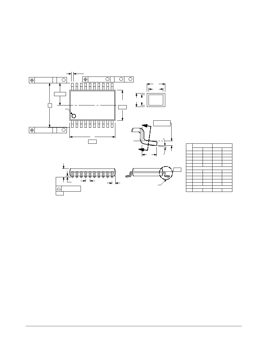
NCN6001
http://onsemi.com
35
PACKAGE DIMENSIONS
TSSOP - 20
DTB SUFFIX
CASE 948E - 02
ISSUE B
DIM
A
MIN
MAX
MIN
MAX
INCHES
6.60
0.260
MILLIMETERS
B
4.30
4.50
0.169
0.177
C
1.20
0.047
D
0.05
0.15
0.002
0.006
F
0.50
0.75
0.020
0.030
G
0.65 BSC
0.026 BSC
H
0.27
0.37
0.011
0.015
J
0.09
0.20
0.004
0.008
J1
0.09
0.16
0.004
0.006
K
0.19
0.30
0.007
0.012
K1
0.19
0.25
0.007
0.010
L
6.40 BSC
0.252 BSC
M
0 8 0 8
_
_
_
_
NOTES:
1. DIMENSIONING AND TOLERANCING PER
ANSI Y14.5M, 1982.
2. CONTROLLING DIMENSION: MILLIMETER.
3. DIMENSION A DOES NOT INCLUDE MOLD
FLASH, PROTRUSIONS OR GATE BURRS.
MOLD FLASH OR GATE BURRS SHALL
NOT EXCEED 0.15 (0.006) PER SIDE.
4. DIMENSION B DOES NOT INCLUDE
INTERLEAD FLASH OR PROTRUSION.
INTERLEAD FLASH OR PROTRUSION
SHALL NOT EXCEED 0.25 (0.010) PER
SIDE.
5. DIMENSION K DOES NOT INCLUDE
DAMBAR PROTRUSION. ALLOWABLE
DAMBAR PROTRUSION SHALL BE 0.08
(0.003) TOTAL IN EXCESS OF THE K
DIMENSION AT MAXIMUM MATERIAL
CONDITION.
6. TERMINAL NUMBERS ARE SHOWN FOR
REFERENCE ONLY.
7. DIMENSION A AND B ARE TO BE
DETERMINED AT DATUM PLANE - W - .
ÕÕÕÕ
ÕÕÕÕ
ÕÕÕÕ
1
10
11
20
PIN 1
IDENT
A
B
- T -
0.100 (0.004)
C
D
G
H
SECTION N - N
K
K1
J J1
N
N
M
F
- W -
SEATING
PLANE
- V -
- U -
S
U
M
0.10 (0.004)
V
S
T
20X REF
K
L
L/2
2X
S
U
0.15 (0.006) T
DETAIL E
0.25 (0.010)
DETAIL E
6.40
0.252
---
---
S
U
0.15 (0.006) T

NCN6001
http://onsemi.com
36
ON Semiconductor and are registered trademarks of Semiconductor Components Industries, LLC (SCILLC). SCILLC reserves the right to make
changes without further notice to any products herein. SCILLC makes no warranty, representation or guarantee regarding the suitability of its products for any
particular purpose, nor does SCILLC assume any liability arising out of the application or use of any product or circuit, and specifically disclaims any and all
liability, including without limitation special, consequential or incidental damages. "Typical" parameters which may be provided in SCILLC data sheets and/or
specifications can and do vary in different applications and actual performance may vary over time. All operating parameters, including "Typicals" must be
validated for each customer application by customer's technical experts. SCILLC does not convey any license under its patent rights nor the rights of others.
SCILLC products are not designed, intended, or authorized for use as components in systems intended for surgical implant into the body, or other applications
intended to support or sustain life, or for any other application in which the failure of the SCILLC product could create a situation where personal injury or death
may occur. Should Buyer purchase or use SCILLC products for any such unintended or unauthorized application, Buyer shall indemnify and hold SCILLC
and its officers, employees, subsidiaries, affiliates, and distributors harmless against all claims, costs, damages, and expenses, and reasonable attorney fees
arising out of, directly or indirectly, any claim of personal injury or death associated with such unintended or unauthorized use, even if such claim alleges that
SCILLC was negligent regarding the design or manufacture of the part. SCILLC is an Equal Opportunity/Affirmative Action Employer.
PUBLICATION ORDERING INFORMATION
JAPAN: ON Semiconductor, Japan Customer Focus Center
2 - 9 - 1 Kamimeguro, Meguro - ku, Tokyo, Japan 153 - 0051
Phone: 81 - 3 - 5773- 3850
ON Semiconductor Website: http://onsemi.com
For additional information, please contact your local
Sales Representative.
NCN6001/D
Literature Fulfillment:
Literature Distribution Center for ON Semiconductor
P.O. Box 5163, Denver, Colorado 80217 USA
Phone: 303 - 675- 2175 or 800 - 344- 3860 Toll Free USA/Canada
Fax: 303 - 675- 2176 or 800 - 344- 3867 Toll Free USA/Canada
Email: orderlit@onsemi.com
N. American Technical Support: 800 - 282- 9855 Toll Free USA/Canada