
©
Semiconductor Components Industries, LLC, 2003
June, 2003 - Rev. 2
1
Publication Order Number:
NCN6004A/D
NCN6004A
Dual SAM/SIM Interface
Integrated Circuit
The NCN6004A is an interface IC dedicated for Secured Access
Module reader/writer applications. It allows the management of two
external ISO/EMV cards thanks to a simple and flexible
microcontroller interface. Several NCN6004A interfaces can share a
single data bus, assuming the external MPU provides the right Chip
Select signals to identify each IC connected on the bus. A built in
accurate protection system guarantees timely and controlled shutdown
in the case of external error conditions.
On top of that, the NCN6004A can independently handle the power
supply, in the range 2.7 V to 5.0 V input voltage, provided to each
external Smart Card. The interface monitors the current flowing into
each Smart Card, a flag being set in the case of overload.
Features
∑
Separated, Built-in DC/DC Converters Supply V
CC
Power to
External Cards
∑
100% Compatible with ISO 7816-3, EMV and GIE-CB Standards
∑
Fully GSM Compliant
∑
Individually Programmable ISO/EMV Clock Generator
∑
Built-in Programmable CRD_CLK Stop Function Handles Run or
High/Low State
∑
Programmable CRD_CLK Slopes to Cope with Wide Operating
Frequency Range
∑
Programmable Independent V
CC
Supply for Each Smart Card
∑
Support up to 65 mA V
CC
Supply to Each ISO/EMV Card
∑
Multiple NCN6004A Parallel Operation on a Shared Bus
∑
8 kV/Human Model ESD Protection on Each Interface Pin
∑
Provides C4/C8 Channels
∑
Provides 1.80 V, 3.0 V or 5.0 V Card Supply Voltages
Typical Applications
∑
Set Top Box Decoder
∑
ATM Multi Systems, POS, Handheld Terminals
∑
Internet E-commerce PC Interface
∑
Multiple Self Serve Automatic Machines
∑
Wireless Phone Payment Interface
∑
Automotive Operating Time Controller
http://onsemi.com
MARKING
DIAGRAM
Device
Package
Shipping
ORDERING INFORMATION
NCN6004AFTBR2
TQFP48
2000 Tape & Reel
TQFP48
CASE 932F
PLASTIC
NCN6004A
AWLYYWW
A
= Assembly Location
WL = Wafer Lot
YY = Year
WW = Work Week
1
48

NCN6004A
http://onsemi.com
2
CRD_IO_A
CRD_RST_A
CRD_CLK_A
CRD_VCC_A
CRD_C4_A
CRD_C8_A
CRD_DET_A
CRD_IO_B
CRD_RST_
B
CRD_CLK_B
CRD_VCC_B
CRD_C8_B
CRD_C4_B
CRD_DET_
B
PWR_ON
ST
A
TUS
A0
A1
RESET_A
I/O_A
CLOCK_IN_A
C4_A
C8_A
PWR_VCC_A
PWR_GND
L1b
L2b
L2a
L1a
ANLG_GND
A2
ANLG_VCC
PWR_VCC_B
A3
1
2
3
4
5
6
7
8
9
10
11
12
13
14
15
16
17
18
19
20
21
22
23
24
25
26
27
28
29
30
31
32
33
34
35
36
37
38
39
40
41
42
43
44
CARD_SEL
EN_RPU
I/O_B
RESET_B
CLOCK_IN_B
C4_B
C8_B
45
46
47
48
ANLG_GND
PWR_GND
ANLG_GND
MUX_MODE
PGM
CS
INT
Figure 1. Pin Diagram
8
7
6
5
8
7
6
5
GND
GND
DA
T
A
POR
T#A
DA
T
A
POR
T#B
MPU BUS
MICRO CONTROLLER
7
PWR_ON
8
STATUS
A0
1
A1
2
CARD_SEL
5
6
I/O_A
9
RESET_A
10
C4_A
11
C8_A
12
CLK_IN_A
13
A2
3
A3
4
EN_RPU
MUX_MODE
47
ANLG_GND
14
ANLG_GND
48
ANLG_VCC
42
ANLG_GND
43
CLK_IN_B
15
C8_B
16
C4_B
17
RESET_B
18
I/O_B
19
C3
10
m
F
C1
10
m
F
V
CC
V
CC
DET
17
1
RST
2
CLK
3
C4
4
C8
I/O
VPP
GND
DET
18
J1
SMARTCARD # A
DET
17
1
2
3
4
DET
18
J2
SMARTCARD # B
GND
GND
GND
GND
PWR_VCC_A
28
PWR_GND
36
CRD_DET_A
20
CRD_VCC_A
29
CRD_CLK_A
30
CRD_IO_A
24
CRD_DET_B
41
CRD_VCC_B
32
CRD_CLK_B
31
CRD_IO_B
37
CRD_RST_A
23
CRD_RST_B
38
CRD_C4_A
22
CRD_C8_A
21
CRD_C4_B
39
CRD_C8_B
40
PWR_VCC_B
33
PWR_GND
25
GND
V
CC
V
CC
PGM
CS
INT
100 nF
L1
L1a
L2a
L2b
L1b
Figure 2. Typical Application
V
CC
RST
CLK
C4
C8
I/O
VPP
GND
C4
22
m
H
L2
22
m
H
35
34
26
27
46
44
45
CHIP SELECT
IRQ
C2
10
m
F
GND
NCN6004A

NCN6004A
http://onsemi.com
3
35
36
31
30
20
41
24
37
23
38
29
34
25
L1b
L2b
32
CARD#A DETECTION
CARD#B DETECTION
I/O#A
I/O#B
CLK#A
CLK#B
CLK#A
CLK#B
DET#B
GND
21
40
39
22
CRD_C4A
CRD_C8A
CRD_C8B
CRD_C4B
CRD_IOA
CRD_IOB
CRD_CLKA
PWR_GND
PWR_GND
CRD_VCCA
CRD_VCCB
CRD_CLKB
CRD_RSTA
CRD_RSTB
33
28
C4A
C8A
C4B
C8B
PWR_VCCA
PWR_VCCB
CRD_DETB
CRD_DETA
RESET_A
CLK_A
CLK_B
GND
Figure 3. Block Diagram
13
7
47
8
1
15
100 k
INPUT VOLTAGE
42
6
ANLG_VCC
PWR_ON
A0
A1
CLK_INA
CLK_INB
AGND
43
A2
A3
2
3
5
CARD_SEL
GND
INT
CS
PGM
MONITOR
V
CC
V
CC
IO_A
RST_A
C4A
C8A
IO_B
RST_B
C4B
C8B
CNTL
CNTL
4
27
9
10
26
50 k
16
DC/DC CONVER
TER
CARD #A
DC/DC CONVER
TER
PINS DRIVERS
PINS DRIVERS
CARD#A
CARD#B
CARD#B
CARD#A
SEQUENCER
CARD#B SEQUENCER
INTERRUPT BLOCK
CLOCK#A
CLOCK#B
DIGIT
AL
BLOCK
DET#B
DET#A
17
12
45
11
I/O_A
I/O_B
C4A
C8A
18
19
C4B
C8B
RESET_A
EN_RPU
MUX_MODE
44
26 k
100 k
RESET_B
DIVIDER
DIVIDER
IO_A
C4A
C8A
IO_B
C4B
C8B
CONTROL
ANALOG & DIGIT
AL
MUL
TIPLEX
100 k
100 k
26 k
100 k
100 k
100 k
RST_A
RST_B
NOTE:
An internal active pull down device forces all the
smart card pins to zero when the chip is deactivated.
DET#A
RESET_A
L1a
L2a
46
STATUS
V
CC
50 k

NCN6004A
http://onsemi.com
4
PIN DESCRIPTION
Pin
Symbol
Type
Description
1
A0
INPUT
This pin is combined with CS, A1, A2, A3, CARD_SEL and PGM to program the chip
mode of operation, the CRD_VCC voltage value, and to read the data provided by
the internal STATUS register (Table 1).
2
A1
INPUT
This pin is combined with CS, A0, A2, A3, CARD_SEL and PGM to program the chip
mode of operation, the CRD_VCC voltage value, and to read the data provided by
the internal STATUS register (Table 1).
3
A2
INPUT
This pin is combined with CS, A0, A1, A3, CARD_SEL and PGM to program the chip
mode of operation, the CRD_VCC voltage value, and to read the data provided by
the internal STATUS register (Table 1).
4
A3
INPUT
This pin is combined with CS, A0, A1, A2, CARD_SEL and PGM to program the chip
mode of operation, the CRD_VCC voltage value, and to read the data provided by
the internal STATUS register (Table 1).
5
CARD_SEL
INPUT
This pin provides logic identification of the Card #A/Card #B external smart card.
The logic signal is set up by the external microcontroller.
CARD_SEL = High
selection of the Smart Card A connected to pins 20, 21, 22,
23, 24, 29 and 30 (respectively CRD_DET_A, CRD_C8_A, CRD_C4_A,
CRD_RST_A, CRD_IO_A, CRD_VCC_A and CRD_CLK_A).
CARD_SEL = Low
selection of the Smart Card B connected to pins 41, 39, 40,
31, 38, 37, and 32 (respectively CRD_DET_B, CRD_C4_B, CRD_C8_B,
CRD_CLK_B, CRD_RST_B, CRD_IO_B, and CRD_VCC_B).
¡¡¡
¡
¡
¡
¡
¡
¡
¡
¡
¡
¡
¡
¡
¡
¡
¡
¡¡¡
6
¡¡¡¡¡¡
¡
¡¡¡¡
¡
¡
¡¡¡¡
¡
¡
¡¡¡¡
¡
¡
¡¡¡¡
¡
¡
¡¡¡¡
¡
¡¡¡¡¡¡
PGM
¡¡¡¡¡¡
¡
¡¡¡¡
¡
¡
¡¡¡¡
¡
¡
¡¡¡¡
¡
¡
¡¡¡¡
¡
¡
¡¡¡¡
¡
¡¡¡¡¡¡
DIGITAL INPUT
¡¡¡¡¡¡¡¡¡¡¡¡¡¡¡¡¡¡¡¡¡
¡
¡¡¡¡¡¡¡¡¡¡¡¡¡¡¡¡¡¡¡
¡
¡
¡¡¡¡¡¡¡¡¡¡¡¡¡¡¡¡¡¡¡
¡
¡
¡¡¡¡¡¡¡¡¡¡¡¡¡¡¡¡¡¡¡
¡
¡
¡¡¡¡¡¡¡¡¡¡¡¡¡¡¡¡¡¡¡
¡
¡
¡¡¡¡¡¡¡¡¡¡¡¡¡¡¡¡¡¡¡
¡
¡¡¡¡¡¡¡¡¡¡¡¡¡¡¡¡¡¡¡¡¡
This pin is combined with CS, A0, A1, A2, A3, and CARD_SEL to program the chip
mode of operation and to read the data provided by the internal STATUS register
(Figure 4 and Table 1).
PGM = H
the NCN6004A is under normal operation and all the data with the exter-
nal card can be exchanged using any of the Smart Card A or Smart Card B Lines
PGM = Low
the NCN6004A runs the programming mode and related parameters
can be re programmed according to a given need. In this case, the related card side
logic signals are latched in their previous states and no transaction can occurs.
The programmed states are latched upon the PGM rising slope (Figure 4).
¡¡¡
¡
¡
¡
¡
¡
¡
¡
¡
¡
¡
¡
¡
¡
¡
¡
¡¡¡
7
¡¡¡¡¡¡
¡
¡¡¡¡
¡
¡
¡¡¡¡
¡
¡
¡¡¡¡
¡
¡
¡¡¡¡
¡
¡
¡¡¡¡
¡
¡¡¡¡¡¡
CS
¡¡¡¡¡¡
¡
¡¡¡¡
¡
¡
¡¡¡¡
¡
¡
¡¡¡¡
¡
¡
¡¡¡¡
¡
¡
¡¡¡¡
¡
¡¡¡¡¡¡
DIGITAL INPUT
¡¡¡¡¡¡¡¡¡¡¡¡¡¡¡¡¡¡¡¡¡
¡
¡¡¡¡¡¡¡¡¡¡¡¡¡¡¡¡¡¡¡
¡
¡
¡¡¡¡¡¡¡¡¡¡¡¡¡¡¡¡¡¡¡
¡
¡
¡¡¡¡¡¡¡¡¡¡¡¡¡¡¡¡¡¡¡
¡
¡
¡¡¡¡¡¡¡¡¡¡¡¡¡¡¡¡¡¡¡
¡
¡
¡¡¡¡¡¡¡¡¡¡¡¡¡¡¡¡¡¡¡
¡
¡¡¡¡¡¡¡¡¡¡¡¡¡¡¡¡¡¡¡¡¡
This pin provides the Chip Select Function for the NCN6004A device.
CS = High
Pins A0, A1, A2, A3, CARD_SEL, PGM, PWR_ON, RESET_A, RE-
SET_B, C4_A, C4_B, C8_A, C8_B, I/O_A and I/O_B are disabled, the pre activated
CRD_VCC maintains it's currently programmed value.
CS = Low
Pins A0, A1, A2, A3, CARD_SEL, PGM, PWR_ON, RESET_A, RE-
SET_B, C4_A, C4_B, C8_A, C8_B, I/O_A and I/O_B are activated, all the functions
being available.An internal pull up resistor, connected to V
CC
, provides a logic bias
when the external
m
P is in the high impedance state.
8
PWR_ON
DIGITAL INPUT
This pin activates or deactivates the DC/DC converter selected by CARD_SEL upon
positive/negative going transient.
PWR_ON = Positive going High
DC/DC Activated
PWR_ON = Negative going L
DC/DC switched Off, no power is applied to the
associated output CRD_VCC pin.
Since uncontrolled action could take place during the rise voltage of the related
CRD_VCC_x output, care must be observed to avoid a PWR_ON negative going
transient during this period of time. To avoid any logical latch up, using a minimum
1.0 ms delay is recommended prior to power down the related DC/DC converter
following a power up command (Figure 12).
9
I/O_A
INPUT/OUTPUT
This pin carries the data transmission between an external microcontroller and the
external smart card #A.
A built-in bi-directional level translator adapts the signal flowing between the card
and the MCU. The level translator is enabled when CS = Low. Since a dedicated line
is used to communicate the data between the MPU and the smart card, the user can
activate the two channels simultaneously, assuming the
m
P provides a pair of I/O
lines.
When MUX_MODE = High, this pin provides an access to either card A or B I/O by
means of CARD_SEL selection bit. On the other hand, the internal pull up resistor is
automatically disconnected when MUX_MODE = High, avoiding a current overload
on the I/O line, regardless of the EN_RPU logic level.
This pull up resistor is under the EN_RPU control when MUX_MODE = Low.

NCN6004A
http://onsemi.com
5
PIN DESCRIPTION (continued)
Pin
Description
Type
Symbol
10
RESET_A
INPUT
The signal present on this pin is translated to the RST pin of the external smart card
#A. The CS signal must be Low to validate the RESET function, regardless of the
selected card.
Assuming the
m
P provides two independent lines to control the RESET pins, the
NCN6004A can control two cards simultaneously.
When MUX_MODE = High, this pin provides an access to either card A or B Reset
by means of CARD_SEL selection bit.
The associated pull up resistor is either connected to V
CC
(EN_RPU = H) or discon-
nected when EN_RPU = Low.
11
C4_A
INPUT
This pin controls the card #A C4 contact The signal can be either de-multiplexed, at
MPU level, or is multiplexed with C4_B, depending upon the MUX_MODE logic
state.
When MUX_MODE = High, this pin provides an access to either card A or B C4
channel by means of CARD_SEL selection bit.
The associated pull up resistor is either connected to V
CC
(EN_RPU = H) or discon-
nected when EN_RPU = Low.
12
C8_A
INPUT
This pin controls the card #A C8 contact. The signal can be either de-multiplexed, at
MPU level, or is multiplexed with C8_B, depending upon the MUX_MODE logic
state.
When MUX_MODE = High, this pin provides an access to either card A or B C8
channel by means of CARD_SEL selection bit.
The associated pull up resistor is either connected to V
CC
(EN_RPU = H) or discon-
nected when EN_RPU = Low.
13
CLOCK_IN_A
Clock Input,
High Impedance
The signal present on this pin comes from either the MCU master clock, or from any
signal fulfilling the logic level and frequency specifications. This signal is fed to the
internal clock selection circuit prior to be connected to the external smart card #A.
Each of the external card can have different division ratio, depending upon the state
of the CRD_SEL pin and associated programming bits. The built-in circuit can be
programmed to 1/1, 1/2, 1/4 or 1/8 frequency division ratio.
This input is valid and routed to either CRD_CLK_A _DIVIDER or CRD_CLK_B_DI-
VIDER regardless of the MUX_MODE state, depending upon the CLK_D_A/
CRD_D_B and CARD_SEL programmed states (Table 1).
Although this input supports the signal coming from a crystal oscillator, care must be
observed to avoid digital levels outside the specified V
IH
/V
IL
range. Similarly, the
input clock signal shall have rise and fall times compatible with the operating fre-
quency.
14
ANLG_GND
POWER
This pin is the ground reference for both analog and digital signals and must be con-
nected to the system Ground. Care must be observed to provide a copper PCB lay-
out designed to avoid small signals and power transients sharing the same track.
Good high frequency techniques are strongly recommended.
15
CLOCK_IN_B
Clock Input,
High Impedance
The signal present on this pin comes from either the MCU master clock, or from any
signal fulfilling the logic level and frequency specifications. This signal is fed to the
internal clock selection circuit prior to be connected to the external smart card #B.
Each of the external card can have different division ratio, depending upon the state
of the CRD_SEL pin and associated programming bits. The built-in circuit can be
programmed to 1/1, 1/2, 1/4, or 1/8 frequency division ratio.
This input is valid and routed to either CRD_CLK_B_DIVIDER or CRD_CLK_A_DI-
VIDER regardless of the MUX_MODE state, depending upon the
CRD_D_B/CRD_D_A and CARD_SEL programmed states (Table 1).
Although this input supports the signal coming from a crystal oscillator, care must be
observed to avoid digital levels outside the specified V
IH
/V
IL
range. Similarly, the
input clock signal shall have rise and fall times compatible with the operating fre-
quency.
16
C8_B
INPUT
This pin controls the card #B C8 contact. The signal can be either de -multiplexed,
at MPU level, or is multiplexed with C8_A, depending upon the MUX_MODE logic
state.
When MUX_MODE = High, this pin is internally disable, a pull up resistor is con-
nected to V
CC
(regardless of the logic state of EN_RPU is), and the access to card B
takes place by C8_A associated with CARD_SEL selection bit.
The associated pull up resistor is either connected to V
CC
(EN_RPU = H) or discon-
nected when EN_RPU = Low.

NCN6004A
http://onsemi.com
6
PIN DESCRIPTION (continued)
Pin
Description
Type
Symbol
17
C4_B
INPUT
This pin controls the card #B C4 contact. The signal can be either de -multiplexed,
at MPU level, or is multiplexed with C8_A, depending upon the MUX_MODE logic
state.
When MUX_MODE = High, this pin is internally disable, a pull up resistor is con-
nected to V
CC
, (regardless of the logic state of EN_RPU), and the access to card B
takes place by C4_A associated with CARD_SEL selection bit.
The associated pull up resistor is either connected to V
CC
(EN_RPU = H) or discon-
nected when EN_RPU = Low.
18
RESET_B
INPUT
The signal present on this pin is translated to the RST pin of the external smart card
#B. The CS signal must be Low to valid the RESET function, regardless of the se-
lected card. Assuming the
m
P provides two independent lines to control the RESET
pins, and MUX_MODE = Low, the NCN6004A can control two cards simultaneously.
When MUX_MODE = High, this pin is internally disable, a pull up resistor is con-
nected to V
CC
, (regardless of the logic state of EN_RPU), and the access to card B
takes place by RESET_A associated with CARD_SEL selection bit.
The associated pull up resistor is either connected to V
CC
(EN_RPU = H) or discon-
nected when EN_RPU = Low.
19
I/O_B
INPUT/OUTPUT
This pin carries the data transmission between an external microcontroller and the
external smart card #B.
A built-in bi-directional level translator adapts the signal flowing between the card
and the MCU. The level translator is enabled when CS = Low. The signal present on
this pin is latched when CS = High. Since a dedicated line is used to communicate
the data between the
m
P and the smart card, (assuming MUX_MODE = Low) the
user can activate the two channels simultaneously, assuming the
m
P provides a pair
of I/O lines. When MUX_MODE = High, this pin is internally disable, the pull up re-
sistor is connected to V
CC
, (regardless of the logic state of EN_RPU), and the ac-
cess to card B takes place by I/O_A associated with CARD_SEL selection bit.
20
CRD_DET_A
INPUT
This pin senses the signal coming from the external smart card connector to detect
the presence of card #A. The polarity of the signal is programmable as Normally
Open or Normally Close switch. The logic signal will be activated when the level is
either Low or High, with respect to the polarity defined previously. By default, the
input is Normally Open. A built-in circuit prevents uncontrolled short pulses to gen-
erate an INT signal. The digital filter eliminates pulse width below 50
m
s (see spec).
21
CRD_C8_A
OUTPUT
This pin controls the card #A C8 contact, according to the ISO7816 specifications. A
built-in level shifter is used to adapt the card and the
m
C, regardless of the power
supply voltage of each signals.
The signal present at this pin is latched upon either CARD_SEL =L, or CS = H or
PGM = L, and resume to a transparent mode when card #A is selected and operates
in the transfer mode.The pin is hardwired to zero, the bias being provided by the
V
CC
supply, when either the V
CC
voltage drops below 2.7 V, or during the
CRD_VCC_A start-up time.
22
CRD_C4_A
OUTPUT
This pin controls the card #A C4 contact, according to the ISO7816 specifications. A
built-in level shifter is used to adapt the card and the MCU, regardless of the power
supply voltage of each signals.
The signal present at this pin is latched upon either CARD_SEL = L, or CS = H, or
PGM = L, and resume to a transparent mode when card #A is selected and operates
in the transfer mode.
The pin is hardwired to zero, the bias being provided by the V
CC
supply, when either
the V
CC
voltage drops below 2.7 V, or during the CRD_VCC_A start-up time.
23
CRD_RST_A
OUTPUT
This pin is connected to the external smart card #A to support the RESET signal. A
built-in level shifter is used to adapt the card and the MCU, regardless of the power
supply voltage of each signals.
The signal present at this pin is latched upon either CARD_SEL = Low, or when CS
or PGM returns to a High, and resume to a transparent mode when card #A is se-
lected. The pin is hardwired to zero, the bias being provided by the V
CC
supply,
when either the V
CC
voltage drops below 2.7 V, or during the CRD_VCC_A start-up
time.

NCN6004A
http://onsemi.com
7
PIN DESCRIPTION (continued)
Pin
Description
Type
Symbol
24
CRD_IO_A
INPUT/OUTPUT
This pin carries the data serial connection between the external smart card #A and
the microcontroller. A built-in bidirectional level shifter is used to adapt the card and
the MCU, regardless of the power supply voltage of each signals.
This pin is biased by a pull up resistor connected to CRD_VCC_A. When CS = High,
the CRD_IO_A holds the previous I/O logic state and resume to a normal operation
when this pin is reactivated.
The pin is hardwired to zero, the bias being provided by the V
CC
supply, when either
the V
CC
voltage drops below 2.7 V, or during the CRD_VCC_A start-up time.
25
PWR_GND
POWER
This pin carries the power current flow coming from the built in DC/DC converters. It
is associated with the external card # A. It must be connected to the system Ground
and care must be observed at PCB layout level to avoid the risk of spike voltages on
the logic lines.
26
L2_A
POWER
Connects one side of the external DC/DC converter inductor #A (Note 1)
27
L1_A
POWER
Connects one side of the external DC/DC converter inductor #A (Note 1).
28
PWR_VCC_A
POWER
This pin is connected to the positive external power supply. The device sustains any
voltage from +2.7 V to +5.5 V. This voltage supplies the NCN6004A internal circuits
and is regulated by the internal DC/DC converter to provide the DC voltage to the
external card. A high quality capacitor must be connected across pin 28 and
PWR_GND, 10
m
F/6.0 V ceramic X7R or X5R type is recommended.
Note: The voltage present at pin 28 and 33 must be equal to the voltage present at
pin 42.
29
CRD_VCC_A
POWER
This pin provides the power supply to the external smart card #A. The V
CC
voltage is
defined by programming the NCN6004A accordingly. Since the cards have indepen-
dent DC/DC converter, the output voltage can have any value independently from
CARD_B.
A high quality, low ESR capacitor is mandatory to achieve the V
CC
specifications.
Using two 4.7
m
F/6.0 V ceramic X7R or X5R capacitors in parallel is recommended.
30
CRD_CLK_A
OUTPUT
This pin is connected to the CLK external smart card #A pin. The signal comes from
the built- in frequency divider dedicated to the #A card. The clock is selected and con-
trolled by setting the logic inputs according to Table 1. The slope of the output clock can
be selected between one of the two programmable mode: SLOW or FAST (Table 8).
The pin is hardwired to zero, the bias being provided by the V
CC
supply, when either
the V
CC
voltage drops below 2.7 V, or during the CRD_VCC_A start- up time.
31
CRD_CLK_B
OUTPUT
This pin is connected to the CLK external smart card #B pin. The signal comes from
the built- in frequency divider dedicated to the #B card. The clock is selected and con-
trolled by setting the logic inputs according to Table 1. The slope of the output clock can
be selected between one of the two programmable mode: SLOW or FAST (Table 8).
The pin is hardwired to zero, the bias being provided by the V
CC
supply, when either
the V
CC
voltage drops below 2.7 V, or during the CRD_VCC_B start- up time.
32
CRD_VCC_B
POWER
This pin provides the power supply to the external smart card #B. The V
CC
voltage is
defined by programming the NCN6004A accordingly. Since the cards have indepen-
dent DC/DC converter, the output voltage can have any value independently from
CARD_A.
A high quality, low ESR capacitor is mandatory to achieve the V
CC
specifications.
Using two 4.7
m
F/6.0 V ceramic X7R or X5R capacitors in parallel is recommended.
33
PWR_VCC_B
POWER
This pin is connected to the positive external power supply. The device sustains any
voltage from +2.7 V to +6.0 V. This voltage supplies the NCN6004A internal circuits
and is regulated by the internal DC/DC converter to provide the DC voltage to the
external card. A high quality capacitor must be connected across pin 33 and
PWR_GND, 10
m
F/6.0 V ceramic X7R type is recommended.
Note: The voltage present on pin 28 and 33 must be equal to the voltage present on
pin 42
34
L2b
POWER
Connects one side of the external DC/DC converter inductor #B (Note 1).
35
L1b
POWER
Connects one side of the external DC/DC converter inductor #B (Note 1).
36
PWR_GND
POWER
This pin carries the power current flow coming from the built in DC/DC converters. It
is associated with the external card # B. It must be connected to the system Ground
and care must be observed at PCB layout level to avoid the risk of spike voltages on
the logic lines.
¡¡¡¡¡¡¡¡¡¡¡¡¡¡¡¡¡¡¡¡¡¡¡¡¡¡¡¡¡¡¡¡¡
¡
¡¡¡¡¡¡¡¡¡¡¡¡¡¡¡¡¡¡¡¡¡¡¡¡¡¡¡¡¡¡¡
¡
¡¡¡¡¡¡¡¡¡¡¡¡¡¡¡¡¡¡¡¡¡¡¡¡¡¡¡¡¡¡¡¡¡
1. The external inductors shall preferably have the same values. Depending upon the power absorbed by the load, the inductor can range
from 10
m
H to 47
m
H. To achieve the highest yield, the inductor shall have an ESR < 1.0
W
.

NCN6004A
http://onsemi.com
8
PIN DESCRIPTION (continued)
Pin
Description
Type
Symbol
37
CRD_IO_B
INPUT/OUTPUT
This pin carries the data serial connection between the external smart card #B and
the microcontroller. A built-in bi-directional level shifter is used to adapt the card
and the MCU, regardless of the power supply voltage of each signals.
This pin is biased by a pull up resistor connected to CRD_VCC_A. When CS = High,
the CRD_IO_A holds the previous I/O logic state and resume to a normal operation
when this pin is reactivated.
The pin is hardwired to zero, the bias being provided by the V
CC
supply, when either
the V
CC
voltage drops below 2.7 V, or during the CRD_VCC_B start-up time.
38
CRD_RST_B
OUTPUT
This pin is connected to the external smart card #B to support the RESET signal. A
built-in level shifter is used to adapt the card and the MCU, regardless of the power
supply voltage of each signals.
The signal present at this pin is latched upon either CARD_SEL or CS or PGM posi-
tive going transient and resume to a transparent mode when card #B is selected.
The pin is hardwired to zero, the bias being provided by the V
CC
supply, when either
the V
CC
voltage drops below 2.7 V, or during the CRD_VCC_B start-up time.
39
CRD_C4_B
OUTPUT
This pin controls the card #B C4 contact, according to the ISO specification. A built-
in level shifter is used to adapt the card and the MCU, regardless of the power sup-
ply voltage of each signals. The signal present at this pin is latched upon either
CARD_SEL or CS or PGM
positive going transient and resume to a transparent
mode when card #B is selected.
The pin is hardwired to zero, the bias being provided by the V
CC
supply, when either
the V
CC
voltage drops below 2.7 V, or during the CRD_VCC_B start-up time.
40
CRD_C8_B
OUTPUT
This pin controls the card #B C8 contact, according to the ISO specification. A built-
in level shifter is used to adapt the card and the MCU, regardless of the power sup-
ply voltage of each signals. The signal present at this pin is latched upon either
CARD_SEL or CS or PGM positive going transient and resume to a transparent
mode when card #B is selected.
The pin is hardwired to zero, the bias being provided by the V
CC
supply, when either
the V
CC
voltage drops below 2.7 V, or during the CRD_VCC_B start-up time.
41
CRD_DET_B
INPUT
This pin senses the signal coming from the external smart card connector to detect
the presence of card #B. The polarity of the signal is programmable as Normally
Open or Normally Close switch. The logic signal will be activated when the level is
either Low or High, with respect to the polarity defined previously. By default, the
input is Normally Open. A built-in circuit prevents uncontrolled short pulses to gen-
erate an INT signal. The digital filter eliminates pulse width below 50
m
s.
42
ANLG_VCC
POWER
This pin is connected to the positive external power supply. The device sustains any
voltage from +2.7 V to +5.5 V. This voltage supplies the NCN6004A internal Analog
and Logic circuits. A high quality capacitor must be connected across this pin and
ANLG_GND, 10
m
F/6 V is recommended. A set of extra pins (28 and 33) are pro-
vided to connect the power supply to the internal DC/DC converter.
Note: The voltage present at pin 28 and 33 must be equal to the voltage present at
pin 42
43
ANLG_GND
GROUND
This pin is the ground reference for both analog and digital signals and must be con-
nected to the system Ground. Care must be observed to provide a copper PCB lay-
out designed to avoid small signals and power transients sharing the same track.
Good high frequency techniques are strongly recommended.
44
MUX_MODE
INPUT
This pin selects the mode of operation of the card signals from the MPU side. When
MUX_MODE = Low, all the card signals are fully de-multiplexed and data transfers
can take place with both cards simultaneously. On top of that, both cards can be
accessed during the programming sequence, assuming the external microcontroller
is capable to run multi tasks software.
When MUX_MODE = High, all the card signals are multiplexed and the communica-
tions with the cards shall take place in a sequential mode. The card is selected by
setting CARD_SEL high or Low. The internal logic will disable the CARD_B inputs
and use CARD_SEL inputs as a single channel to controls both output smart cards
sequentially when MUX_MODE = H.
Moreover, when MUX_MODE = High, all the B channel
m
P dedicated pins, except
CLOCK_IN_B, pin 15, are forced to a high level by means of internal pull up resis-
tors. It is not necessary to connect these pins (16, 17, 18 and 19) to an external bias
voltage, but it is mandatory to avoid any connections to ground. On the other hand,
in this case the internal pull up resistor connected across I/O_A, pin 9 and V
CC
is
automatically disconnected to avoid a current overload on the I/O line.

NCN6004A
http://onsemi.com
9
PIN DESCRIPTION (continued)
Pin
Description
Type
Symbol
45
EN_RPU
INPUT
This pin provides a logic input to valid or not the internal pull up resistors connected
across each I/O, RESET, C4 and C8 lines and ANLG_VCC.
When EN_RPU = High, the pull up resistors are connected
When EN_RPU = Low, the pull up resistors are disconnected and it is up to the de-
signer to set up the external resistor to cope with the ISO/EMV specifications.
The logic signal must be set up prior to apply the ANLG_VCC supply. Once the logic
mode has been acknowledged by the internal Power On reset, it cannot be changed
until a new start-up sequence is launched.
46
STATUS
OUTPUT
This pin provides a logic state related to the card [A or B] insertion, the VCC_OK,
the CRD_VCC value and the current overflow powered to either card [A or B]. The
internal register can be read when PGM = High. The logic level is forced to High
when the input voltage drops below the V
bat
min (2.0 V), thus reducing the stand by
current, assuming the STATUS pin is not pulled down externally.
The associated pull up resistor is either connected to V
CC
(EN_RPU = H) or discon-
nected when EN_RPU = Low.
47
INT
OUTPUT
This pin is activated LOW when a card has been inserted and detected in either of
the external ports. The signal is reset by either a positive going transition on pin CS,
or by a High level on pin PWR_ON combined with CS = Low.
Similarly, an interrupt is generated when either one of the CRD_VCC output is over-
loaded.
On the other hand, the pin is forced to a logic High when the input voltage V
CC
drops below 2.0 V min.
The associated pull up resistor is either connected to V
CC
(EN_RPU = H) or discon-
nected when EN_RPU = Low.
48
ANLG_GND
GROUND
This pin is the ground reference for both analog and digital signals and must be con-
nected to the system Ground. Care must be observed to provide a copper PCB lay-
out designed to avoid small signals and power transients sharing the same track.
Good high frequency techniques are strongly recommended.
MAXIMUM RATINGS
(Note 2)
Rating
Symbol
Value
Unit
Power Supply Input Supply Voltage
V
CC
6
V
V
in
Digital Input Pins
-0.5 V < V
in
< V
CC
+0.5 V,
but < 6.0 V
V
Power Supply Input Current
IV
CC
500
mA
Digital Input Pins
V
in
In
-0.5 < V
CC
or V
CC
< 5.5
"
5
V
mA
Digital Output Pins
V
out
I
out
-0.5 < V
CC
or V
CC
< 5.5
"
10
V
mA
Card Interface Pins
V
card
I
card
-0.5V < V
card
< CRD_VCC +0.5V
15 mA (internally limited)
V
mA
ESD Capability, Human Body Model (Note 3)
Standard Pins
Card Interface Pins (Card A or B)
V
ESD
2
8
kV
kV
TQFP48
Power Dissipation @ Tab = +85
∞
C
Thermal Resistance Junction-to-Air
P
D
R
J
q
A
800
50
mW
∞
C/W
Operating Ambient Temperature Range
T
A
-40 to +85
∞
C
Operating Junction Temperature Range
T
J
-40 to +125
∞
C
Maximum Junction Temperature (Note 4)
T
Jmax
+150
∞
C
Storage Temperature Range
Tag
-65 to +150
∞
C
2. Maximum Electrical Ratings are defined as those values beyond which damage(s) to the device may occur at T
A
= +25
∞
C.
3. Human Body Model, R = 1500
W
, C = 100 pF.
4. Absolute Maximum Rating beyond which damage(s) to the device may occur.

NCN6004A
http://onsemi.com
10
POWER SUPPLY SECTION
General test conditions, unless otherwise specified: Operating temperature: -25
∞
C < T
A
< +85
∞
C,
V
CC
= +3.0 V, CRD_VCC_A = CRD_VCC_B = +5.0 V.
Rating
Symbol
Pin
Min
Typ
Max
Unit
I
out
= 2 x 65 mA (both external cards running simultaneously)
@ 3.0 V < V
CC
< 5.5 V
CRD_VCC
29, 32
4.6
-
5.4
V
I
out
= 2 x 55 mA per pin (both external cards running)
V
out
defined @ CRD_VCC = 3.0 V @ 3.0 V < V
CC
< 5.5 V
CRD_VCC
29, 32
2.7
-
3.3
V
I
out
= 2 x 35 mA per pin (both external cards running)
V
out
defined @ CRD_VCC = 1.80 V @ 3.0 V < V
CC
< 5.5 V
CRD_VCC
29, 32
1.65
-
1.95
V
Output Card Supply Voltage Ripple (per CRD_VCC outputs) @ :
L
out
= 22
m
H, L
ESR
< 2.0
W
, C
out
= 10
m
F per CRD_VCC (Note 5)
I
out
= 35 mA, V
out
= 1.80 V
I
out
= 55 mA, V
out
= 3.0 V
I
out
= 65 mA, V
out
= 5.0 V
V
ORA
V
ORB
29
32
-
-
-
-
-
-
50
50
50
mV
DC/DC Dynamic Inductor Peak Current @ V
bat
= 5.0 V, L
out
= 22
m
H,
C
out
= 10
m
F
CRD_VCC = 1.8 V
CRD_VCC = 3.0 V
CRD_VCC = 5.0 V
I
ccov
29, 32
-
-
-
200
280
430
-
-
-
mA
Standby Supply Current Conditions (Note 5):
ANLG_VCC = PWR_VCC = 3.0 V
PWR_ON = H, STATUS = H, CS = H
Card A and Card B CLOCK_IN = H, I/O = H, RESET = H
All Logic Inputs = H, Temperature range = 0
∞
C to +50
∞
C
ANLG_VCC = PWR_VCC = 5.0 V
Temperature range ≠25
∞
C to +85
∞
C
All other test conditions identical
ANLG_VCC = PWR_VCC = 1.8 V
Temperature range ≠25
∞
C to +50
∞
C
All other test conditions identical
Note: This parameter is guaranteed by design, not production tested.
I
DD
42, 28,
33
-
-
-
-
-
-
-
20
-
-
50
-
-
5.0
-
m
A
Operating Supply Current
ANLG_VCC = PWR_VCC
= 5.5 V
@ CRD_VCC_A/B = 5.0 V
@ CRD_VCC_ A/B = 3.0 V
@ CRD_VCC_ A/B = 1.85 V
ANLG_VCC = PWR_VCC = 3.3 V
@ CRD_VCC_A/B = 5.0 V
@ CRD_VCC_ A/B = 3.0 V
@ CRD_VCC_ A/B = 1.85 V
PWR_ON = H, CS = H, CLK_A = CLK_B = Low, all card pins unloaded
I
DDop
42, 28,
33
0.7
0.7
0.7
0.2
0.2
0.2
mA
V
bat
Under Voltage Detection Positive Going Slope
V
bat
Under Voltage Detection Negative Going Slope
V
bat
Under Voltage Detection Hysteresis
Note: The voltage present in pins 28 and 33 must be equal to or
Note:
lower than the voltage present in pin 42.
V
batLH
V
batLL
V
batHY
42
2.1
2.0
-
-
-
100
2.7
2.6
-
V
V
mV
Output Continuous Current Card A or Card B (both cards can be
operating simultaneously) @ 3.0 < V
CC
< 5.5 V
Output Voltage = 1.85 V
Output Voltage = 3.0 V
Output Voltage = 5.0 V
I
ccp
31, 42
35
55
65
mA
Output Over Current Limit (A or B)
V
bat
= 3.3 V, CRD_VCC = 1.8 V, 3.0 V or 5.0 V
V
bat
= 5.0 V, CRD_VCC = 1.8 V, 3.0 V or 5.0 V
I
ccov
31, 42
100
150
mA
Output Over Current Time Out Per Card
I
tdoff
31, 42
4.0
ms
Output Card Supply Turn On Time @
L
out
= 22
m
F, C
out
= 10
m
F Ceramic.
V
CC
= 2.7 V, CRD_VCC = 5.0 V (A or B)
V
CCTON
31, 42
500
m
s
5. Assuming ANLG_VCC and PWR_VCC pins are connected to the same power supply.

NCN6004A
http://onsemi.com
11
POWER SUPPLY SECTION
General test conditions, unless otherwise specified: Operating temperature: -25
∞
C < T
A
< +85
∞
C,
V
CC
= +3.0 V, CRD_VCC_A = CRD_VCC_B = +5.0 V. (continued)
Rating
Unit
Max
Typ
Min
Pin
Symbol
Output Card Supply Shut Off Time @
C
out
= 10
m
F, ceramic.
V
CC
= 2.7 V, CRD_VCC = 5.0 V, V
CCOFF
< 0.4 V (A or B)
V
CCTOFF
31, 42
100
250
m
s
DC/DC Converter Operating Frequency (A or B)
F
SW
31, 42
600
kHz
5. Assuming ANLG_VCC and PWR_VCC pins are connected to the same power supply.
DIGITAL INPUT/OUTPUT SECTION
2.70 < V
CC
< 5.50 V, Normal Operating Mode (-25
∞
C to +85
∞
C ambient temperature, unless otherwise noted)
Rating
Symbol
Pin
Min
Typ
Max
Unit
A0, A1, A2, A3, CARD_SEL, PWR_ON, PGM, CS, MUX_MODE,
EN_RPU, RESET_A, RESET_B, C4_A, C8_A, C4_B, C8_B
High Level Input Voltage
Low Level Input Voltage
Input Capacitance
V
IH
V
IL
C
in
1, 2, 3,
4, 5, 6,
7, 8,
44, 45,
10, 18,
11, 12,
16, 17
0.7 * V
bat
V
bat
0.3 * V
bat
10
V
V
pF
STATUS, INT
Output High Voltage @ I
OH
= -10
m
A
Output Low Voltage @ I
OH
= 200
m
A
V
OH
V
OL
46, 47
V
bat
≠1.0 V
0.40
V
STATUS, INT
Output Rise Time @ C
out
= 30 pF
Output Fall Time @ C
out
= 30 pF
trsta, trint
tfsta, tfint
5
100
m
s
ns
CLOCK_A Asynchronous Input Clock @ DC = 50%
"
1%
F
CLKINA
13
40
MHz
CLOCK_B Asynchronous Input Clock @ DC = 50%
"
1%
F
CLKINB
15
40
MHz
I/O_A, I/O_B, both directions @ C
out
= 30 pF
I/O Rise Time
I/O Fall Time
t
rioA
, t
rioB
t
fioA
, t
fioB
9, 19
0.8
0.8
m
s
STATUS Pull Up Resistance
R
STA
46
35
50
k
W
INT Pull Up Resistance
R
INT
47
35
50
k
W
I/O_A Pull Up Resistance
R
IOA
9
14
20
35
k
W
I/O_B Pull Up Resistance
R
IOB
19
14
20
35
k
W
RESET_A Pull Up Resistance
R
RSTA
10
60
100
k
W
RESET_B Pull Up Resistance
R
RSTB
18
60
100
k
W
C4_A Pull Up Resistance
R
C4A
11
60
100
k
W
C8_A Pull Up Resistance
R
C8A
12
60
100
k
W
C4_B Pull Up Resistance
R
C4B
17
60
100
k
W
C8_B Pull Up Resistance
R
C8B
16
60
100
k
W
CS Pull Up Resistance
R
CS
7
60
100
k
W
CRD_DET_A and CRD_DET_B Pull Up Resistance
R
DETA
R
DETB
20
41
500
500
k
W
k
W

NCN6004A
http://onsemi.com
12
CARD INTERFACE SECTION
@ 2.70 < V
CC
< 5.50 V, Normal Operating Mode (-25
∞
C to +85
∞
C ambient temperature, unless
otherwise noted) CRD_VCC_A = CRD_VCC_B = 1.8 V or 3.0 V or 5.0 V
Rating
Symbol
Pin
Min
Typ
Max
Unit
CRD_RST_A, CRD_RST_B Output Voltage
Output RST High Level @ Irst = -200
m
A
Output RST Low Level @ Irst = 200
m
A
CRD_RST_A, CRD_RST_B Rise and Fall time
RST Rise Time @ C
out
= 30 pF
RST Fall Time @ C
out
= 30 pF
V
OH
V
OL
trrst
tfrst
23, 38
23, 38
23, 38
23, 38
CRD_VCC-0.5
0
CRD_VCC
0.4
100
100
V
V
ns
ns
CRD_CLK_A, CRD_CLK_B Output Clock
Output Operating Clock Card A and Card B
Output Operating Clock DC, Card A and Card B
(Input DC = 50%,
"
1%)
Note: This parameter is guaranteed by design, functionality 100%
tested at production.
Output Operating Clock Rise Time SLOW Mode
Card A and Card B
Output Operating Clock Fall Time SLOW Mode
Card A and Card B
Output Operating Clock Rise Time FAST Mode
Card A and Card B
Output Operating Clock Fall Time FAST Mode
Card A and Card B
Output Clock High Level, Card A and Card B, @ Iclk = -200
m
A
Output Clock Low Level, Card A and Card B, @ Iclkc = 200
m
A
F
clkA
, F
clkB
trclka, trclkb
tfclka, tfclkb
trclka, trclkb
tfclka, tfclkb
V
OH
V
OL
30, 31
45
CRD_VCC-0.5
0
20
55
16
16
4
4
CRD_VCC
0.4
MHz
%
ns
ns
ns
ns
V
V
CRD_IO_A, CRD_IO_B Data Transfer
Data Transfer Frequency, Card A and Card B
Data Rise Time, Card A and Card B, @ C
out
= 30 pF
Data Fall Time, Card A and Card B, @ C
out
= 30 pF
Data Output High Level, Card A and Card B @ Icrd_io = -20
m
A
Data Output Low Level, Card A and Card B @ Icrd_io = 20
m
A
F
IOA
, F
IOB
t
rioa,
t
riob
t
fioa,
t
fiob
V
OH
V
OL
24, 37
CRD_VCC-0.5
0
400
0.8
0.8
CRD_VCC
0.4
kHz
m
s
m
s
V
V
CRD_IO_A and CRD_IO_B Output Voltages
I/O_A = I/O_B = 0, I
OL
= 500
m
A
V
OL
24, 37
0.40
V
CRD_C4_A, CRD_C4_B Output Voltages
Output C4 High Level @ Irst = -200
m
A
Output C4 Low Level @ Irst = 200
m
A
CRD_C4_A, CRD_C4_B Rise and Fall time
C4 Rise Time @ C
out
= 30 pF
C4 Fall Time @ C
out
= 30 pF
V
OH
V
OL
trc
4
tfc
4
22, 39
CRD_VCC-0.5
0
CRD_VCC
0.4
100
100
V
V
ns
ns
CRD_C8_A, CRD_C8_B Output Voltages
Output C4 High Level @ Irst = -200
m
A
Output C4 Low Level @ Irst = 200
m
A
CRD_C8_A, CRD_C8_B Rise and Fall Time
C8 Rise Time @ C
out
= 30 pF
C8 RST Fall Time @ C
out
= 30 pF
V
OH
V
OL
trc
8
tfc
8
21, 40
CRD_VCC-0.5
0
CRD_VCC
0.4
100
100
V
V
ns
Pull Up resistance, CS = Low, PWR_ON = High
CRD_IO_A
CRD_IO_B
R
OLA
R
OLB
24
37
14
14
20
20
35
35
k
W
Card Detection Bias Pull Up Current, Card A or Card B
CRD_DET_A, CRD_DET_B
I
DETA
I
DETB
20
41
15
15
m
A
Card Insertion/Extraction Negative Going Input Low Voltage
V
ILDETA
V
ILDETB
20
41
0
0
0.30 * V
bat
0.30 * V
bat
V
Card Detection Insertion/Extraction Digital Filtering Delay
CRD_DET_A
CRD_DET_B
t
dcina
t
dcinb
20
41
50
50
m
s
CARD_A or CARD_B short circuit current:
CRD_IO, CRD_RST, CRD_C4, CRD_C8
CRD_CLK
(According to ISO and EMV specifications)
Ishort
Ishortclk
15
70
mA

NCN6004A
http://onsemi.com
13
DIGITAL DYNAMIC SECTION NORMAL OPERATING MODE
Rating
Symbol
Pin
Min
Typ
Max
Unit
Card Signal Sequence Interval, CRD_VCC_A and CRD_VCC_B:
CRD_IO_A, CRD_RST_A, CRD_CLK_A, CRD_C4_A, CRD_C8_A
CRD_IO_B, CRD_RST_B, CRD_CLK_B, CRD_C4_B, CRD_C8_B
td
seq
24, 23,
30, 37,
38, 31
0.5
0.5
2
2
m
s
Internal RESET Delay
td
reset
1.0
m
s
Internal STATUS Delay Time
td
ready
46
1.0
m
s
PWR_ON Low State Pulse Width (Figure 11), Assuming CRD_VCC
reservoir capacitor = 10
m
F.
t
pwrlow
8
5
m
s
PWR_ON High State Pulse Width (Figure 11)
t
pwrset
8
200
ns
PWR_ON Preset Delay (Figure 11)
t
pwrpre
5, 7, 8
300
ns
PWR_ON Programming Hold Time (Figure 11)
t
pwrhold
5, 7, 8
100
ns
PWR_ON to CARD_SEL Change Delay Time (Figure 12)
t
cseldly
5, 6, 8
100
ns
PGM to PWR_ON Delay Time (Figure 12)
tpgmdly
5, 6, 8
300
ns
PWR_ON internal Set/Reset Pulses Width (Figure 12)
tpwrp
8
20
ns
DIGITAL DYNAMIC SECTION PROGRAMMING MODE
Rating
Symbol
Pin
Min
Typ
Max
Unit
Data Set-up Time, Time Reference = PGM, A0, A1, A2, A3, CARD_SEL,
and CS.
Data Signal Rise and Fall Time
t
smod
t
smodtr
8, 46, 1, 2,
3, 4, 5, 6
100
50
ns
ns
Data Hold Time, Time Reference = PGM, A0, A1, A2, A3, CARD_SEL,
and CS.
t
smod
t
smodtr
8, 46, 1, 2,
3, 4, 5, 6
100
50
ns
ns
Chip Select CS Low State Pulse Width
CS Signal Rise and Fall Time
t
wcs
t
rfcs
7
300
50
ns
ns

NCN6004A
http://onsemi.com
14
PROGRAMMING AND STATUS FUNCTIONS
The NCN6004A includes a programming interface and a
status interface. Figure 4 illustrates the sequence one must
follow to enter and exit the programming mode. Table 1 and
Table 2 provide the logical functions associated with the
input and output signals. The parameters are latched upon
the rising edge of the PGM signal, the CS pin being held low.
Any number of programming sequences can be performed
while the CS pin is Low, but the minimum timings must be
observed.
A0
A1
A2
A3
CARD_SEL
Parameters are latched upon PGM rise slope
Figure 4. Programming Sequence
………………
………………
……………
……………
…………
…………
………………
………………
……………
……………
…………
…………
………………
………………
……………
……………
…………
…………
………………
………………
……………
……………
…………
…………
………………
………………
……………
……………
…………
…………
t
sprg
t
wcs
t
hprg
PGM
CS
Example:
Set CRD_VCC_A = 3.0 V
Example:
Set CRD_CLK_B = 1/8
On the other hand, since the programming data are latched
upon the rising edge of the PGM signal, the most up to date
selected card (using CARD_SEL = H or L) is used to
activate the associated card. Consequently, when both cards
must be updated with the same programmed content, a dual
PGM sequence must be carried out, changing the
CARD_SEL signal during the High level state of the PGM
pin.
Although selecting a card in possible during the same
Chip Select sequence (as depicted here above), the user must
make sure that no data will be present to a card not ready for
such a function. As a matter of fact, all the card signals are
routed to the selected card immediately after a CARD_SEL
change, the NCN6004A taking no further logic control prior
to activate the swap. To avoid any risk, one can run a
sequence with the selected card, return CS to High, change
the CARD_SEL according to the expected card selection,
and pull CS to Low to activate the selected card.
Table 1. Programming and Reading Basic Functions
Pin
Name
Select #A
#B
Select V
CC
ON/OFF
Program
CLOCK_IN
Poll Card Status
#A or #B
Poll I
CC
Overload
#A or #B
ANLG_VCC
Input Voltage OK
7
CS
0
0
0
0
0
0
46
STATUS
-
-
-
READ
READ
READ
1
A0
0/1
0/1
0/1
1
0
0
2
A1
0/1
0/1
0/1
1
1
0
3
A2
0/1
0/1
0/1
X
X
X
4
A3
0/1
0/1
0/1
X
X
X
5
CARD_SEL
0/1
0/1
0/1
0/1
0/1
0/1
6
PGM
0/1
0/1
0/1
1
1
1

NCN6004A
http://onsemi.com
15
Table 2. Programming Functions
(Conditions at start-up are in Bold)
(HEX)
PGM
A3
A2
A1
A0
CARD_SEL
CRD_VCC
#A
CRD_VCC
#B
CRD_CLK
#A
CRD_CLK
#B
CRD_DET
#A
CRD_DET
#B
CLOCK
SLOPE
00
0
0
0
0
0
1
1.80 V
-
-
-
-
-
-
01
0
0
0
0
1
1
3.0 V
-
-
-
-
-
-
02
0
0
0
1
0
1
5.0 V
-
-
-
-
-
-
03
0
0
0
1
1
1
-
-
-
-
-
SLOW
00
0
0
0
0
0
0
-
1.80 V
-
-
-
-
-
01
0
0
0
0
1
0
-
3.0 V
-
-
-
-
-
02
0
0
0
1
0
0
-
5.0 V
-
-
-
-
03
0
0
0
1
1
0
-
-
-
-
-
-
SLOW
04
0
0
1
0
0
1
-
-
1/1
-
-
-
05
0
0
1
0
1
1
-
-
1/2
-
-
-
-
06
0
0
1
1
0
1
-
-
1/4
-
-
-
-
07
0
0
1
1
1
1
-
-
1/8
-
-
-
04
0
0
1
0
0
0
-
-
-
1/1
-
-
-
05
0
0
1
0
1
0
-
-
-
1/2
-
-
-
06
0
0
1
1
0
0
-
-
-
1/4
-
-
-
07
0
0
1
1
1
0
-
-
-
1/8
-
-
-
08
0
1
0
0
0
1
-
-
START
-
-
-
-
09
0
1
0
0
1
1
-
-
STOPL
-
-
-
-
0A
0
1
0
1
0
1
-
-
STOPH
-
-
-
-
0B
0
1
0
1
1
1
-
-
-
-
-
-
FAST
08
0
1
0
0
0
0
-
-
-
START
-
-
-
09
0
1
0
0
1
0
-
-
-
STOPL
-
-
-
0A
0
1
0
1
0
0
-
-
-
STOPH
-
-
-
0B
0
1
0
1
1
0
-
-
-
-
-
-
FAST
0C
0
1
1
0
0
1
-
-
-
-
NO
-
-
OD
0
1
1
0
1
1
-
-
-
-
NC
-
0C
0
1
1
0
0
0
-
-
-
-
-
NO
-
0D
0
1
1
0
1
0
NC
-
0E
0
1
1
1
0
1
-
-
CLK_D_A
-
-
-
-
0F
0
1
1
1
1
1
-
-
CLK_D_B
-
-
-
-
0E
0
1
1
1
0
0
-
-
-
CLK_D_B
-
-
-
0F
0
1
1
1
1
0
-
-
-
CLK_D_A
-
-
-

NCN6004A
http://onsemi.com
16
Table 3. Status Pins Data
STATE
(HEX)
PGM
A3
A2
A1
A0
CARD_SEL
STATUS #A
STATUS #B
00
1
X
X
0
0
X
Vcc_V
bat
_OK Pass = Low
VCC_OK Fail = High
01
1
X
X
0
1
1
CRD_VCC_A In Range
Pass = High Fail =Low
02
1
X
X
1
0
1
CRD_VCCA Overloaded
Pass = High Fail = Low
03
1
X
X
1
1
1
CRD_DET_A
Card Present = High
00
1
X
X
0
0
X
VCC_OK Pass = Low
VCC_OK Fail = High
01
1
X
X
0
1
0
CRD_VCC_B In Range
Pass = High Fail =Low
02
1
X
X
1
0
0
CRD_VCC_B Overloaded
Pass = High Fail = Low
03
1
X
X
1
1
0
CRD_DET_A
Card Present = High
*The STATUS register is not affected when the NCN6004A operates in any of the programming mode.
Initialized conditions upon start-up are depicted by bold characters in Table 2 and Table 4.
Vbat
2.10 V
2.00 V
2.70 V
3.30 V
Vbat_OK
Vbat STATUS
Max. ANLG_VCC Under Voltage
Min. ANLG_VCC Under Voltage
Typical ANLG_VCC Operating Voltage
The input power supply voltage monitoring applies to the card selected.
Figure 5. Reading ANLG_VCC Status (monitoring ANLG_VCC input voltage)
SYSTEM STATES UPON UPON START-UP
Table 4. Operating Conditions Upon Start-up
CRD_VCC_A
3.0 V
CRD_VCC_B
3.0 V
CRD_CLK_A
1/1 Ratio
CRD_CLK_B
1/1 Ratio
CRD_CLK_A
START (clock is valid)
CRD_CLK_B
START (clock is valid)
CRD_CLK_A
Low Speed Slope
CRD_CLK_B
Low Speed Slope
CLOCK Route
Direct (CLK_A
A, CLK_B
B)
Depending upon the logic state at turn on present on
pin
44, the system will run into a parallel mode
(MUX_MODE
=
L) or a multiplexed mode
(MUX_MODE = H). It is not possible to change the logic
state once the system is running.
Similarly, depending upon the logic state present pin 45,
the internal pull up resistors (I/O_A and I/O_B line) will be
either connected to ANLG_VCC voltage (EN_RPU = H) or
disconnected (EN_RPU = L). It is not possible to change this
operating condition once the system is running.

NCN6004A
http://onsemi.com
17
PARALLEL/MULITPLEXED OPERATION MODES
The logic input MUX_MODE, pin 44, provides a way to
select the operation mode of the NCN6004A. Depending
upon the logic level, the device operates either in a parallel
mode (all the card pins, on the
mP side, are fully independent)
or in multiplexed mode (all the logic card pins, on the
mP
side, share a common bus). Figure 6 shows a simplified
schematic of the multiplex circuit built in the NCN6004A
chip.
Figure 6. Simplified MUX_MODE Logic and Multiplex Circuit
13
10
11
12
9
19
18
17
16
15
RESET_A
C4_A
C8_A
CLK_IN_A
I/O_A
I/O_B
C8_B
C4_B
REST_B
CLK_IN_B
15
15
MUX_MODE
CARD_SEL
CARD_A
GA
TING
BUFFERS
BUFFERS
BUFFER
BUFFER
BUFFER
CARD_B
GA
TING
I/O_A
BUFFER
I/O_B
CARD_B
CARD_A
CLK_A
Q1
Q2
CLK_B
Q3
A
A
A
B
B
B
CLOCK DIVIDERS
23
22
21
24
37
38
39
40
30
31
Q4
MULTIPLEXER
& MULTIPLEXER
In both case, the device is programmed by means of the
common logic controls pins (A0, A1, A2, A3, PGM,
PWR_ON, CARD_SEL and CS). On the other hand, the
logic status returned by the interface (STATUS pin 46) is
shared by the two channels and can be read independently
by setting CARD_SEL accordingly.
The card related signals connected on the
mC side are
multiplexed or independent, depending upon the
MUX_MODE state as described here below.
MUX_MODE = Low
"
PARALLEL MODE
When pin 44 is low, the device operates in the parallel
mode. The transfer gate Q4 and the multiplexer circuit are
disconnected and all the data will be carried out through their
respective paths. The switches Q1, Q2 and Q3 are flipped to
the B position, thus providing a direct connection from port
B control signals to CARD_B
All the CARD_A and CARD_B signals are independent
and both cards can operate simultaneously, the data
transaction can take place at the same time and processed
independently. Of course, the microcontroller must have the
right data bus available to handle this process.
However, it is not possible to change the operating mode
once the system has been started. If such a function is
needed, one must pull down the related NCN6004A power
supply, change the MUX_MODE logic level, and re-start
the interface.
MUX_MODE = High
"
MULTIPLEXED MODE
When pin 44 is High, the device operates in a multiplexed
mode and all the card signals are shared between CARD_A
and CARD_B, except the input clocks which are
independent at any time. The RST_B, C4_B and C8_B pins
are preferably left open at PCB level. The I/O_B pin must be
left open and cannot be connected to any external signal or
bias voltages.
The transfer gate Q4 is switched ON and, depending upon
the CARD_SEL logic level, the I/O data will be transferred

NCN6004A
http://onsemi.com
18
to either CARD_A or CARD_B. It is neither possible to
connect directly I/O_A to I/O_B nor to connect the I/O_B
pin to ground or voltage supply.
The multiplexer is activated and the CARD_SEL signal is
used to select the card in use for a given transaction. The
switches Q1, Q2 and Q3 and swapped to the A position, thus
providing a path for the control signals applied to the
CARD_A side.
When the CARD_SEL signal flips from one card to the
other, the previous logic states of the on going card are
latched in the chip and the related output card pin are
maintained at the appropriate levels. When the system
resumes to the previous card, the latches return to the
transparent operation and the signals presented by the
mP
take priority over the previously latched states.
On the other hand, the input clocks (CLK_IN_A and
CLK_IN_B) are maintained independent and can be routed
to either CARD_A or CARD_B according to the
programming functions given in Table 2.
CARD POWER SUPPLY TIMING
When the PWR_ON signal is high, the associated
CRD_VCC_A or CRD_VCC_B power supply rise time
depends upon the current capability of the DC/DC converter
together with the external inductors L1/L2 and the reservoir
capacitor connected across each card power supply pin and
GROUND.
On the other hand, at turn off, the CRD_VCC_A and
CRD_VCC_B fall times depend upon the external reservoir
capacitor and the peak current absorbed by the internal
NMOS device built across each CRD_VCC_A/
CRD_VCC_B
and GROUND. These behaviors are depicted
by Figure 7, assuming a 10
mF output capacitor.
Since none of these parameters can have infinite values,
the designer must take care of these limits if the t
ON
or the
t
OFF
provided by the data sheets does not meet his
requirement.
t
V
CRD_VCC = 5 V
CRD_VCC = 4.75 V
CRD_VCC = 0.40 V
Turn ON
Shut OFF
500
m
s Max
250
m
s Max
Figure 7. Card Power Supply Turn ON and Shut
OFF Typical Timings
POWER DOWN OPERATION
The power down mode can be initiated by either the
external MPU or by the internal error condition. The
communication session is terminated immediately,
according to the ISO7816-3 sequence. On the other hand,
the MPU can run the Stand By mode by forcing CS = H,
leaving the chip in the previous operating mode.
When the card is extracted, the interface will detect the
operation and will automatically run the Power Down
Sequence of the related card as described by the ISO/CEI
7816-3 sequence depicted in Figure 8 and illustrated by the
oscillogram in Figure 9.
CRD_VCC
CRD_RST
CRD_CLK
CRD_IO
CARD EXTRACTION DETECTED
T
CRD_C4
CRD_C8
CRD_DET
Internal Delay
400 ns typ.
Figure 8. Card Power Down Sequence
Force RST to Low
Force CLK to Low, unless it is already in this state
Force C4 and C8 to Low
Force CRD_IO to Low
Shut Off the CRD_VCC Supply

NCN6004A
http://onsemi.com
19
On the other hand, the Power Down sequence is
automatically activated when the V
bat
voltage drops below
the VCC_OK level, regardless of the logic conditions
present on the control pins, or when the related
CRD_VCC_x output voltage reaches the overload
condition.
Figure 9. Power Down Sequence
Figure 10. Power Down Sequence: Timing Details

NCN6004A
http://onsemi.com
20
CARD DETECTION
The card detector circuit provides a constant low current to
bias the CRD_DET_A and CRD_DET_B pins, yielding a
logic High when no card is present and the external switch is
Normally Open type. The internal logic associated with pins
20 and 41 provides a programmable selection of the slope
card detection. The transition is filtered out by the internal
digital filter circuit, avoiding false interrupt. In addition to
the typical 50
ms delay, the MPU shall provide an additional
delay to cope with the mechanical stabilization of the card
interface (typically 1 ms), prior to valid the CRD_VCC_A or
CRD_VCC_B supply.
When a card is inserted, the detector circuit asserts
INT = Low as depicted before, the external
mP being
responsible to clear the interrupt signal, taking the
necessaries actions. When the NCN6004A detects a card
extraction, the power down sequence is automatically
activated for the related interface section, regardless of the
PWR_ON state, and the INT pin is asserted Low. It is up to
the external MPU to clear this interrupt by pulsing the CS
pin.
CRD_DET_A
STATUS
A0
A1
INTERRUPT
CARD IDENTIFICATION
CLEAR INTERRUPT
CARD PRESENT: STATUS = 1
CARD NOT PRESENT: STATUS = 0
CARD EXTRACTED
50
m
s < T < 150
m
s
High
High
High
50
m
s < T < 150
m
s
CLEAR INTERRUPT
A2
A3
CARD_SEL
High = Card A
IRRELEVANT
IRRELEVANT
Figure 11. Typical Interrupt Sequence
PGM
INT
CS
ACKNOWLEDGE
& PROCESSING
The interrupt signal can be cleared either by a positive
going slope on the Chip Select pin as depicted in Figure 11,
or by forcing the PWR_ON signal High (keeping CS = Low)
for the related card.
The polarity of the card detection switch can be either
Normally Open or Normally Close and is software
controlled as defined here below and in Table 2.
Table 5. Card Detection Polarity
CS
PGM
A3
A2
A1
A0
CARD_SEL
CRD_DET_A
CRD_DET_B
1
X
X
X
X
X
X
Qn -1
Qn -1
0
1
X
X
X
X
X
Qn -1
Qn -1
0
0
1
1
0
0
1
Normally Open
Qn -1
0
0
1
1
0
1
1
Normally Close
Qn -1
0
0
1
1
0
0
0
Qn -1
Normally Open
0
0
1
1
0
1
0
Bn -1
Normally Close
*The polarity change is validated upon the next positive PGM transient.

NCN6004A
http://onsemi.com
21
POWER MANAGEMENT
The main purpose of the power management is to provides
the necessary output voltages to drive the 1.80 V, 3.0 V or
5.0 V smart card types. On top of that, the DC/DC converter
efficiency must absorb a minimum current on the V
bat
supply.
Beside the power conversion, in the Stand by mode
(PWR_ON = L), the power management provides energy to
the card detection circuit only. All the card interface pins are
forced to ground potential, saving as much current as
possible out of the battery supply.
In the event of a power up request coming from the
external MPU (CARD_SEL =H/L, PWR_ON = H, CS = L),
the power manager starts the DC/DC converter related to the
selected interface section.
When the selected section (either CRD_VCC_A or
CRD_VCC_B) voltage reaches the programmed value
(1.8 V, 3.0 V or 5.0 V), the circuit activates the card signals
according to the following sequence:
CRD_VCC_x
CRD_IO_x
CRD_C4_x
CRD_C8_x
CRD_CLK_x
CRD_RST_x
The logic level of the data lines are asserted High or Low,
depending upon the state forced by the external MPU, when
the start-up sequence is completed. Under no situation the
NCN6004A shall automatically launch a smart card ATR
sequence.
At the end of the transaction, asserted by the MPU
(CARD_SEL = H/L, PWR_ON = L, CS = L), or under a card
extraction, the ISO7816-3 power down sequence takes
place:
CRD_RST_x
CRD_CLK_x
CRD_C4_x
CRD_C8_x
CRD_IO_x
CRD_VCC_x
When CS = H, the bi-directional I/O lines (pins 9 and 19)
are forced into the High impedance mode to avoid signal
collision with any data coming from the external MPU.
OUTPUT VOLTAGE PROGRAMMING
The internal logic provides a reliable circuit to activate
any of the DC/DC converters safely. In particular, the Turn
On/Turn Off of these converters is edge sensitive and
controlled by the rising/falling edges of the PWR_ON signal
applied with Chip Select pin Low. The CARD_SEL signal
is used to select either CRD_VCC_A or CRD_VCC_B as
defined by the functions programming in Table 2.
PWR_ON
CRD_VCC Rise Time
CRD_VCC No Change
CRD_VCC_A PWR DOWN
VCCtoff
CARD_SEL
CRD_VCC_A
CRD_VCC_B
SET
RESET
VCCton
VCCton
see note
Note : minimum 1 ms delay before to send a power Off command to the same
selected output is recommended.
Figure 12. Card Power Supply Controls
CS
Although it is possible to change the output voltage
straightly from 5.0 V to 1.80 V, care must be observed as the
stabilization time will be relatively long if no current is
absorbed from the related output pin.
According to the typical sequence depicted, it is not
possible to program simultaneously the two DC/DC
converters, but two separate sequences must take place. On
top of that, since the circuit is edge sensitive, the PWR_ON
signal must present such a transient when a given state is
expected for the converter. The PWR_ON and CS timings
definitions are given in Figure 13.

NCN6004A
http://onsemi.com
22
PWR_ON
tpwrhold
tpwrlow
CARD_SEL
SET
RESET
tpwrpre
tpwrset
tpwrp
NOTE:
tpwrset: This delay is necessary to latch≠up the PWR_ON condition
and does not represent the CRD_VCC output voltage rise time.
tpwrlow: This delay includes the internal ISO7816-3 power down
sequence to make sure the DC/DC converter is fully deactivated.
Figure 13. Power On Sequence Timings
CS
PWR_ON
tpgmdly
CARD_SEL
tcseldly
tpwrw
Programming
Chip Selected
tpwrhold
NOTE:
tpwrw: This delay represents the minimum pulse width needed
to write the PWR_ON status into the associated DC/DC latch
Figure 14. Power On and CARD_SEL Sequence Timings
Sequence
CS
PGM
DC/DC CONVERTER
The power conversion is carried out either in step up or
step down mode. The operation is fully automatic and,
beside the output voltage programming, does not need any
further adjustments.
The simplified DC/DC converter, given in Figure 15, is
based on a full bridge structure capable to handle either step
up or step down power supply using an external inductor.
This structure brings the capability to operate from a wide
range of input voltage, while providing the accurate 1.80 V,
3.0 V or 5.0 V requested by the smart cards. Beside the
accuracy, the major aim of this structure is the high
efficiency necessary to save energy taken from the battery.
On the other hand, using two independent converters
provides a high flexibility and prevent a total system crash
in the event of a failure on one of the card connected to the
interface.
OPERATION
NOTE:
Described operation makes reference to
CARD_A and can be applied to CARD_B.
The system operates with a two cycles concept:
1. Cycle 1: Q15 and Q4 are switched ON and the
inductor L1 is charged by the energy supplied by
the external battery. During this phase, the pairs
Q1/Q16 and Q2/Q3 are switched OFF.
The current flowing into the two MOSFET Q1 and
Q4 is internally monitored and will be switched OFF
when the Ipeak value (depending upon the
programmed output voltage value) is reached. At
this point, Cycle 1 is completed and Cycle 2 takes
place. The ON time is a function of the battery
voltage and the value of the inductor network (L and
Zr) connected across pins 26/27 and 34/35.
A 4
ms time out structure makes sure the system does
run in a continuous Cycle 1 loop.
2. Cycle 2: Q1 and Q16 are switched ON and the
energy stored into the inductor L1 is dumped into
the external load through Q16. During this phase,
the pair Q15/Q4 and the pair Q2/Q3 are switched
OFF.
The current flow period is constant (900 ns typical)
and Cycle 1 repeats after this time if the CRD_VCC
voltage is below the specified value.
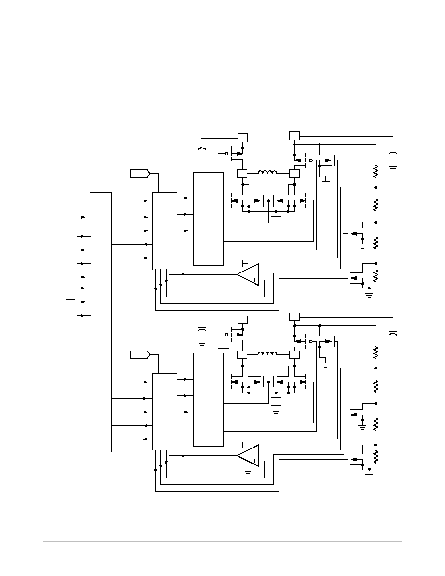
NCN6004A
http://onsemi.com
23
When the output voltage reaches the specified value
(1.80 V or 3.0 V or 5.0 V), Q1 and Q16 are switched
OFF immediately to avoid over voltage on the output
load. In the mean time, the two extra NMOS Q2 and
Q3 are switched ON to fully discharge any current
stored into the inductor, avoiding ringing and
voltage spikes over the system. Figure 16 illustrates
the theoretical basic waveforms present in the
DC/DC converter.
The control block gives the logic states according to the
bits provided by the external
mP. These controls bits are
applied to the selected DC/DC converter to generate the
programmed output voltage. The MOS drive block includes
the biases necessaries to drive the NMOS and PMOS
devices as depicted in the block diagram given Figure 15.
U1
R2
R3
R4
Vref
LOGIC CONTROL
#
A
V0
PWR_ON
Overload
VCC_OK
Voltage Regulation
GND
Vcc
Vref_1.8/3/5 V
PGM
CARD_SEL
A0
A1
A2
DC/DC MUL
TIPLEXED CONTROLS
PWR_ON
A3
Q1
Q4
Q15
Q16
L1
C1
Vcc
PWR_GND
CRD_VCC_A
GND
GND
MIXED LOGIC /
ANALOG BLOCK
G_Q1
G_Q2
G_Q3
G_Q4
G_HIZ
GND
G_Q7
Q3
Q2
Q5
V1
V
out
R1
Q7
Q6
5.0 V
5.0 V
GND
Figure 15. Basic DC/DC Converter Diagram
CS
10
m
F
C2
GND
10
m
F
GND
22
m
H
29
27
26
25
28
U2
R6
R7
R8
Vref
LOGIC CONTROL
#
A
V0
PWR_ON
Overload
VCC_OK
Voltage Regulation
GND
Vcc
Vref_1.8/3/5 V
Q8
Q11
Q17
Q18
L2
C3
Vcc
PWR_GND
CRD_VCC
GND
GND
MIXED LOGIC /
ANALOG BLOCK
G_Q1
G_Q2
G_Q3
G_Q4
G_HIZ
GND
G_Q7
Q10
Q9
Q12
V1
V
out
R5
Q14
Q13
3.0 V
5.0 V
GND
10
m
F
C4
GND
10
m
F
GND
22
m
H
32
34
35
36
33

NCN6004A
http://onsemi.com
24
Since the output inductor L1 and the reservoir capacitor
C1 carry relative high peak current, low ESR devices must
be used to prevent the system from poor output voltage
ripple and low efficiency. Using ceramic capacitors, X5R or
X7R type, are recommended, splitting the 10
mF in two
separate parts when there is a relative long distance between
the CRD_VCC_x output pin and the card VCC input. On the
other hand, the inductor shall have an ESR below 1.0
W to
achieve the high efficiency over the full temperature range.
However, inductor with 2.0
W
ESR can be used when a slight
decrease of the efficiency is acceptable at system level.
Ton Toff
CRD_VCC Charged
Charge CRD_VCC
Next CRD_VCC Charge
Q1 / Q4
Q2 / Q3
IL
(Time is not to scale)
CRD_VCC
CRD_VCC Voltage Regulated
Ipeak
V
ripple
Q5/Q6
Figure 16. Theoretical DC/DC Operating
When the CRD_VCC is programmed to zero volt, or when
the card is extracted from the socket, the active pull down Q5
rapidly discharges the output reservoir capacitor, making
sure the output voltage is below 0.40 V when the card slides
across the contacts.
Based on the experiments carried out during the
NCN6004A characterization, the best comprise, at time of
printing this document, is to use two
4.7
mF/10 V/ceramic/X7R capacitor in parallel to achieve
the CRD_VCC filtering. The ESR will not extend 50 m
W
over the temperature range and the combination of standard
parts provide an acceptable ≠20% to +20% tolerance,
together with a low cost. Table 6 shows a quick comparison
between the most common type of capacitors. Obviously,
the capacitor must be SMD type to achieve the extremely
low ESR and ESL necessary for this application.
Figure 17 illustrates the CRD_VCC ripple observed in the
NCN6004A demo board running with X7R ceramic
capacitors.
Table 6. Ceramic/Electrolytic Capacitors Comparison
Manufacturer
Type/Series
Format
Max Value
Tolerance
Typ. Z @ 500 kHz
MURATA
CERAMIC/GRM225
0805
10
m
F/6.3 V
-20% /+20%
30 m
W
MURATA
CERAMIC/GRM225
0805
4.7
m
F/6.3 V
-20% /+20%
30 m
W
VISHAY
Tantalum/594C/593C
1206
10
m
F/16 V
450 m
W
VISHAY
Electrolytic/94SV
1812
10
m
F/10 V
-20%/+20%
400 m
W
Miscellaneous
Electrolytic Low Cost
1812
10
m
F/10 V
-35%/+50%
2.0
W

NCN6004A
http://onsemi.com
25
Figure 17. Typical CRD_VCC Ripple Voltage
NOTE:
Operating conditions under full output load.
Figure 18. Typical Card Voltage Turn ON and Start-up
Sequence
Figure 19. Typical Card Supply Turn OFF
58
60
62
64
66
68
70
72
74
2.5
3.0
3.5
4.0
4.5
5.0
5.5
Figure 20. CRD_VCC Efficiency as a Function of the
Input Supply Voltage
V
bat
(V)
Ef
f (%)
V
out
= 1.8 V
V
out
= 5.0 V
V
out
= 3.0 V
L
out
= 22
m
H
ESR = 2
W
The curves in Figure 20, illustrate the typical behavior
under full output current load (35 mA, 60 mA and 65 mA),
according to EMV specifications.
During the operation, the inductor is subject to high peak
current as depicted in Figure 21 and the magnetic core must
sustain this level of current without damage. In particular,
the ferrite material shall not be saturated to avoid
uncontrolled current spike during the charge up cycle.
Moreover, since the DC/DC efficiency depends upon the
losses developed into the active and passive components,
selecting a low ESR inductor is preferred to reduce these
losses to a minimum.

NCN6004A
http://onsemi.com
26
Figure 21. Typical Output Voltage Ripple
Test conditions: Input V
CC
voltage = 5.0 V, Current = 200 mA /div,
T
amb
= +20
∞
C
According to the ISO7816-3 and EMV specifications, the
interface shall limits the CRD_VCC output current to
200 mA maximum, under short circuit conditions. The
NCN6004A supports such a parameter, the limit being
depending upon the input and output voltages as depicted
in Figure 22.
Figure 22. Output Current Limit
Figure 23. Output Current Limit as a Function
of the Temperature
180
160
140
120
100
80
60
40
20
0
6
5
4
3
2
V
bat
(V)
I
out
(mA)
V
o
= 5.0 V
V
o
= 3.0 V
V
o
= 1.8 V
100
-5.0
-25
TEMPERATURE (
∞
C)
15
35
55
75
95
115
160
150
140
130
120
110
I
out
(mA)
V
o
= 5.0 V
V
o
= 3.0 V
V
o
= 1.8 V
I
O(max)
= F(V
bat
)
Beside the continuous current capability, the smart card
power supply must be capable of providing a 100 mA pulsed
current during the data transaction. The ISO7816-3,
paragraph
4.3.2, defines this 400 ns pulse as a function of the
environment. As a matter of fact, this pulse does not come
solely from the NCN6004A DC/DC converter, but the
reservoir capacitor and the associated PCB tracks shall be
considered as well.

NCN6004A
http://onsemi.com
27
CLOCK DIVIDER
The main purpose of the built in clock generator is four
folds:
1. Adapts the voltage level shifter to cope with the
different voltages that might exist between the
MPU and the Smart Card
2. Provides a frequency division to adapt the Smart
Card operating frequency from the external clock
source.
3. Control the clock state according to the smart card
specification.
4. Provides an input clock re-routing to route the
CLOCK_IN_A and CLOCK_IN_B signals to
either CRD_CLK_A or CRD_CLK_B output pins.
In addition, the NCN6004A adjusts the signal coming
from the microprocessor to get the Duty Cycle window as
defined by the ISO7816-3 specification.
The logic input pins CARD_SEL, A0, A1, PGM, I/O and
RESET fulfill the programming functions when both PGM
and CS are Low. The clock input stage (CLOCK_IN) can
handle a 40 MHz frequency maximum, the divider being
capable to provide an 1:8 ratio. Of course, the ratio must be
defined by the engineer to cope with the Smart Card
considered in a given application and, in any case, the output
clock (CRD_CLK_A and CRD_CLK_B) shall be limited to
20 MHz maximum when the system is considered to operate
over the full temperature range.
A2
A0
A1
PGM
CS
CLOCK_IN_B
1
2
3
CRD_CLK_A
LEVEL SHIFTER
& CONTROL
CRD_VCC_A
CARD_A & CARD_B CLOCK
CRD_VCC_A
A2
CARD_SEL
CRD_CLK_B
LEVEL SHIFTER
& CONTROL
CRD_VCC_B
CARD_A
CARD_B
DC/DC BLOCK_A
CRD_VCC_B
DC/DC BLOCK_B
CLOCK_IN_A
CLOCK_A
DIVIDER
CLOCK_AB DIVIDER
MUX_A&B
MUX_A&B
LOGIC
CONTROL
Figure 24. Simplified Frequency Divider and Programming Functions
In order to avoid any duty cycle out of the frequency smart
card ISO7816-3 and EMV specifications, the clock divider
is synchronized by the last flip flop, thus yielding a constant
50% duty cycle, regardless of the divider ratio.
Consequently, the output CRD_CLK_A or CRD_CLK_B
frequency division can be delayed by eight CLOCK_IN
pulses and the microcontroller software must take this delay
into account prior to launch a new data transaction.

NCN6004A
http://onsemi.com
28
CRD_CLK
CLOCK_IN
CLOCK : 2
CLOCK : 4
CLOCK : 8
A0
A1
A2
A3
Clock is updated upon CLOCK :8 rising edge
These bits program
Internal CLOCK divider
CLOCK programming is activated
by the PGM rising edge.
CLOCK = 1:1 ratio
CARD_SEL
Figure 25. Clock Programming Timings
CS
PGM
The example given in Figure 25 highlights the delay
coming from the internal clock duty cycle
re-synchronization. Since the clock signal is asynchronous,
it is up to the programmer to make sure the next card
transaction is not activated before, respectively, either the
CRD_CLK_A or CRD_CLK_B signal has been updated.
Generally speaking, such a delay can be derived from the
maximum clock frequency provided to the
interface.
Figure 26. Card Clock 1/2 Divider Operation

NCN6004A
http://onsemi.com
29
Figure 27. Clock Divider: 8 to 1 Operation
Figure 28. Clock Divider Timing Details
Figure 29. Clock Divider: Run to Stop High Operation

NCN6004A
http://onsemi.com
30
The input clock A and B can be re routed to either
CRD_CLK_A or CRD_CLK_B output pins by using the
programming function as defined in Table 2 and Table 7. The
clock signals can have any frequency value necessary to
handle a given type of card (asynchronous or synchronous).
These clock signals can be multiplexed at any time, but the
system must be locked in a safe state prior to make such a
change. In particular, the designer must make sure that A and
B cards can support such a hot change prior to change the
related clocks.
Table 7. Programming Clock Routing
STATE
CS
PGM
A3
A2
A1
A0
CARD_SEL
CRD_CLK_A
CRD_CLK_B
0E
0
0
1
1
1
0
1
CLK_D_A
-
Default
0F
0
0
1
1
1
1
1
CLK_D_B
-
-
0E
0
0
1
1
1
0
0
-
CLK_D_B
Default
0F
0
0
1
1
1
1
0
-
CLK_D_A
-
On the other hand, the slope of the CRD_CLK_x signal
can be set to either FAST or SLOW, depending upon the
frequency of the output clock. This selection is achieved by
programming the chip according to Table 8.
Table 8. Output Clock Slope Selection
STATE
CS
PGM
A3
A2
A1
A0
CARD_SEL
CLOCK SLOPE
$03
0
0
0
0
1
1
1
SLOW
Default
$0B
0
0
1
0
1
1
1
FAST
-
$03
0
0
0
0
1
1
0
SLOW
Default
$0B
0
0
1
0
1
1
0
FAST
-
Figure 30. Typical Rise and Fall Time in Fast and
Slow Operating Mode
PARALLEL OPERATION
When two or more NCN6004A parts operate in parallel on
a common digital bus, the Chip Select pin allows the
selection of one chip from the bank of the paralleled devices.
Of course, the external MPU shall provide one unique CS
line for each of the NCN6004A considered interface. When
a given interface is selected by CS = L, all the logic inputs
becomes active, the chip can be programmed or/and the
external card can be accessed. When CS = H, all the input
logic pins are in the high impedance state, thus leaving the
bus available for other purpose.
The pull up resistors connected on each logic input lines on
the MPU side (see block diagram in Figure 30), can be either
activated (connected to V
CC
) or disconnected, depending
upon the logic state present at EN_RPU, pin 45. When these
resistors are disconnected, it is the system responsibility to
set up the external pull up resistors according to the
application's requirements.
When the device operates in the multiplexed mode
(MUX_MODE = High), the internal card #B pull up
resistors are connected to V
CC
, regardless of the EN_RPU
logic state.
On the other hand, when CS = H, the CRD_IO and
CRD_RST hold the previous I/O and RESET logic state, the
CRD_CLK being either active or stopped and the
CRD_VCC output voltage will maintain is previous value,
according to the programmed state forced by the MPU.

NCN6004A
http://onsemi.com
31
Figure 31. Parallel Operation Wiring
"
MUX_MODE = Low
13
10
11
12
9
19
18
17
16
15
RESET_A
C4_A
C8_A
CLK_IN_A
I/O_A
I/O_B
C8_B
C4_B
RESET_B
CLK_IN_B
44
5
MUX_MODE
CARD_SEL
BUFFERS
BUFFERS
BUFFER
BUFFER
BUFFER
I/O_A
BUFFER
I/O_B
CARD_B
CARD_A
CLK_A
CLK_B
23
22
21
24
37
38
39
40
30
31
CLOCK GEN.
CLOCK GEN.
MULTIPLEX &
CLOCK DIVIDER
CARD
GND
LOGIC
CONTROL
POR
T
A
POR
T
B
CTL
MICRO CONTROLLER
When the chip operates in the parallel mode, all the logic
signals must be independently controlled by the
microcontroller as depicted in Figure 31. The MUX_MODE
pin must be hardwired to VCC and it cannot be changed
during an operation of the chip. Beside this parameter, the
user must select to force or not the internal pull up resistors
as defined by the EN_RPU logic state.
Figure 32. Multiplexed Operation Wiring
"
MUX_MODE = High
13
10
11
12
9
19
18
17
16
15
RESET_A
C4_A
C8_A
CLK_IN_A
I/O_A
I/O_B
C8_B
C4_B
RESET_B
CLK_IN_B
44
5
MUX_MODE
CARD_SEL
BUFFERS
BUFFERS
BUFFER
BUFFER
BUFFER
I/O_A
BUFFER
I/O_B
CARD_B
CARD_A
CLK_A
CLK_B
23
22
21
24
37
38
39
40
30
31
CLOCK GEN.
CLOCK GEN.
POR
T
A
POR
T
B
CTL
MICRO CONTROLLER
MULTIPLEX &
CLOCK DIVIDER
CARD
VCC
LOGIC
CONTROL
In the multiplexed mode, the microprocessor CARD_B
side pins are not connected, the logic signals and the I/O line
being shared with CARD_A associated with the CRD_SEL
control bit: Figure 32. A key point is to make sure there is no
connection associated with the I/O_B pin since this pin is
internally shared with the I/O line transaction. The
CLK_IN_A and CLK_IN_B signals are independent and
can be routed to any of the card thanks to the built-in clock
multiplexer.
DATA I/O LEVEL SHIFTER
The built in structure provides a level shifter on each card
output signals, the I/O line being driven differently as
depicted in Figure 33. Since the NCN6004A can operate in
either a multiplexed or parallel mode, provisions have been
made to route the I/O_A input pin to either CARD_A or
CARD_B.
In both case, the I/O pins are driven by an open drain
structure with a 20 k
W pull up resistor as shown Figure 33.
To achieve the 0.80
ms maximum rise time requested by the
EMV specifications, an accelerator circuit is added on both
side of each I/O line. These pulsed circuits yield boost
current to charge the stray capacitance, thus accelerating the
positive going slope of the I/O signal. On the other hand, the
active pull down NMOS device Q5 provides a low
impedance to ground during the battery up and DC/DC
start-up phase, avoiding any uncontrolled voltage spikes on
the I/O lines.

NCN6004A
http://onsemi.com
32
MUX_MODE = Low
"
PARALLEL OPERATION
The bi-directional switch Q9 is OFF and the I/O signals
are routed straightforward to their appropriate outputs. The
two I/O lines can operate simultaneously, depending upon
the
mP capabilities, regardless of the CARD_SEL signal
logic level.
The pull up resistors, on the
mP side of each I/O line, can
be connected or not as defined by the EN_RPU signal.
MUX_MODE = High
"
MULTIPLEXED OPERATION
The bi-directional switch Q9 is ON and the I/O_A pin is
used to handle data for CARD_A and CARD_B. The signal
is routed to the appropriate card by means of the
CARD_SEL logic signal. In this mode, the I/O_B pin 19
must be left open since the internal data signal will be
present on this pin.
Moreover, since R1 and R3 are in parallel, the pull up
resistor R1 is automatically disconnected to maintain the I/O
line impedance to 20 k
W (typical), what ever be the
EN_RPU logic level. This feature makes sure the current
flowing trough the external card is limited to 500
mA during
a low level state.
24
CRD_I/O_A
BI-DIRECTIONNAL DATA TRANSFERT
42
ANLG_VCC
CRD_VCC_A
9
29
I/O_A
I/O_B
CRD_I/O_B
Q1
Q2
Q3
Q5
GND
CONTROL LOGIC
37
19
BI-DIRECTIONNAL DATA TRANSFERT
Q6
Q11
Q7
Q10
CONTROL LOGIC
CARD_SEL
PWR_ON
5
44
32
CRD_VCC_B
MUX_MODE
45
EN_RPU
Q9
Q10
Q11
R1
R2
R4
Q4
Q8
& Level Shifter
& Level Shifter
CRD_VCC_A
ANLG_VCC
Figure 33. Dual Bi-directional I/O Line Level Shifter and Multiplex
R3
GND
CRD_VCC_B
ANLG_VCC
CS
7
8
6
PGM

NCN6004A
http://onsemi.com
33
NOTE:
Both sides of the interface run with open drain load
(worst case condition)
Figure 34. Typical I/O Rise and Fall Time
ESD Protection
The NCN6004A includes silicon devices to protect the
pins against the ESD spikes voltages. To cope with the
different ESD voltages developed across these pins, the built
in structures have been designed to handle either 2 kV, when
related to the microcontroller side, or 8 kV when connected
with the external contacts. Practically, the CRD_RST,
CRD_CLK, CRD_IO, CRD_C4 and CRD_C8 (both A and
B sections) pins can sustain 8 kV, the maximum short circuit
current being limited to 15 mA. The CRD_VCC_A and
CRD_VCC_B pins have the same ESD protection, but can
source up to 65 mA continuously each, the absolute
maximum current being 150 mA per section.
Security Features
In order to protect both the interface and the external smart
card, the NCN6004A provides security features to prevent
catastrophic failures as depicted here after.
Pin Current Limitation: in case of a short circuit to
ground, the current forced by the device is limited to 10 mA
for any pins, except CRD_CLK_A and CRD_CLK_B pins
which are both limited to 70 mA. No feedback is provided
to the external MPU.
DC/DC Operation: The internal circuit continuously
senses the CRD_VCC_A and CRD_VCC_B voltages and,
in the case of either over or under voltage situation, update
the STATUS register accordingly. This register can be read
out by the MPU but no interrupts are activated.
DC/DC Overload: When an overload is sensed across the
CRD_VCC_A or CRD_VCC_B output, during either the
power on sequence or when the system was previously
running, the NCN6004A generates an interrupt by pulling
down the INT pin. It is up to the microcontroller to identify
the origin of the overload by reading the STATUS pin
accordingly.
Battery Voltage: Both the Positive going and the
Negative going voltage are detected by the NCN6004A, a
POWER_DOWN sequence and the STATUS register being
updated accordingly. The external MPU can read the
STATUS pin to take whatever is appropriate to cope with the
situation. The NCN6004A does not provide any further
internal voltage regulation.

NCN6004A
http://onsemi.com
34
TEST BOARD SCHEMATIC DIAGRAM
1
TP1
Det_B
R2
4.7 k
R1
4.7 k
1
2
4
3
S1
SWITCH
1
2
J3
CLK_A
1
2
J8
CLK_B
1
TP6
RST_B
1
TP2
CLK_B
1
TP3
C4_B
1
TP4
C8_B
1
TP5
IO_B
1
TP12
Det_A
1
TP7
RST_A
1
TP8
CLK_A
1
TP10
C8_A
1
TP9
C4_A
1
TP11
IO_A
C12
CS
7
PWR_ON
8
ST
A
TUS
46
A0
1
A1
2
CARD_SEL
5
PGM
6
I/O_A
9
RESET_A
10
C4_A
11
C8_A
12
CLK_IN_A
13
PWR_VCC_A
28
PWR_GND
36
CRD_DET_A
20
CRD_VCC_A
29
CRD_CLK_A
30
CRD_IO_A
24
CRD_DET_B
41
CRD_VCC_B
32
CRD_CLK_B
31
CRD_IO_B
37
CRD_RST_A
23
CRD_RST_B
38
L2a
27
L1a
26
L1b
34
L2b
35
A2
3
A3
4
EN_RPU
45
CRD_C4_A
22
CRD_C8_A
21
CRD_C4_B
39
CRD_C8_B
40
PWR_VCC_B
33
PWR_GND
25
MUX_MODE
44
INT
47
ANLG_GND
14
ANLG_GND
48
ANLG_VCC
42
ANLG_GND
43
CLK_IN_B
15
C8_B
16
C4_B
17
RESET_B
18
I/O_B
19
U1
NCN6004
I/O 7
Swa 10
Swb
9
C4 4
CLK 3
RST 2
Vcc 1
GND 5
VPP
6
C8
8
ISO7816
J2
SMARTCARD_B
I/O
7
Swa
10
Swb
9
C4
4 CLK
3 RST
2
Vcc
1
GND
5
VPP
6
C8
8
ISO7816
J12
SMARTCARD_A
+
C11
100 nF, X7R
+
C7
4.7uF, X7R
+
C5
+ C6
+
C8
R15
10 k
R12
1.5 k
R11
1.5 k
R14
10 k
R13
1.5 k
R10
1.5 k
R16
0R
C10
C_CLK_B
C9
R17
0R
C13
220 nF
C14
220 nF
1
TP20
A0
1
TP21
A1
1
TP19
A2
TP18
A3
1
TP17
Card_Sel
1
TP16
PGM
1
TP15
CS
1
TP23
Status
1
TP24
INT
1
TP22
PWR_ON
1
2
3
4
5
6
7
8
9
10
11
12
13
14
15
16
17
18
19
20
21
22
23
24
25
26
27
28
29
30
31
32
33
34
35
36
37
38
39
40
41
42
43
44
45
46
47
48
49
50
J1
CONTROL & I/O
R4
1.5k
R5
1.5k
VCC
VCC
GND
GND
GND
VCC
GND
GND
GND
VCC
VCC
VCC
VCC
1
2
3
4
5
6
7
8
9
R3
8x10k
GND
1
2
J5
MPU_CLK
1
2
J7
EXT_CLK
GND
1
2
J4
MPU_CLK
1
2
J6
EXT_CLK
GND
GND
GND
VCC
D1
LED
D2
LED
L1
L2
22
m
H
GND
D5
CARD_A_INS
1
2
J10
CRD_VCC_A
Q2
2N2222
GND
D6
CRD_VCC_A
1
2
J9
CRD_VCC_B
GND
GND
D3
CRD_B_INS
GND
GND
Q1
2N2222
D4
CRD_VCC_B
A0
A1
A2
A3
CARD_SEL
PGM
CS
PWR_ON
MUX_MODE
EN_RPU
ST
A
TUS
INT
I/O_A
RESET_A
C4_A
C8_A
CLK_IN_A
CLK_IN_B
C8_B
C4_B
RESET_B
I/O_B
E
IO_A
VCC_A
RST_A
CLK_A
1
2
J13
GROUND
1
2
J14
GROUND
1
2
J11 GROUND
C1
100 nF
C2
100 nF
GND
VCC
VCC_B
C3
10
m
F
1
TP13
I/O_A
1
TP14
I/O_B
ST
A
TUS
CLK_IN
IO_B
GND
Figure 35. Test Board Schematic Diagram
22
m
H
4.7
m
F, X7R
4.7
m
F, X7R
4.7
m
F, X7R
10
m
F, X7R
GND

NCN6004A
http://onsemi.com
35
Figure 36. Demo Board PCB Top Overlay
NCN6004A
http://onsemi.com
36
Figure 37. Demo Board PCB Top Layer

NCN6004A
http://onsemi.com
37
Figure 38. Demo Board PCB Bottom Layer
NOTE:
Note: the demo board is built with a four layers PCB, the internal ones being dedicated to V
CC
and GND
planes.

NCN6004A
http://onsemi.com
38
PIN FUNCTIONS AND DESCRIPTION
4
. . . . . . .
POWER SUPPLY SECTION
10
. . . . . . . . . . . . . . . .
DIGITAL INPUT SECTION @ 2.70 < V
CC
< 5.50V,
Normal Operating Mode
11
. . . . . . . . . . . . . . . . . . .
CARD INTERFACE SECTION @ 2.70 < V
CC
< 5.50V,
Normal Operating Mode
12
. . . . . . . . . . . . . . . . . . .
DIGITAL DYNAMIC SECTION NORMAL OPERATING
MODE
13
. . . . . . . . . . . . . . . . . . . . . . . . . . . . . . . . . . .
DIGITAL DYNAMIC SECTION PROGRAMMING MODE
13
. . . . . . . . . . . . . . . . . . . . . . . . . . . . . . . . . . . . . . . . . .
PROGRAMMING AND STATUS FUNCTIONS
14
. . . . . . . . . . . . . . . . . . . . . . . . . . . . . . . . . . . . . . . . . .
SYSTEM STATES UPON START UP
16
. . . . . . . .
PARALLEL/MULTIPLEXED OPERATION MODES
17
. . . . . . . . . . . . . . . . . . . . . . . . . . . . . . . . . . . . . . . . . .
CARD POWER SUPPLY TIMING
18
. . . . . . . . . . .
POWER DOWN OPERATION
18
. . . . . . . . . . . . . .
CARD DETECTION
20
. . . . . . . . . . . . . . . . . . . . . . .
POWER MANAGEMENT
21
. . . . . . . . . . . . . . . . . .
OUTPUT VOLTAGE PROGRAMMING
21
. . . . . . .
DC/DC CONVERTER
22
. . . . . . . . . . . . . . . . . . . . . .
CLOCK DIVIDER
27
. . . . . . . . . . . . . . . . . . . . . . . . .
PARALLEL OPERATION
30
. . . . . . . . . . . . . . . . . .
DATA I/O LEVEL SHIFTER
31
. . . . . . . . . . . . . . . . .
ESD PROTECTION
33
. . . . . . . . . . . . . . . . . . . . . . .
SECURITY FEATURES
33
. . . . . . . . . . . . . . . . . . . .
TEST BOARD SCHEMATIC DIAGRAM
34
. . . . . .
Figures
Figure 1: Pin Diagram
2
. . . . . . . . . . . . . . . . . . . .
Figure 2: Typical Applications
2
. . . . . . . . . . . . .
Figure 3: Block Diagram
3
. . . . . . . . . . . . . . . . . .
Figure 4: Programming Sequence
14
. . . . . . . . .
Figure 5: Reading ANLG_VCC Status
16
. . . . . .
Figure 6: Simplified MUX_MODE Logic and
Multiplex CIrcuit
17
. . . . . . . . . . . . . . . . . . . . . . . . . .
Figure 7: Card Power Supply Turn ON and
Shut OFF Typical Sequence
18
. . . . . . . . . . . . . . .
Figure 8: Card Power Down Sequence
18
. . . . .
Figure 9: Power Down Sequence
19
. . . . . . . . . .
Figure 10: Power Down Sequence: Timing Details
19
. . . . . . . . . . . . . . . . . . . . . . . . . . . . . . . . . . . . . . . . . .
Figure 11: Typical Interrupt Sequence
20
. . . . . .
Figure 12: Card Power Supply Controls
21
. . . . . . . . . . . . . . . . . . . . . . . . . . . . . . . . . . . . . . . . . .
Figure 13: Power On Sequence Timing
22
. . . . .
Figure 14: Power On and CARD_SEL Sequence
Timings
22
. . . . . . . . . . . . . . . . . . . . . . . . . . . . . . . . .
Figure 15: Basic DC/DC Converter Diagram
23
. . . . . . . . . . . . . . . . . . . . . . . . . . . . . . . . . . . . . . . . . .
Figure 16: Theoretical DC/DC Operating
24
. . . . . . . . . . . . . . . . . . . . . . . . . . . . . . . . . . . . . . . . . .
Figure 17: Typical CRD_VCC Ripple Voltage
25
. . . . . . . . . . . . . . . . . . . . . . . . . . . . . . . . . . . . . . . . . .
Figure 18: Typical Card Voltage Turn ON and Start-up
25
. . . . . . . . . . . . . . . . . . . . . . . . . . . . . . . . . . . . . . . . . .
Figure 19: Typical Card Supply Turn OFF
25
. . . . . . . . . . . . . . . . . . . . . . . . . . . . . . . . . . . . . . . . . .
Figure 20: CRD_VCC Efficiency as a Function of the
Input Supply Voltage
25
. . . . . . . . . . . . . . . . . . . . .
Figure 21: Typical Output Voltage Ripple
26
. . . . . . . . . . . . . . . . . . . . . . . . . . . . . . . . . . . . . . . . . .
Figure 22: Output Current Limit
26
. . . . . . . . . . .
Figure 23: Output Current Limit as a Function of the
Temperature
26
. . . . . . . . . . . . . . . . . . . . . . . . . . . . .
Figure 24: Simplified Frequency Divider and
Programming Functions
27
. . . . . . . . . . . . . . . . . .
Figure 25: Clock Programming Timings
28
. . . .
Figure 26: Card Clock
Ω
Divider Operation
28
. . . . . . . . . . . . . . . . . . . . . . . . . . . . . . . . . . . . . . . . . .
Figure 27: Clock Divider: 8 to 1 Operation
29
. . . . . . . . . . . . . . . . . . . . . . . . . . . . . . . . . . . . . . . . . .
Figure 28: Clock Divider Timing Details
29
. . . . . . . . . . . . . . . . . . . . . . . . . . . . . . . . . . . . . . . . . .
Figure 29: Clock Divider: Run to Stop High Operation
29
. . . . . . . . . . . . . . . . . . . . . . . . . . . . . . . . . . . . . . . . . .
Figure 29: Typical Rise and Fall Time in Fast and Slow
Operating Mode
30
. . . . . . . . . . . . . . . . . . . . . . . . . .
Figure 30: Parallel Operation Wiring
"
MUX_MODE = High
30
. . . . . . . . . . . . . . . . . . . . . . .
Figure 31: Multiplexed Operation Wiring
"
MUX_MODE = Low
31
. . . . . . . . . . . . . . . . . . . . . . .
Figure 32: Dual Bi-directional I/O line Level Shifter
and Multiplex
31
. . . . . . . . . . . . . . . . . . . . . . . . . . . .
Figure 33: Typical I/O Rise and Fall Time
32
. . . . . . . . . . . . . . . . . . . . . . . . . . . . . . . . . . . . . . . . . .
Figure 34: Test Board Schematic Diagram
33
. . . . . . . . . . . . . . . . . . . . . . . . . . . . . . . . . . . . . . . . . .
Figure 35: Demo Board PCB Top Overlay
34
. . . . . . . . . . . . . . . . . . . . . . . . . . . . . . . . . . . . . . . . . .
Figure 37: Demo Board PCB Top Layer
36
. . . . . . . . . . . . . . . . . . . . . . . . . . . . . . . . . . . . . . . . . .
Figure 38: Demo Board PCB Bottom Layer
37
. . . . . . . . . . . . . . . . . . . . . . . . . . . . . . . . . . . . . . . . . .
Table 1 :Programming and Reading Basic Functions
14
. . . . . . . . . . . . . . . . . . . . . . . . . . . . . . . . . . . . . . . . . .
Table 2: Programming Functions
15
. . . . . . . . . .
Table 3: Status Pins Data
16
. . . . . . . . . . . . . . . . .
Table 4: Operating Conditions Upon Start-up
16
. . . . . . . . . . . . . . . . . . . . . . . . . . . . . . . . . . . . . . . . . .
Table 5: Card Detection Polarity
20
. . . . . . . . . . .
Table 6: Ceramic/Electrolytic Capacitors Comparison
24
. . . . . . . . . . . . . . . . . . . . . . . . . . . . . . . . . . . . . . . . . .
Table 7: Programming Clock Routing
30
. . . . . .
Table 8: Output Clock Slope Selection
30
. . . . .

NCN6004A
http://onsemi.com
39
ABBREVIATIONS
L1a and L1b
DC/DC external inductor #A
CRD_VCC_A
Interface IC Card #A Power
Supply Line
L2a and L2b
DC/DC external inductor #B
CRD_CLK_A
Interface IC Card #A Clock In-
put
Cout
Output Capacitor
CRD_RST_A
Interface IC Card #A RESET
Input
CRD_VCC
Card Power Supply Input
CRD_IO_A
Interface IC Card #A Data link
VCC
MPU Power Supply Voltage
CRD_C4_A
Interface IC Card #A Data
Control
Icc
Current at card VCC pin
CRD_C8_A
Interface IC Card #A Data
Control
Class A
5 V Smart Card
CRD_DET_A
Card insertion/extraction
detection
CS
Chip Select
CARD_SEL
Card #A/B Selection bit
CRD_CLK_B
Interface IC Card #B Clock In-
put
CRD_IO_B
Interface IC Card #B Data link
EN_RPU
Enable/Disable internal pull up
CRD_IO_B
Interface IC Card #B RESET
Input
PGM
Chip Programming Mode
EMV
Euro Card Master Card Visa
ISO
International Standards Orga-
nization
Class B
3 V Smart Card
CRD_VCC_B
Interface IC Card #B Power
Supply Line
ANLG_VCC = VCC = V
bat
Input Voltage
CRD_C4_B
Interface IC Card #B Data
Control
PWR_ON
Chip Power On bit
CRD_C8_A
Interface IC Card #B Data
Control
MUX_MODE
Card Multiplex or Parallel Op.
CRD_DET_B
Card insertion/extraction
detection
T0
Smart Card Data transfer pro-
cedure by bytes
T1
Smart Card Data transfer pro-
cedure by strings
m
C
Microcontroller

NCN6004A
http://onsemi.com
40
48 LEADS, TQFP EP
CASE 932F-01
ISSUE A
…………
…………
…………
«««
«««
«««
A1
A
T-U
M
0.200
Z
AB
4 PL
48
37
36
1
25
12
13
24
T
B1
B
U
V
V1
NOTES:
1. DIMENSIONS AND TOLERANCING PER ASME Y14.5M,
1994.
2. CONTROLLING DIMENSION: MILLIMETER.
3. DATUM PLANE AB IS LOCATED AT BOTTOM OF LEAD
AND IS COINCIDENT WITH THE LEAD WHERE THE LEAD
EXITS THE PLASTIC BODY AT THE BOTTOM OF THE
PARTING LINE.
4. DATUMS T, U, AND Z TO BE DETERMINED AT DATUM
PLANE AB.
5. DIMENSIONS S AND AB TO BE DETERMINED AT
SEATING PLANE AC.
6. DIMENSIONS A AND B DO NOT INCLUDE MOLD
PROTRUSION. ALLOWABLE PROTRUSION IS 0.250 PER
SIDE. DIMENSIONS A AND B DO INCLUDE MOLD
MISMATCH AND ARE DETERMINED AT DATUM PLANE
AB.
7. DIMENSION D DOES NOT INCLUDE DAMBAR
PROTRUSION. DAMBAR PROTRUSION SHALL NOT
CAUSE THE D DIMENSION TO EXCEED 0.350.
8. MINIMUM SOLDER PLATE THICKNESS SHALL BE 0.0076.
9. EXACT SHAPE OF EACH CORNER IS OPTIONAL.
DIM
MIN
MAX
MILLIMETERS
A
7.000 BSC
A1
3.500 BSC
B
7.000 BSC
B1
3.500 BSC
C
0.900
1.100
D
0.170
0.270
E
0.950
1.250
F
0.170
0.230
G
0.500 BSC
H
0.050
0.150
J
0.090
0.200
K
0.500
0.700
L
0
7
M
12 REF
N
0.090
0.160
P
0.250 BSC
R
0.150
0.250
S
9.000 BSC
S1
4.500 BSC
V
9.000 BSC
V1
4.500 BSC
W
0.200 REF
AA
1.000 REF
_
_
_
S
S1
Z
T-U
M
0.200
Z
AC
4 PL
DETAIL Y
AB
AC
G
AD
AC
0.080
W
C E
H
AA
K
L
R
M
TOP & BOT
0.250
GAUGE PLANE
P
AE
AE
T, U, Z
DETAIL Y
N
F
D
J
SECTION AE-AE
T-U
M
0.080
AC
Z
T
EXPOSED PAD
T
5.000 BSC
DETAIL AD
NOTE 9
SEATING PLANE
ON Semiconductor and are registered trademarks of Semiconductor Components Industries, LLC (SCILLC). SCILLC reserves the right to make
changes without further notice to any products herein. SCILLC makes no warranty, representation or guarantee regarding the suitability of its products for any
particular purpose, nor does SCILLC assume any liability arising out of the application or use of any product or circuit, and specifically disclaims any and all
liability, including without limitation special, consequential or incidental damages. "Typical" parameters which may be provided in SCILLC data sheets and/or
specifications can and do vary in different applications and actual performance may vary over time. All operating parameters, including "Typicals" must be
validated for each customer application by customer's technical experts. SCILLC does not convey any license under its patent rights nor the rights of others.
SCILLC products are not designed, intended, or authorized for use as components in systems intended for surgical implant into the body, or other applications
intended to support or sustain life, or for any other application in which the failure of the SCILLC product could create a situation where personal injury or death
may occur. Should Buyer purchase or use SCILLC products for any such unintended or unauthorized application, Buyer shall indemnify and hold SCILLC
and its officers, employees, subsidiaries, affiliates, and distributors harmless against all claims, costs, damages, and expenses, and reasonable attorney fees
arising out of, directly or indirectly, any claim of personal injury or death associated with such unintended or unauthorized use, even if such claim alleges that
SCILLC was negligent regarding the design or manufacture of the part. SCILLC is an Equal Opportunity/Affirmative Action Employer.
PUBLICATION ORDERING INFORMATION
JAPAN: ON Semiconductor, Japan Customer Focus Center
2-9-1 Kamimeguro, Meguro-ku, Tokyo, Japan 153-0051
Phone: 81-3-5773-3850
ON Semiconductor Website: http://onsemi.com
For additional information, please contact your local
Sales Representative.
NCN6004A/D
Literature Fulfillment:
Literature Distribution Center for ON Semiconductor
P.O. Box 5163, Denver, Colorado 80217 USA
Phone: 303-675-2175 or 800-344-3860 Toll Free USA/Canada
Fax: 303-675-2176 or 800-344-3867 Toll Free USA/Canada
Email: ONlit@hibbertco.com
N. American Technical Support: 800-282-9855 Toll Free USA/Canada