 | –≠–ª–µ–∫—Ç—Ä–æ–Ω–Ω—ã–π –∫–æ–º–ø–æ–Ω–µ–Ω—Ç: NCP1000T | –°–∫–∞—á–∞—Ç—å:  PDF PDF  ZIP ZIP |
©
Semiconductor Components Industries, LLC, 2003
March, 2003 - Rev. 6
1
Publication Order Number:
NCP1000/D
NCP1000, NCP1001,
NCP1002
Integrated Off-Line
Switching Regulator
The NCP1000 through NCP1002 series of integrated switching
regulators, combine a fixed frequency PWM controller with an
integrated high voltage power switch circuit. This chip allows for
simple design and minimal parts count for very low cost applications
which utilize an ac input. This chip is designed to power a single ended
topology, typically a discontinuous mode flyback, with secondary side
sensing.
The internal high voltage switch circuit and start-up circuit can
function in continuous operation over a wide range of inputs, from 85
Vac to 265 Vac, and thus can be used in any existing power system in
the world. Though inexpensive, these devices include a number of
features such as undervoltage lockout, over-temperature protection,
bandgap reference and leading edge blanking that make them an
excellent value.
Features
∑
Highly Integrated Solution
∑
Operates Over Universal Input Voltage Range (85 Vac to 265 Vac)
∑
On-board 700 Volt Power Switch Circuit
∑
Minimal External Parts Required
∑
Input Undervoltage Lockout with Hysteresis
∑
Very Low Standby Current
∑
No Minimum Load Requirement
∑
Opto Fail-safe Shutdown Circuit
Typical Applications
∑
Cell Phone Chargers
∑
Wall Adapters
∑
On-board AC-DC Converters
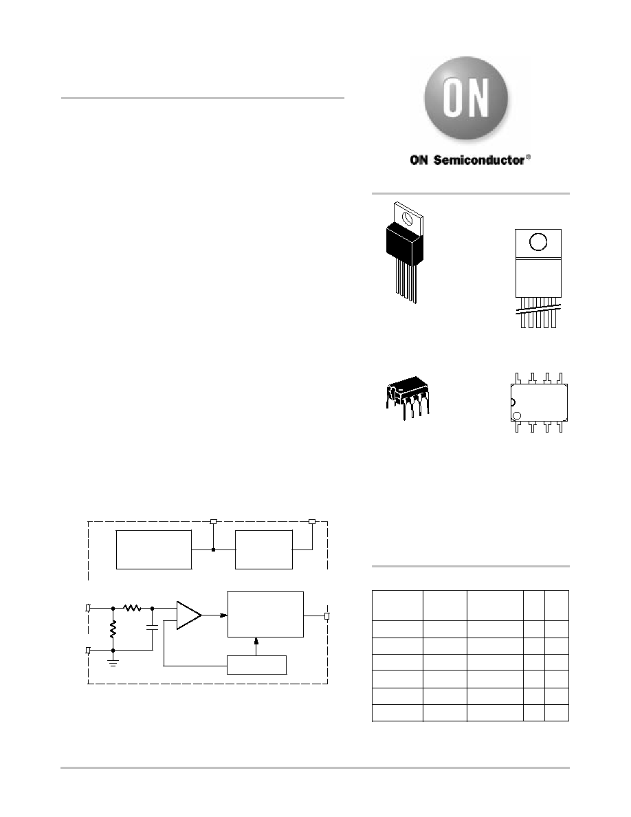
POWER
SWITCH
CIRCUIT
INTERNAL BIAS
UVLO &
OPTO FAIL-SAFE
START-UP
CIRCUIT
V
CC
START-UP
-
+
PWM
COMPARATOR
PWM CONTROL
& POWER
SWITCH CIRCUIT
OSCILLATOR
FEEDBACK
INPUT
GND
Figure 1. Simplified Block Diagram
Device
Package
Shipping
ORDERING INFORMATION*
NCP1000P
DIP-8
50 Units/Rail
NCP1002P
DIP-8
NCP1000T
TO-220
DIP-8
P SUFFIX
CASE 626
1
8
NCP1001T
TO-220
NCP1001P
DIP-8
NCP1002T
TO-220
MARKING
DIAGRAMS
x
= Device Number 0, 1, or 2
A
= Assembly Location
WL
= Wafer Lot
YY, Y = Year
WW
= Work Week
1
8
12
3
45
TO-220
T SUFFIX
CASE 314P
Pin:
1. V
CC
2. Feedback Input
3. Ground
4. Startup
5. Power Switch Circuit
Pin:
1.
V
CC
2.
Feedback Input
3, 6-8
Ground
4.
Startup
5.
Power Switch Circuit
1
5
Ipk
Typ
(A)
Ron
Max
(
W
)
0.5
18
1.0
9
1.5
6
0.5
18
1.0
9
1.5
6
NCP100xP
AWL
YYWW
50 Units/Rail
50 Units/Rail
50 Units/Rail
50 Units/Rail
50 Units/Rail
*Consult factory for additional optocoupler fail-safe
latching, frequency, and current limit options.
NCP100xT
AWLYWW
http://onsemi.com

NCP1000, NCP1001, NCP1002
http://onsemi.com
2
Functional Pin Description
Pin
(DIP-8)
Pin
(TO-220)
Function
Description
1
1
V
CC
Positive input supply voltage. This pin is connected to an external capacitor for
energy storage. The start-up circuit sources current out of this pin to initially
charge the capacitor. When the voltage reaches the upper threshold limit of the
undervoltage lockout circuit, the start-up circuit will turn off, and the power
supply will begin operation. Power is then supplied to the chip via this pin, by
virtue of the auxiliary winding.
2
2
Feedback Input
The error signal from the optocoupler is fed into this input. It is loaded with
a 2.7 k
W
resistor which converts the opto current into a voltage. There
is a 7.0 kHz, single pole, low pass filter between this pin and the error amp
input. A 10 volt clamp is also connected to this pin to protect the device from
ESD damage or overvoltage conditions.
3, 6, 7, 8
3
Ground
Ground reference pin for the circuit. This pin is part of the integrated circuit
leadframe and is electrically common with the tab on the TO-220, and is an
integral part of the heat flow path on the DIP-8 package.
4
4
Start-up
This pin is connected to the bulk DC input voltage supply. It feeds an internal
current source that initially charges up the V
CC
capacitor on power up.
5
5
Power Switch Circuit
The internal power switch circuit is connected between this pin and ground.
This pin connects directly to one end of the transformer primary winding.
MAXIMUM RATINGS
(Notes 1 and 2)
Rating
Symbol
Value
Unit
Power Switch Circuit (Pin 5)
Drain Voltage Range
Drain Current Peak During Transformer Saturation
V
DS
I
DS(pk)
*
0.3 to 700
2.0 I
lim
Max
V
A
Power Supply Voltage Range (Pin 1)
V
clp
*
0.3 to 10
V
Feedback Input (Pin 2)
Voltage Range
Current
V
I(fb)
l
fb
*
0.3 to 10
100
V
mA
Thermal Resistance
P Suffix, Plastic Package Case 626
Junction to Lead
Junction to Air, 2.0 Oz. Printed Circuit Copper Clad
0.36 Sq. Inch
1.0 Sq. Inch
T Suffix, Plastic Package Case 314D
Junction to Case
Junction to Air
R
q
JL
R
q
JA
R
q
JC
R
q
JA
5.0
45
35
2.0
65
∞
C/W
Operating Junction Temperature
T
J
*
40 to 125
∞
C
Storage Temperature
T
stg
*
65 to +150
∞
C
1. This device series contains ESD protection and exceeds the following tests:
Pins 1-3:
Human Body Model 2000 V per MIL-STD-883, Method 3015.
Machine Model Method 200 V.
Pins 4 and 5 are the HV start-up and the drain of the LDMOS device, rated only to the max rating of the part , or 700 V.
2. This device contains Latch-up protection and exceeds
$
200 mA per JEDEC Standard JESD78.

NCP1000, NCP1001, NCP1002
http://onsemi.com
3
ELECTRICAL CHARACTERISTICS
(V
CC
= 8.6 volts, pin 2 grounded, T
J
= 25
∞
C for typical values. For min/max values, T
J
is the
operating junction temperature that applies.)
Characteristics
Symbol
Min
Typ
Max
Unit
OSCILLATOR
Frequency (l
fb
= 1.1 mA) (Note 4) (Figure 7)
T
J
= 25
∞
C
T
J
= 0
∞
C to 125
∞
C
T
J
= -40
∞
C to 125
∞
C
f
OSC
90
85
75
100
-
-
110
115
115
kHz
PWM COMPARATOR
Feedback Input PWM Gain (T
J
= 25
∞
C) (l
fb
= 1.20 mA to 1.30 mA) (Figure 2)
Gain Temperature Coefficient (T
J
= -40
∞
C to T
J
= 125
∞
C) (Note 4)
A
v
D
A
v
-1 10
-
*
136
0.2
-170
-
%/mA
(%/mA)/
∞
C
PWM Duty Cycle (Pin 2)
Maximum (l
fb
= 0.8 mA)
Zero Duty Cycle Current
D
(max)
I
fb
68
1.8
72
-
74
-
%
mA
PWM Ramp
Peak
Valley
V
rpk
V
rvly
-
-
4.1
2.7
-
-
V
START-UP CONTROL AND V
CC
LIMITER
Undervoltage Lockout (Figure 8)
V
CC
Clamp Voltage (I
CC
= 4.0 mA)
Start-Up Threshold (V
clp
Increasing)
Minimum Operating Voltage After Turn-On
Hysteresis
V
clp
V
clp(on)
V
clp(min)
V
H
8.3
8.2
7.2
-
8.55
8.5
7.5
1.0
8.9
8.8
8.0
-
V
Start-Up Circuit, Pin 1 Output Current (Pin 4 = 50 V)
V
CC
= 0 V
V
CC
= 8.0 V
I
start
2.0
1.5
3.4
2.6
4.2
4.2
mA
Minimum Start-Up Voltage (V
CC
= V
clp(on)
-0.2 V, I
start
= 0.5 mA)
V
start
-
14.7
20
V
Auto Restart (C
Pin 1
= 47
m
F, Pin 4 = 50 V) (Note 5)
Duty Cycle
Frequency
D
rst
f
rst
4.0
-
5.0
1.2
6.0
-
%
Hz
Start-Up Circuit Breakdown Voltage (I = 25
m
A) (Note 5)
V
BR(st)
700
-
-
V
Start-Up Circuit Leakage Current (Pin 4 = 700 V
DC
)
T
J
= 25
∞
C
T
J
= -40
∞
C to 125
∞
C
I
leak
-
-
20
30
40
75
m
A
3. Maximum package power dissipation limits must be observed.
4. Tested junction temperature range for this device series: T
low =
-40
∞
C, T
high
= +125
∞
C
5. Guaranteed by design only.

NCP1000, NCP1001, NCP1002
http://onsemi.com
4
ELECTRICAL CHARACTERISTICS
Characteristics
Symbol
Min
Typ
Max
Unit
POWER SWITCH CIRCUIT
Power Switch Circuit On-State Resistance
NCP1000 (I
D
= 50 mA)
T
J
= 25
∞
C
T
J
= 125
∞
C (Note 8)
NCP1001 (I
D
= 100 mA)
T
J
= 25
∞
C
T
J
= 125
∞
C (Note 8)
NCP1002 (I
D
= 150 mA)
T
J
= 25
∞
C
T
J
= 125
∞
C (Note 8)
R
(on)
-
-
-
-
-
-
13
24
7.0
14
4.0
8.0
18
36
9.0
18
6.0
12
W
Power Switch Circuit Breakdown Voltage
(I
D(off)
= 100
m
A, T
J
= 25
∞
C)
V
(BR)
700
-
-
V
Power Switch Circuit Off-State Leakage Current (V
DS
= 650 V)
T
J
= 25
∞
C
T
J
= -40
∞
C to 125
∞
C
I
(off)
-
-
0.25
-
1.0
50
m
A
Switching Characteristics (V
DS
= 50 V, R
L
set for I
D
= 0.7 I
Iim
)
Turn-on Time (90% to 10%)
Turn-of f Time (10% to 90%)
t
on
t
off
-
-
50
50
-
-
ns
CURRENT LIMIT AND THERMAL PROTECTION
Current Limit Threshold (T
J
= 25
∞
C) (Note 9)
NCP1000
NCP1001
NCP1002
I
lim
0.42
0.84
1.26
0.48
0.96
1.43
0.54
1.08
1.6
A
Current Limit, Peak Switch Current
NCP1000 (di/dt = 100 mA/
m
s)
NCP1001 (di/dt = 200 mA/
m
s)
NCP1002 (di/dt = 300 mA/
m
s)
I
pk
-
-
-
0.500
1.000
1.500
-
-
-
A
Opto Fail-safe Protection (Figure 12)
T
J
= 25
∞
C
T
J
= 0
∞
C to 125
∞
C
I
Ofail
-
10
18
-
25
35
mA
Propagation Delay, Current Limit Threshold to Power Switch Circuit Output
(Leading Edge Blanking plus Current Limit Delay)
t
PLH
-
220
-
ns
Thermal Protection (Note 6, 8)
Shutdown (Junction Temperature Increasing)
Hysteresis (Junction Temperature Decreasing)
t
sd
t
H
125
-
140
30
-
-
∞
C
TOTAL DEVICE (Pin 1)
Power Supply Current After UVLO Turn-On
Power Switch Circuit Enabled
NCP1000
NCP1001
NCP1002
Power Switch Circuit Disabled
I
CC1
I
CC2
-
-
-
0.6
1.2
1.4
1.6
1.0
1.6
1.8
2.0
1.25
mA
6. Maximum package power dissipation limits must be observed.
7. Tested junction temperature range for this device series:
T
low
= -40
∞
C
T
high
= +125
∞
C
8. Guaranteed by design only.
9. Actual peak switch current is increased due to the propagation delay time and the di/dt (see Figure 16).

NCP1000, NCP1001, NCP1002
http://onsemi.com
5
0.800
0.700
0.600
0.500
0.400
0.300
0.200
0.100
0.000
DC (%)
0.8
1.4
1.2
1
1.6
1.8
100
10
1.0
90.0
92.0
88.0
86.0
94.0
96.0
98.0
102.0
104.0
1
1.5
0.5
0
2
2.00
V
CC
(V)
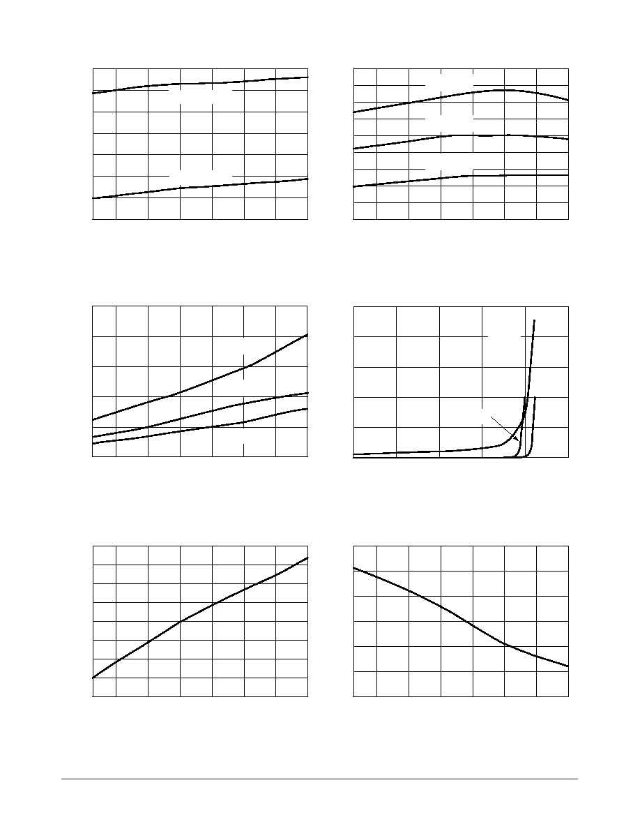
Figure 2. Duty Cycle vs. FB Input Current
Figure 3. I
CC
vs. V
CC
I
CC
(mA)
1
1000
100
100
10
1
10
Figure 4. Charge Time vs. V
CC
Capacitance
Capacitance (
m
F)
Figure 5. Startup Current vs. Startup Voltage
Start-up Voltage (V) (Pin 4)
Start-up Current (mA)
V
CC
Charge T
ime (ms)
Figure 6. Power Switch Circuit
Capacitance vs. Voltage
Switch Voltage (V)
Figure 7. Oscillator Frequency
vs. Temperature
Temperature (
∞
C)
Capacitance (pF)
f
OS
C
, (kHz)
100
10
1000
0
4
5
3
2
6
1
9
1
10
100
1000
1.00
2.50
0.50
1.50
0.00
3.50
4.00
-40
75
50
0
100
-25
125
l
fb
(mA)
7
8
3.00
25
100.0
V
CC
= 4.0 V
NCP1002
NCP1001
NCP1000
NCP1000, NCP1001, NCP1002
http://onsemi.com
6
-40
75
50
0
100
-25
125
25
-40
75
50
0
100
-25
125
25
-40
75
50
0
100
-25
125
25
-40
75
50
0
100
-25
125
25
-40
75
50
0
100
-25
125
25
24.0
22.0
18.0
20.0
16.0
14.0
8.0
1.50
1.45
1.55
1.60
1.65
1.70
1.75
1.40
1.00
1.60
0.80
1.20
0.00
1.80
100
8.40
8.00
V
CC
/UVLO Threshold (V)
7.80
Temperature (
∞
C)
Figure 8. V
CC
/UVLO Threshold vs.
Temperature
Figure 9. Peak Current Limit Threshold
vs. Temperature
Peak Current Limit Threshold (A)
25.0
20.0
15.0
10.0
5.0
0.0
Figure 10. Power Switch Circuit On Resistance
vs. Temperature
Temperature (
∞
C)
Figure 11. Power Switch Circuit Leakage Current
vs. Pin 5 Voltage
Voltage (V)
Leakage Current (
m
A)
On Resistance (
W
)
Figure 12. Opto Fail-safe Trigger Current
vs. Temperature
Temperature (
∞
C)
Figure 13. Zero Duty Cycle Feedback Current
vs. Temperature
Temperature (
∞
C)
Fail-safe
T
rigger Current (mA)
ZDC Feedback Current (mA)
8.60
0
400
600
200
800
1000
150
50
0
200
250
V
CC
Turn On
NCP1000
Temperature (
∞
C)
V
CC
Turn Off
7.20
7.40
7.60
8.20
0.60
0.40
0.20
NCP1001
NCP1002
NCP1000
NCP1001
NCP1002
125
∞
C
25
∞
C
-40
∞
C
12.0
10.0

NCP1000, NCP1001, NCP1002
http://onsemi.com
7
-40
75
50
0
100
-25
125
25
8.0
4.0
10.0
6.0
2.0
14.0
1.080
1.060
MDC Feedback Current (mA)
1.040
Power Switch Circuit Current (A)
Figure 14. Maximum Duty Cycle Feedback
Current vs. Temperature
Figure 15. On Resistance vs. Current
On Resistance (
W
)
1.100
0
1
0.5
1.5
Temperature (
∞
C)
1.020
1.000
0.980
0.960
NCP1000
NCP1001
NCP1002
Figure 16. Power Switch Circuit di/dt
vs.
D
Ipk
D
Ipk (mA)
0
1400
350
1200
50
1000
1600
800
600
400
0
300
250
200
150
100
200
di/dt (mA/
m
s)
12.0

NCP1000, NCP1001, NCP1002
http://onsemi.com
8
OPERATING DESCRIPTION
Introduction
The NCP1000 thru NCP1002 represent a new higher level
of integration by providing on a single monolithic chip all of
the active power, control, logic, and protection circuitry
required to implement a high voltage flyback or forward
converter. This device series is designed for direct operation
from a rectified 240 Vac line source and requires minimal
external components for a complete cost sensitive converter
solution. Potential markets include office automation,
industrial, residential, personal computer, and consumer. A
description of each of the functional blocks is given below,
and the representative block diagram is shown in Figure 17.
Oscillator
The Oscillator block consists of two comparators that
alternately gate on and off a trimmed current source and
current sink which are used to respectively charge and
discharge an on-chip timing capacitor between two voltage
levels. This configuration generates a precise linear
sawtooth ramp signal that is used to pulse width modulate
the MOSFET of the Power Switch circuit. During the charge
of the timing capacitor, the Oscillator duty cycle output
holds one input of the Driver low. This action keeps the
MOSFET of the Power Switch Circuit off, thus limiting the
maximum duty cycle. The Oscillator frequency is internally
programmed for 100 kHz operation with a controlled charge
to discharge current ratio that yields a maximum Power
Switch Circuit duty cycle of 72%. The Oscillator
temperature characteristics are shown in Figure 7.
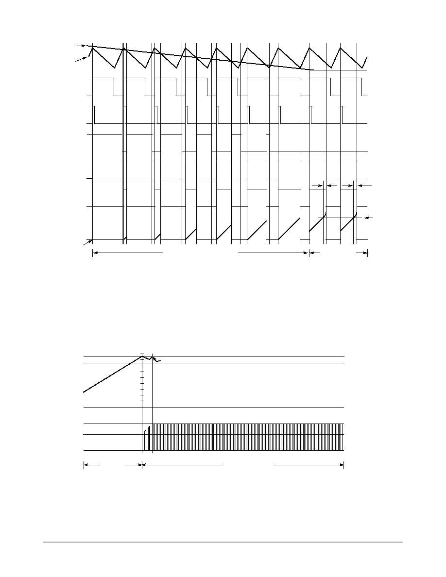
PWM Comparator and Latch
The pulse width modulator (PWM) consists of a
comparator with the Oscillator ramp output applied to the
inverting input. The Oscillator clock output applies a set
pulse to the PWM Latch when the timing capacitor reaches
its peak voltage, initiating Power Switch Circuit conduction.
As the timing capacitor discharges, the ramp voltage
decreases to a level that is less than the Error Amplifier
output, causing the PWM Comparator to reset the latch and
terminate Power Switch Circuit conduction for the duration
of the ramp-down period. This method of having the
Oscillator set and the PWM Comparator reset the Latch
prevents the possibility of multiple output pulses during a
given Oscillator clock cycle. This circuit configuration is
commonly referred to as double pulse suppression logic. A
timing diagram is shown in Figure 18 that illustrates the
behavior of the pulse width modulator.
No load operation. The pulse width modulator is designed
to operate between 73% and 0% duty cycle. The ability to
operate down to zero duty cycle allows for no load operation
without the burden of preloads. This feature is consistent
with the Blue Angle requirements, as it minimizes power
consumption while in the stand-by operation mode. For
operation at no load, the output may skip cycles. This is a
common occurrence for this type of control circuit. The
converter will switch for several cycles, and due to delays in
the output filter and feedback loop, the duty cycle will not
be reduced until the output has exceeded it's regulation limit.
The unit will then shut down for several cycles until the
voltage is below the regulation limit, and then it will switch
again. During the time that switching cycles are not present
the output voltage will decay according to it's RC time
constant, which is based on the output capacitance and
internal loading from the regulation circuitry. During this
interval, the voltage on the V
CC
supply will also decay. If it
decays below the lower hysteretic turn off threshold, the unit
will shut down and recycle. This mode of operation is not
normally desirable. In order to avoid it, the time constant
for the V
CC
cap and load should be equal to, or greater
than the time constant of the output. If no load operation
is not required, a relatively small value (
t10 mF) for the
V
CC
capacitor is acceptable.
Feedback Input
The feedback input, pin 2, accepts the DC error signal that
feeds the non-inverting input to the PWM. Pin 2 has a
nominal 2.7 k
W internal resistor to ground, which converts
the optocoupler current into a voltage. Its' signal is filtered
by a 7.0 kHz low pass filter which reduces high frequency
noise to the input of the PWM comparator.
Typically, the photo transistor of the optocoupler is
connected between V
CC
(pin 1) and the Feedback input
(pin 2). The photo transistor is effectively a current source
which is driven by the LED, which is connected to the output
regulation circuit of the power supply. An external capacitor
may be connected from pin 2 to ground for additional noise
filtering if necessary.
When the feedback input is below the lower threshold of
the ramp signal, the output of the power converter will be
operating at full duty cycle. The input current vs. duty cycle
transfer function is shown in Figure 2. As the voltage
increases, the duty cycle will vary linearly with the change
in voltage at the feedback input, between the upper and
lower extremes of the ramp waveform 2.7 V to 4.1 volts.
Above the upper extreme point of the ramp, the duty cycle
will be zero and no power will be transmitted to the output.
The circuit should be designed such that when the output
is low, the optocoupler will be off, leaving the voltage at
pin 2 at ground (full duty cycle). As the output voltage
increases, the optocoupler will begin to conduct, such that
the voltage at pin 2 increases until the proper duty cycle is
reached to maintain regulation.
Pin 2 is protected from ESD transients by a 10 volt Zener
diode to ground.

NCP1000, NCP1001, NCP1002
http://onsemi.com
9
Current Limit Comparator and Power Switch Circuit
The NCP1000 series uses cycle-by-cycle current limiting
as a means of protecting the output switch transistor from
overstress. Current limiting is implemented by monitoring
the instantaneous output switch current during conduction,
and upon sensing an overcurrent condition, immediately
turning off the switch for the duration of the Oscillator
ramp-down period.
The Power Switch Circuit is constructed using a
SENSEFET
t allowing a virtually lossless method of
monitoring the drain current. A small number of the power
MOSFET cells are used for current sensing by connecting
their individual sources to a single ground referenced sense
resistor, R
pk
. The current limit comparator detects if the
voltage across R
pk
exceeds the reference level that is present
at the noninverting input. If exceeded, the comparator
quickly resets the PWM Latch, thus protecting the Power
Switch Circuit. Figure 9 shows that this detection method
yields a relatively constant current limit threshold over
temperature. The high voltage Power Switch Circuit is
integrated with the control logic circuitry and is designed to
directly drive the converter transformer. The Power Switch
Circuit is capable of switching 700 V with an associated
drain current that ranges from 0.5 A to 1.5 A. Proper drain
voltage snubbing during converter start-up and overload is
mandatory for reliable device operation.
A Leading Edge Blanking circuit was placed in the current
sensing signal path to prevent a premature reset of the PWM
Latch. A potential premature reset signal is generated each
time the Power Switch Circuit is driven into conduction and
appears as a narrow voltage spike across current sense
resistor R
pk
. The spike is due to the MOSFET gate to source
capacitance, transformer interwinding capacitance, and
output rectifier recovery time. The Leading Edge Blanking
circuit has a dynamic behavior that masks the current signal
until the Power Switch Circuit turn-on transition is
completed.
The current limit propagation delay time is typically
220 ns. This time is measured from when an overcurrent
appears at the Power Switch Circuit drain, to the beginning
of turn-off. Care must be taken during transformer
saturation so that the maximum device current limit rating
is not exceeded. To determine the peak Power Switch Circuit
current at turn off, the effect of the propagation delay must
be taken into account. To do this, use the appropriate Current
Limit Threshold value from the electrical tables, and then
add the
DIpk based on the di/dt from Figure 16. The di/dt of
the circuit can be calculated by the following formula:
di dt (A
m
s)
+
V L
where:
V is the rectified, filtered input voltage (volts)
L is the primary inductance of the flyback transformer
(Henries)
High Voltage Start-Up
The NCP1000-1002 contain an internal start-up circuit
that eliminates the need for external start-up components. In
addition, this circuit increases the efficiency of the supply as
it uses no power when in the normal mode of operation, but
instead uses the power supplied by the auxiliary winding.
Rectified, filtered ac line voltage is connected to pin 4. An
internal JFET allows current to flow from the start-up pin,
to the V
CC
pin at a current of approximately 3.0 mA.
Figure 5 shows the startup current out of pin 1 which charges
the capacitor(s) connected to this pin.
The start circuit will be enhanced (conducting) when the
voltage at Pin 1 (V
CC
) is less than 7.5 volts. It will remain
enhanced until the V
CC
voltage reaches 8.5 volts. At this
point the Power Switch Circuit will be disabled, and the unit
will generate voltage via the auxiliary winding to maintain
proper operation of the device. Figure 4 shows the charge
time for turn-on vs. V
CC
capacitance when the unit is
initially energized.
If the V
CC
voltage drops below 7.5 volts (e.g. current limit
mode), the start circuit will again begin conducting, and will
charge up the V
CC
cap until the 8.5 volt limit is reached.
V
CC
Limiter and Undervoltage Lockout
The undervoltage lockout (UVLO) is designed to
guarantee
that the integrated circuit has sufficient voltage to
be fully functional before the output stage is enabled. It
inhibits operation of the major functions of the device by
disabling the Internal Bias circuitry, and assures that the
Power Switch Circuit remains in its "off'' state as the bias
voltage is initially brought up from zero volts. When the
NCP100x is in the "off'' state, the High Voltage Start-up
circuit is operational. The UVLO is a hysteretic switch and
will hold the device in its "off'' state any time that the V
CC
voltage is less than 7.5 volts. As the V
CC
increases past 7.5
volts, the NCP100x will remain off until the upper threshold
of 8.6 volts is reached. At this time the power converter is
enabled and will commence operation. The UVLO will
allow the unit to continue to operate as long as the V
CC
voltage exceeds 7.5 volts. The temperature characteristics of
the UVLO circuit are shown in Figure 8.
If the converter output is overloaded or shorted, the device
will enter the auto restart mode. This happens when the
auxiliary winding of the power transformer does not have
sufficient voltage to support the V
CC
requirements of the
chip. Once the chip is operational, if the V
CC
voltage falls
below 7.5 volts the unit will shut down, and the High Voltage
Start-up circuit will be enabled. This will charge the V
CC
cap up to 8.5 volts, which will clock the divide by eight
counter. The divide by eight counter holds the Power Switch
Circuit off. This causes the V
CC
cap to discharge. It will
continue to discharge and recharge for eight consecutive
cycles. After the eighth cycle, the unit will turn on again. If
the fault remains, the unit will again cycle through the auto
restart mode; if the fault has cleared the unit will begin
normal operation. The auto restart mode greatly reduces the
power dissipation of the power devices in the circuit and

NCP1000, NCP1001, NCP1002
http://onsemi.com
10
improves reliability in overload conditions. Figure 20 shows
the timing waveforms in auto restart mode.
The V
CC
pin receives its start-up power from the high
voltage start-up circuit. Once the undervoltage lockout trip
point is exceeded, the high voltage start-up circuit turns off,
and the V
CC
pin receives its power from the auxiliary
winding of the power transformer. Once the converter is
enabled, the V
CC
voltage will be clamped by the 8.6 volt
limiter. Since the voltage limiter will regulate the V
CC
voltage at 8.6 volts, it must shunt all excess current based on
the input impedance to this pin. A resistor is required
between the auxiliary winding filter capacitor and the V
CC
pin to limit the current.
Optocoupler Fail-safe Circuit
The NCP100x has the ability to sense an open optocoupler
and protect the load in the event of a failure. This circuit
operates by sensing the current in the V
CC
limiter, and
detecting a high current which is an indication of an open
optocoupler.
The V
CC
pin receives the output of a current source which
is created by the voltage drop between the auxiliary winding
and the V
CC
limiter across the shunt resistor. The Vcc limiter
will clamp the V
CC
voltage to approximately 8.6 volts. Any
current that is available at this pin, that is not needed for
either the chip bias current, or the opto current is shunted
through this limiter.
The opto fail-safe circuit operates on the premise that
under an open opto condition, the opto current will all be
shunted through the V
CC
limiter, and the output voltage (and
therefore the auxiliary winding voltage) will increase. The
increase in auxiliary winding voltage will cause an
amplified increase in the current into the V
CC
pin. To detect
an open opto condition, the current in the limiter is measured
and if it exceeds 10 milliamps, the chip will shut down and
go into burst mode operation. After a shutdown signal, the
optocoupler fail-safe circuit will enable the
divide-by-eight counter and attempt to restart the unit after
every eight V
CC
cycles.
For this circuit to operate properly, the shunt resistor must
be chosen prudently. There is a range of values for R
S
that
will determine the operation of this circuit. On one extreme,
a large value of R
S
will minimize the bias current, which will
have the effect of maximizing efficiency, while reducing the
response to an open optocoupler. The other extreme is the
minimum value of R
S,
which will maximize the bias current
into the chip and minimize the voltage overshoot in the event
of an open optocoupler
.
For minimum bias current:
Rsmax
+
(V
AUX min
*
8.8 volts)
I
CC1max
where:
V
AUXmin
is the minimum expected DC voltage from the
auxiliary winding.
Typically, this voltage will vary between
"5% to "10%
from it's nominal value.
I
CC1max
is the maximum rated bias current for the device
used. This value can found in the tables on the data sheet.
For the best optocoupler fail-safe response:
Rs
min
+
(V
AUX max
*
7.2 volts)
1.0mA
)
I
trip
where:
V
AUXmax
is the maximum expected DC voltage from the
auxiliary winding.
I
trip
is the minimum trip current for the optocoupler
fail- safe. This information can be found in the tables under
Current Limit and Thermal Protection, as well as in
Figure 12.
The value of R
S
that is used in the circuit must be between
the two extreme values calculated. Setting it closer to R
Smin
will optimize the optocoupler fail-safe feature, while setting
it closer to the R
Smax
value will minimize the bias current
Thermal Shutdown and Package
The internal Thermal Shutdown block protects the device
in the event that the maximum junction temperature is
exceeded. When activated, typically at 140
∞
C, one input of
the Driver is held low to disable the Power Switch Circuit.
Thermal shutdown activation is non-latching and the Power
Switch Circuit is allowed resume operation when the
junction temperature falls below 110
∞
C. The thermal
shutdown feature is provided to prevent catastrophic device
failures from accidental overheating. It is not intended to be
used as a substitute for proper heatsinking.
The die in the 8-pin dual-in-line package is mounted on
a special heat tab copper alloy lead frame. The tab consists
of pins 3, 6, 7, 8 is specifically designed to improve the
thermal conduction from the die to the printed circuit board.
This permits the use of standard layout and mounting
practices while having the ability to halve the junction to air
thermal resistance.
The die in the 5-pin TO-220 style package is mounted
directly on a copper alloy heat tab. This metal tab is exposed
on the backside of the package for heatsink attachment and
is electrically common to the device ground, Pin 3. A wide
variety of TO-220 style heatsinks are commercially
available for enhancing the thermal performance and
converter output power capability.

NCP1000, NCP1001, NCP1002
http://onsemi.com
11
Applications
The TO-220 devices have a single Ground, pin 3, that
serves the high current return path for the Power Switch
Circuit. Do not attempt to construct a converter circuit
on a wire-wrap or plug-in prototype board. In order to
ensure proper device operation and stability, it is important
to minimize the lead length and the associated inductance of
the ground pin. This pin must connect as directly as possible
to the printed circuit ground plane and should not be bent or
offset by the board layout. The Power Switch Circuit pin can
be offset if additional layout creepage distance is required.
Due to the potentially high rate of change in switch current,
a capacitor (if used), at pin 2, should have traces as short as
possible, from pin 2 and ground. This will significantly
reduce the level of switching noise that can be imposed upon
the feedback control signal.
Thermal
Shutdown
Figure 17. Representative Block Diagram
Snubber
Feedback
Input
R
pk
Power Switch
Circuit
+
+
+
+
-
Converter
DC Output
2
4
AC Line
Input
1
Internal
Bias
State Control
Power up-reset
Ck
R
Divide
by 8
S
R
Q
PWM Latch
Leading Edge
Blanking
Undervoltage
Lockout
Driver
10 V
Oscillator
Duty Cycle
Ramp
Clock
PWM
Comparator
7.0 kHz
Filter
Loop Compensation
Ground
3
Start-Up
+
Auxiliary Output
5
Auto Restart Timing
V
CC
Limiter 8.6 V
+
2.7 k
+
+
V
CC
Q
Start-Up
Current Limit
Comparator
10 V
10 mA
Opto Fail-safe
8.5 V/
7.5 V
Bypass
NCP1000, NCP1001, NCP1002
http://onsemi.com
12
Figure 18. Pulse Width Modulation Timing Diagram
Normal PWM Operating Range
Output Overload
Leading Edge
Blanking Input
(Power Switch
Circuit Current)
Power Switch
Circuit Gate Drive
PWM Latch
Q Output
PWM
Comparator
Output
Oscillator Clock
Oscillator
Duty Cycle
Oscillator Ramp
Feedback Input
(R
fb
Voltage)
Current Limit
Propagation
Delay
Current
Limit
Threshold
Zero Duty Cycle
Figure 19. Start-up and Normal Operation Timing Diagram
8.6 V
7.5 V
0 V
0 V
Flyback Voltage
Rectified Line Voltage
Switching
Regulation Threshold
V
CC
Limiter
(Pin 1)
Power Switch
Circuit Voltage
(Pin 5)
Switching Disabled
Normal Operation
Start-up

NCP1000, NCP1001, NCP1002
http://onsemi.com
13
Hysteretic Regulation
Figure 20. Auto Restart Operation Timing Diagram
8.6 V
7.5 V
0 V
0 V
Flyback Voltage
Rectified Line Voltage
Switching
V
CC
Limiter
(Pin 1)
Power Switch
Circuit Voltage
(Pin 5)
Switching Disabled
Auto Restart Operation with Overloaded or Shorted Output
Start-up
Start-Up MOSFET
Duty Cycle
During Auto Restart
35%
65%
Switching
Switching Disabled
Switching
Switching Disabled
Start-Up Circuit
On
I
start
Off
I
CC1
On
I
start
Off
I
CC2
On
I
start
Off
I
CC2
On
I
start
Off
I
CC1
Eight Cycles
1
2
7
8
1
7
2
8
1
5%
Power Switch Circuit Duty Cycle During Auto Restart
95%

NCP1000, NCP1001, NCP1002
http://onsemi.com
14
APPLICATIONS INFORMATION
APPLICATION #1: Offline Converter Provides
5.0 Volt, 1.0 Amp Output for Small Electronic
Equipment
ON Semiconductor's NCP1000 series of offline
converters offers a low cost, high efficiency power source
for low power, electronic equipment. It serves the same
function as small, line frequency transformers, but with the
added benefits of line and load regulation, transient
suppression, reduction in weight, and operation across the
universal input voltage range.
This kit provides a 5.0 volt, 1.0 amp output, which is
derived from an input source of 85 to 265 Vac, and 50 Hz to
60 Hz. This range of input voltages will allow this circuit to
function virtually anywhere in the world without
modification. The output is regulated and current limited,
and EMI filters are included on both the input and output.
Converter Test Data
Parameter
Conditions
Data
Line Regulation
85 v
v
Vin
v
265 v
D
Vo = 6.0 mV
Load Regulation
0 A
v
lo
v
1.0 A
D
Vo = 8.0 mV
Combined Line/
Load Regulation
85 v
v
Vin
v
265 v
.09 A
v
lo
v
1.0 A
D
Vo = 10 mV
Output Ripple
lo = 1.0 A
100 mV
pp
Input Power
V
in
= 115 v, lo = 1.0 A
V
in
= 220 v, lo = 1.0 A
7.75 watts
7.88 watts
Power Factor
V
in
= 115 v, lo = 1.0 A
V
in
= 220 v, lo = 1.0 A
-.57
-.49
Efficiency
V
in
= 115 v, lo = 1.0 A
V
in
= 220 v, lo = 1.0 A
h
= 66%
h
= 64%
C2a C2b
RS
6.8
6.8
R7
+
+
C3
R2
C8
D6
R1
C5
C1
C4
p/o U2
D5
C6
C7
R3
C10
R4
p/o U2
C9
5 V, 1 A
RETURN
1
L2
NCP
Vin
F1
D1 - D4
U3
R5
1000
Figure 21. Wall Adapter Schematic
For additional information on this application, please order application note AND8019/D from the Literature Distribution Center or download
from our website at http://onsemi.com.

NCP1000, NCP1001, NCP1002
http://onsemi.com
15
PACKAGE DIMENSIONS
TO-220
T SUFFIX
CASE 314P-01
ISSUE O
DIP-8
P SUFFIX
CASE 626-05
ISSUE L
NOTES:
1. DIMENSION L TO CENTER OF LEAD WHEN
FORMED PARALLEL.
2. PACKAGE CONTOUR OPTIONAL (ROUND OR
SQUARE CORNERS).
3. DIMENSIONING AND TOLERANCING PER ANSI
Y14.5M, 1982.
1
4
5
8
F
NOTE 2
-A-
-B-
-T-
SEATING
PLANE
H
J
G
D
K
N
C
L
M
M
A
M
0.13 (0.005)
B
M
T
DIM
MIN
MAX
MIN
MAX
INCHES
MILLIMETERS
A
9.40
10.16
0.370
0.400
B
6.10
6.60
0.240
0.260
C
3.94
4.45
0.155
0.175
D
0.38
0.51
0.015
0.020
F
1.02
1.78
0.040
0.070
G
2.54 BSC
0.100 BSC
H
0.76
1.27
0.030
0.050
J
0.20
0.30
0.008
0.012
K
2.92
3.43
0.115
0.135
L
7.62 BSC
0.300 BSC
M
---
10
---
10
N
0.76
1.01
0.030
0.040
_
_
-Q-
1 2 3 4 5
U
K
D
G
A
B
5 PL
J
H
L
E
C
M
Q
M
0.356 (0.014)
T
SEATING
PLANE
-T-
DIM
MIN
MAX
MIN
MAX
MILLIMETERS
INCHES
A
0.572
0.613
14.529
15.570
B
0.390
0.415
9.906
10.541
C
0.165
0.187
4.191
4.750
D
0.025
0.038
0.635
0.965
E
0.045
0.055
1.143
1.397
G
0.067 BSC
1.702 BSC
H
0.087
0.112
2.210
2.845
J
0.015
0.025
0.381
0.635
K
0.990
1.045
25.146
26.543
L
0.320
0.365
8.128
9.271
Q
0.140
0.156
3.556
3.962
U
0.105
0.117
2.667
2.972
NOTES:
1. DIMENSIONING AND TOLERANCING PER ANSI
Y14.5M, 1982.
2. CONTROLLING DIMENSION: INCH.
3. DIMENSION D DOES NOT INCLUDE
INTERCONNECT BAR (DAMBAR) PROTRUSION.
DIMENSION D INCLUDING PROTRUSION SHALL
NOT EXCEED 10.92 (0.043) MAXIMUM.

NCP1000, NCP1001, NCP1002
http://onsemi.com
16
ON Semiconductor and are registered trademarks of Semiconductor Components Industries, LLC (SCILLC). SCILLC reserves the right to make
changes without further notice to any products herein. SCILLC makes no warranty, representation or guarantee regarding the suitability of its products for any
particular purpose, nor does SCILLC assume any liability arising out of the application or use of any product or circuit, and specifically disclaims any and all
liability, including without limitation special, consequential or incidental damages. "Typical" parameters which may be provided in SCILLC data sheets and/or
specifications can and do vary in different applications and actual performance may vary over time. All operating parameters, including "Typicals" must be
validated for each customer application by customer's technical experts. SCILLC does not convey any license under its patent rights nor the rights of others.
SCILLC products are not designed, intended, or authorized for use as components in systems intended for surgical implant into the body, or other applications
intended to support or sustain life, or for any other application in which the failure of the SCILLC product could create a situation where personal injury or death
may occur. Should Buyer purchase or use SCILLC products for any such unintended or unauthorized application, Buyer shall indemnify and hold SCILLC
and its officers, employees, subsidiaries, affiliates, and distributors harmless against all claims, costs, damages, and expenses, and reasonable attorney fees
arising out of, directly or indirectly, any claim of personal injury or death associated with such unintended or unauthorized use, even if such claim alleges that
SCILLC was negligent regarding the design or manufacture of the part. SCILLC is an Equal Opportunity/Affirmative Action Employer.
PUBLICATION ORDERING INFORMATION
JAPAN: ON Semiconductor, Japan Customer Focus Center
2-9-1 Kamimeguro, Meguro-ku, Tokyo, Japan 153-0051
Phone: 81-3-5773-3850
ON Semiconductor Website: http://onsemi.com
For additional information, please contact your local
Sales Representative.
NCP1000/D
The products described herein (NCP1000, 1001, 1002), may be covered by one or more of the following U.S. patents: 4,553,084;
5,418,410; 5,477,175; 5,760,639; 5,859,768. There may be other patents pending.
SENSEFET is a trademark of Semiconductor Components Industries, LLC (SCILLC)
Literature Fulfillment:
Literature Distribution Center for ON Semiconductor
P.O. Box 5163, Denver, Colorado 80217 USA
Phone: 303-675-2175 or 800-344-3860 Toll Free USA/Canada
Fax: 303-675-2176 or 800-344-3867 Toll Free USA/Canada
Email: ONlit@hibbertco.com
N. American Technical Support: 800-282-9855 Toll Free USA/Canada