©
Semiconductor Components Industries, LLC, 2004
September, 2004 - Rev. 10
1
Publication Order Number:
NCP1010/D
NCP1010, NCP1011,
NCP1012, NCP1013,
NCP1014
Self-Supplied Monolithic
Switcher for Low Standby-
Power Offline SMPS
The NCP101X series integrates a fixed-frequency current-mode
controller and a 700 V MOSFET. Housed in a PDIP-7,
PDIP-7 Gull Wing, or SOT-223 package, the NCP101X offers
everything needed to build a rugged and low-cost power supply,
including soft-start, frequency jittering, short-circuit protection,
skip-cycle, a maximum peak current setpoint and a Dynamic
Self-Supply (no need for an auxiliary winding).
Unlike other monolithic solutions, the NCP101X is quiet by nature:
during nominal load operation, the part switches at one of the available
frequencies (65 - 100 - 130 kHz). When the current setpoint falls
below a given value, e.g. the output power demand diminishes, the IC
automatically enters the so-called skip-cycle mode and provides
excellent efficiency at light loads. Because this occurs at typically 1/4
of the maximum peak value, no acoustic noise takes place. As a result,
standby power is reduced to the minimum without acoustic noise
generation.
Short-circuit detection takes place when the feedback signal fades
away, e.g. in true short-circuit conditions or in broken Optocoupler
cases. External disabling is easily done either simply by pulling the
feedback pin down or latching it to ground through an inexpensive
SCR for complete latched-off. Finally soft-start and frequency
jittering further ease the designer task to quickly develop low-cost and
robust offline power supplies.
For improved standby performance, the connection of an auxiliary
winding stops the DSS operation and helps to consume less than
100 mW at high line. In this mode, a built-in latched overvoltage
protection prevents from lethal voltage runaways in case the
Optocoupler would brake. These devices are available in economical
8-pin dual-in-line and 4-pin SOT-223 packages.
Features
∑
Built-in 700 V MOSFET with Typical R
DSon
of 11
W
and 22
W
∑
Large Creepage Distance Between High-Voltage Pins
∑
Current-Mode Fixed Frequency Operation:
65 kHz ≠ 100 kHz - 130 kHz
∑
Skip-Cycle Operation at Low Peak Currents Only:
No Acoustic Noise!
∑
Dynamic Self-Supply, No Need for an Auxiliary
Winding
∑
Internal 1.0 ms Soft-Start
∑
Latched Overvoltage Protection with Auxiliary
Winding Operation
∑
Frequency Jittering for Better EMI Signature
∑
Auto-Recovery Internal Output Short-Circuit
Protection
∑
Below 100 mW Standby Power if Auxiliary Winding
is Used
∑
Internal Temperature Shutdown
∑
Direct Optocoupler Connection
∑
SPICE Models Available for TRANsient Analysis
∑
Pb-Free Packages are Available*
Typical Applications
∑
Low Power AC/DC Adapters for Chargers
∑
Auxiliary Power Supplies (USB, Appliances,
TVs, etc.)
*For additional information on our Pb-Free strategy and soldering details, please download the ON Semiconductor Soldering and Mounting
Techniques Reference Manual, SOLDERRM/D.
PDIP-7
CASE 626A
AP SUFFIX
1
8
MARKING DIAGRAMS
P101xAPyy
AWL
YYWW
1
See detailed ordering and shipping information in the package
dimensions section on page 22 of this data sheet.
ORDERING INFORMATION
SOT-223
CASE 318E
ST SUFFIX
1
4
101xy
ALYW
1
4
x
= Current Limit (0, 1, 2, 3, 4)
yy
= 06 (65 kHz), 10 (100 kHz), 13 (130 kHz)
y
= Oscillator Frequency
A (65 kHz), B (100 kHz), C (130 kHz)
A
= Assembly Location
WL, L
= Wafer Lot
YY, Y
= Year
WW, W = Work Week
http://onsemi.com
1
PDIP-7
(Gull Wing)
CASE 626AA
APL SUFFIX
1
101xAPLyy
AWL
YYWW
NCP1010, NCP1011, NCP1012, NCP1013, NCP1014
http://onsemi.com
2
1
V
CC
8 GND
2
NC
3
NC
4
FB
7 NC
5 DRAIN
(Top View)
PIN CONNECTIONS
PDIP-7
SOT-223
(Top View)
1
2
3
4
V
CC
FB
DRAIN
GND
1
V
CC
8 GND
2
NC
3
NC
4
FB
7 NC
5 DRAIN
(Top View)
PDIP-7
(Gull Wing)
Indicative Maximum Output Power from NCP1014
R
DSon
- Ip
230 Vac
100 - 250 Vac
11
W
- 450 mA DSS
14 W
6.0 W
11
W
- 450 mA Auxiliary Winding
19 W
8.0 W
1. Informative values only, with: Tamb = 50
∞
C, Fswitching = 65 kHz, circuit mounted on minimum copper area as recommended.
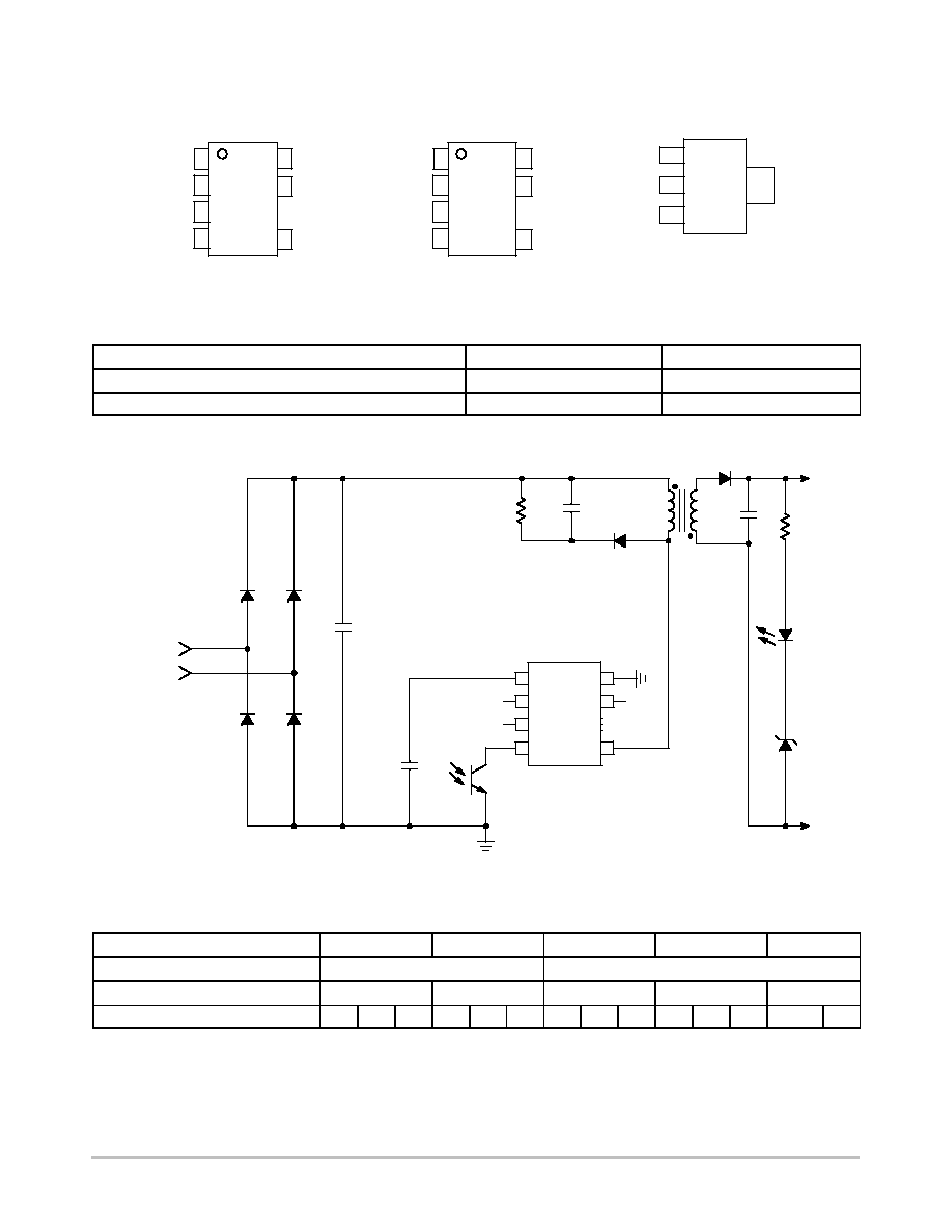
Figure 1. Typical Application Example
2
7
3
4
5
1
8
100-250 Vac
+
+
NCP101X
Vout
+
GND
Quick Selection Table
NCP1010
NCP1011
NCP1012
NCP1013
NCP1014
R
DSon
[
W
]
22
11
Ipeak [mA]
100
250
250
350
450
Freq [kHz]
65
100
130
65
100
130
65
100
130
65
100
130
65
100
NCP1010, NCP1011, NCP1012, NCP1013, NCP1014
http://onsemi.com
3
PIN FUNCTION DESCRIPTION
Pin No.
(SOT-223)
Pin No.
(PDIP-7,
PDIP-7/Gull Wing)
Pin Name
Function
Description
1
1
V
CC
Powers the Internal Circuitry
This pin is connected to an external capacitor of typi-
cally 10
m
F. The natural ripple superimposed on the
V
CC
participates to the frequency jittering. For im-
proved standby performance, an auxiliary V
CC
can be
connected to Pin 1. The V
CC
also includes an active
shunt which serves as an opto fail-safe protection.
-
2
NC
-
-
-
3
NC
-
-
2
4
FB
Feedback Signal Input
By connecting an optocoupler to this pin, the peak
current setpoint is adjusted accordingly to the output
power demand.
3
5
Drain
Drain Connection
The internal drain MOSFET connection.
-
-
-
-
-
-
7
NC
-
This unconnected pin ensures adequate creepage
distance.
4
8
GND
The IC Ground
-
65, 100 or
130 kHz
Clock
Overload?
UVLO
Management
NC
NC
V
CC
FB
Drain
NC
GND
Figure 2. Simplified Internal Circuit Architecture
2
1
3
4
IV
CC
I?
Vclamp*
4 V
18 k
Error flag armed?
EMI Jittering
V
CC
Startup Source
Drain
Flip-Flop
DCmax = 65%
Reset
Reset
High when V
CC
t
3 V
Driver
S
Q
R
-
+
Iref = 7.4 mA
IV
CC
Set
Q
V
CC
8
Rsense
250 ns
L.E.B.
7
5
-
+
+
-
Soft-Start
Startup Sequence
Overload
- +
0.5 V
Drain
*Vclamp = VCC
OFF
+ 200 mV (8.7 V Typical)

NCP1010, NCP1011, NCP1012, NCP1013, NCP1014
http://onsemi.com
4
¡¡¡¡¡¡¡¡¡¡¡¡¡¡¡¡¡¡¡¡¡¡¡¡¡¡¡¡¡¡¡¡¡
¡¡¡¡¡¡¡¡¡¡¡¡¡¡¡¡¡¡¡¡¡¡¡¡¡¡¡¡¡¡¡¡¡
MAXIMUM RATINGS
¡¡¡¡¡¡¡¡¡¡¡¡¡¡¡¡¡¡¡¡¡
¡¡¡¡¡¡¡¡¡¡¡¡¡¡¡¡¡¡¡¡¡
Rating
¡¡¡¡¡
¡¡¡¡¡
Symbol
¡¡¡¡¡¡
¡¡¡¡¡¡
Value
¡¡¡¡
¡¡¡¡
Unit
Power Supply Voltage on all pins, except Pin 5 (Drain)
V
CC
-0.3 to 10
V
Drain Voltage
-
-0.3 to 700
V
Drain Current Peak during Transformer Saturation
I
DS(pk)
2 x I
lim
max
A
Maximum Current into Pin 1 when Activating the 8.7 V Active Clamp
I_V
CC
15
mA
Thermal Characteristics
P Suffix, Case 626A and PL Suffix (Gull Wing), Case 626AA
Junction-to-Lead
Junction-to-Air, 2.0 oz Printed Circuit Copper Clad
0.36 Sq. Inch
1.0 Sq. Inch
ST Suffix, Plastic Package Case 318E
Junction-to-Lead
Junction-to-Air, 2.0 oz Printed Circuit Copper Clad
0.36 Sq. Inch
1.0 Sq. Inch
R
q
JL
R
q
JA
R
q
JL
R
q
JA
9.0
77
60
14
74
55
∞
C/W
Maximum Junction Temperature
T
Jmax
150
∞
C
Storage Temperature Range
-
-60 to +150
∞
C
ESD Capability, Human Body Model (All pins except HV)
-
2.0
kV
ESD Capability, Machine Model
-
200
V
Maximum ratings are those values beyond which device damage can occur. Maximum ratings applied to the device are individual stress limit
values (not normal operating conditions) and are not valid simultaneously. If these limits are exceeded, device functional operation is not implied,
damage may occur and reliability may be affected.

NCP1010, NCP1011, NCP1012, NCP1013, NCP1014
http://onsemi.com
5
ELECTRICAL CHARACTERISTICS
(For typical values T
J
= 25
∞
C, for min/max values T
J
= 0
∞
C to +125
∞
C, Max T
J
= 150
∞
C,
V
CC
= 8.0 V unless otherwise noted.)
Rating
Pin
Symbol
Min
Typ
Max
Unit
SUPPLY SECTION AND V
CC
MANAGEMENT
V
CC
Increasing Level at which the Current Source Turns-off
1
VCC
OFF
7.9
8.5
9.1
V
V
CC
Decreasing Level at which the Current Source Turns-on
1
VCC
ON
6.9
7.5
8.1
V
V
CC
Decreasing Level at which the Latch-off Phase Ends
1
VCC
latch
4.4
4.7
5.1
V
V
CC
Decreasing Level at which the Internal Latch is Released
1
VCC
reset
-
3.0
-
V
Internal IC Consumption, MOSFET Switching at 65 kHz
1
ICC1
-
0.92
1.1
(Note 2)
mA
Internal IC Consumption, MOSFET Switching at 100 kHz
1
ICC1
-
0.95
1.15
(Note 2)
mA
Internal IC Consumption, MOSFET Switching at 130 kHz
1
ICC1
-
0.98
1.2
(Note 2)
mA
Internal IC Consumption, Latch-off Phase, V
CC
= 6.0 V
1
ICC2
-
290
-
m
A
Active Zener Voltage Positive Offset to VCC
OFF
1
Vclamp
140
200
300
mV
Latch-off Current
NCP1012/13/14
NCP1010/11
1
ILatch
6.3
5.8
7.4
7.3
9.2
9.0
mA
POWER SWITCH CIRCUIT
Power Switch Circuit On-state Resistance
NCP1012/13/14 (Id = 50 mA)
T
J
= 25
∞
C
T
J
= 125
∞
C
NCP1010/11 (Id = 50 mA)
T
J
= 25
∞
C
T
J
= 125
∞
C
5
R
DSon
-
11
19
22
38
16
24
35
50
W
Power Switch Circuit and Startup Breakdown Voltage
(ID
(off)
= 120
m
A, T
J
= 25
∞
C)
5
BVdss
700
-
-
V
Power Switch and Startup Breakdown Voltage Off-state
Leakage Current
T
J
= 25
∞
C (Vds = 700 V)
T
J
= 125
∞
C (Vds = 700 V)
5
5
I
DS(OFF
)
-
-
50
30
-
-
m
A
Switching Characteristics
(RL = 50
W
, Vds Set for Idrain = 0.7 x Ilim)
Turn-on Time (90%-10%)
Turn-off Time (10%-90%)
5
5
ton
toff
-
-
20
10
-
-
ns
INTERNAL STARTUP CURRENT SOURCE
High-voltage Current Source, V
CC
= 8.0 V
NCP1012/13/14
NCP1010/11
1
IC1
5.0
5.0
8.0
8.5
10
10.3
mA
High-voltage Current Source, V
CC
= 0
1
IC2
-
10
-
mA
CURRENT COMPARATOR T
J
= 25
∞
C (Note 2)
Maximum Internal Current Setpoint, NCP1010 (Note 3)
5
Ipeak (22)
90
100
110
mA
Maximum Internal Current Setpoint, NCP1011 (Note 3)
5
Ipeak (22)
225
250
275
mA
Maximum Internal Current Setpoint, NCP1012 (Note 3)
5
Ipeak (11)
225
250
275
mA
Maximum Internal Current Setpoint, NCP1013 (Note 3)
5
Ipeak (11)
315
350
385
mA
Maximum Internal Current Setpoint, NCP1014 (Note 3)
5
Ipeak (11)
405
450
495
mA
Default Internal Current Setpoint for Skip-Cycle Operation,
Percentage of Max Ip
-
I
Lskip
-
25
-
%
Propagation Delay from Current Detection to Drain OFF State
-
T
DEL
-
125
-
ns
Leading Edge Blanking Duration
-
T
LEB
-
250
-
ns
2. See characterization curves for temperature evolution.
3. Adjust di/dt to reach Ipeak in 3.2
m
sec.

NCP1010, NCP1011, NCP1012, NCP1013, NCP1014
http://onsemi.com
6
ELECTRICAL CHARACTERISTICS (continued)
(For typical values T
J
= 25
∞
C, for min/max values T
J
= 0
∞
C to +125
∞
C,
Max T
J
= 150
∞
C, V
CC
= 8.0 V unless otherwise noted.)
Rating
Pin
Symbol
Min
Typ
Max
Unit
INTERNAL OSCILLATOR
Oscillation Frequency, 65 kHz Version, T
J
= 25
∞
C (Note 4)
-
f
OSC
59
65
71
kHz
Oscillation Frequency, 100 kHz Version, T
J
= 25
∞
C (Note 4)
-
f
OSC
90
100
110
kHz
Oscillation Frequency, 130 kHz Version, T
J
= 25
∞
C (Note 4)
-
f
OSC
117
130
143
kHz
Frequency Dithering Compared to Switching Frequency
(with active DSS)
-
f
dither
-
"
3.3
-
%
Maximum Duty-cycle
-
Dmax
62
67
72
%
FEEDBACK SECTION
Internal Pull-up Resistor
4
Rup
-
18
-
k
W
Internal Soft-Start (Guaranteed by Design)
-
Tss
-
1.0
-
ms
SKIP-CYCLE GENERATION
Default Skip Mode Level on FB Pin
4
Vskip
-
0.5
-
V
TEMPERATURE MANAGEMENT
Temperature Shutdown
-
TSD
-
150
-
∞
C
Hysteresis in Shutdown
-
-
-
50
-
∞
C
4. See characterization curves for temperature evolution.

NCP1010, NCP1011, NCP1012, NCP1013, NCP1014
http://onsemi.com
7
TYPICAL CHARACTERISTICS
Figure 3. IC1 @ V
CC
= 8.0 V, FB = 1.5 V
vs. Temperature
-10.0
-9.0
-8.0
-7.0
-6.0
-5.0
-4.0
-3.0
-2.0
-25
0
25
50
75
100
125
TEMPERATURE (
∞
C)
IC1 ( mA)
Figure 4. ICC1 @ V
CC
= 8.0 V, FB = 1.5 V
vs. Temperature
0.50
0.60
0.70
0.80
0.90
1.00
1.10
1.20
1.30
1.40
1.50
-25
0
25
50
75
100
125
TEMPERATURE (
∞
C)
ICC1 (mA)
Figure 5. ICC2 @ V
CC
= 6.0 V, FB = Open
vs. Temperature
0.20
0.22
0.24
0.26
0.28
0.30
0.32
0.34
0.36
0.38
0.40
-25
0
25
50
75
100
125
TEMPERATURE (
∞
C)
ICC2 (mA)
Figure 6. V
CC
OFF, FB = 1.5 V vs.
Temperature
8.20
8.30
8.40
8.50
8.60
8.70
8.80
8.90
9.00
-25
0
25
50
75
100
125
TEMPERATURE (
∞
C)
VCC-OFF ( V )
Figure 7. V
CC
ON, FB = 3.5 V vs. Temperature
7.00
7.10
7.20
7.30
7.40
7.50
7.60
7.70
7.80
7.90
8.00
-25
0
25
50
75
100
125
TEMPERATURE (
∞
C)
VCC-ON ( V)
Figure 8. Duty Cycle vs. Temperature
65
66
66
67
67
68
68
-25
0
25
50
75
100
125
TEMPERATURE (
∞
C)
DUTY
CYCLE (%)

NCP1010, NCP1011, NCP1012, NCP1013, NCP1014
http://onsemi.com
8
TYPICAL CHARACTERISTICS
Figure 9. ILatch, FB = 1.5 V vs. Temperature
7.00
7.20
7.40
7.60
7.80
8.00
8.20
8.40
8.60
8.80
9.00
-25
0
25
50
75
100
125
TEMPERATURE (
∞
C)
I_Latch (mA)
Figure 10. Ipeak-RR, V
CC
= 8.0 V, FB = 3.5 V
vs. Temperature
300
320
340
360
380
400
420
440
460
480
500
-25
0
25
50
75
100
125
TEMPERATURE (
∞
C)
Ipeak (mA)
Figure 11. Frequency vs. Temperature
40
60
80
100
120
140
160
-25
0
25
50
75
100
125
TEMPERATURE (
∞
C)
100 kHz
130 kHz
Figure 12. ON Resistance vs. Temperature,
NCP1012/1013
0.00
5.00
10.00
15.00
20.00
25.00
-25
0
25
50
75
100
125
TEMPERATURE (
∞
C)
R
DSon
(
W
)
f
OS
C
(kHz)
NCP1013
NCP1010, NCP1011, NCP1012, NCP1013, NCP1014
http://onsemi.com
9
APPLICATION INFORMATION
Introduction
The NCP101X offers a complete current-mode control
solution (actually an enhanced NCP1200 controller section)
together with a high-voltage power MOSFET in a
monolithic structure. The component integrates everything
needed to build a rugged and low-cost Switch-Mode Power
Supply (SMPS) featuring low standby power. The Quick
Selection Table on Page 2, details the differences between
references, mainly peak current setpoints and operating
frequency.
No need for an auxiliary winding: ON Semiconductor
Very High Voltage Integrated Circuit technology lets you
supply the IC directly from the high-voltage DC rail. We call
it Dynamic Self-Supply (DSS). This solution simplifies the
transformer design and ensures a better control of the SMPS
in difficult output conditions, e.g. constant current
operations. However, for improved standby performance,
an auxiliary winding can be connected to the V
CC
pin to
disable the DSS operation.
Short-circuit protection: By permanently monitoring the
feedback line activity, the IC is able to detect the presence of
a short-circuit, immediately reducing the output power for
a total system protection. Once the short has disappeared, the
controller resumes and goes back to normal operation.
Fail-safe optocoupler and OVP: When an auxiliary
winding is connected to the V
CC
pin, the device stops its
internal Dynamic Self-Supply and takes its operating power
from the auxiliary winding. A 8.7 V active clamp is
connected between V
CC
and ground. In case the current
injected in this clamp exceeds a level of 7.4 mA (typical),
the controller immediately latches off and stays in this
position until V
CC
cycles down to 3.0 V (e.g. unplugging the
converter from the wall). By adjusting a limiting resistor in
series with the V
CC
terminal, it becomes possible to
implement an overvoltage protection function, latching off
the circuit in case of broken optocoupler or feedback loop
problems.
Low standby-power: If SMPS naturally exhibits a good
efficiency at nominal load, it begins to be less efficient when
the output power demand diminishes. By skipping unneeded
switching cycles, the NCP101X drastically reduces the
power wasted during light load conditions. An auxiliary
winding can further help decreasing the standby power to
extremely low levels by invalidating the DSS operation.
Typical measurements show results below 80 mW @
230 Vac for a typical 7.0 W universal power supply.
No acoustic noise while operating: Instead of skipping
cycles at high peak currents, the NCP101X waits until the
peak current demand falls below a fixed 1/4 of the maximum
limit. As a result, cycle skipping can take place without
having a singing transformer
...
You can thus select cheap
magnetic components free of noise problems.
SPICE model: A dedicated model to run transient
cycle-by-cycle simulations is available but also an
averaged version to help close the loop. Ready-to-use
templates can be downloaded in OrCAD's PSpice, and
INTUSOFT's IsSpice4 from ON Semiconductor web site,
NCP101X related section.
Dynamic Self-Supply
When the power supply is first powered from the mains
outlet, the internal current source (typically 8.0 mA) is
biased and charges up the V
CC
capacitor from the drain pin.
Once the voltage on this V
CC
capacitor reaches the VCC
OFF
level (typically 8.5 V), the current source turns off and
pulses are delivered by the output stage: the circuit is awake
and activates the power MOSFET. Figure 13 details the
internal circuitry.
Figure 13. The Current Source Regulates V
CC
by Introducing a Ripple
Vref OFF = 8.5 V
Vref ON = 7.5 V
Vref Latch = 4.7 V*
-
+
Internal Supply
+
Vref
VCC
OFF
+200 mV
(8.7 V Typ.)
V
CC
+
CV
CC
Startup Source
Drain
*In fault condition

NCP1010, NCP1011, NCP1012, NCP1013, NCP1014
http://onsemi.com
10
Figure 14. The Charge/Discharge Cycle Over a 10
m
F V
CC
Capacitor
Vcc
8.5 V
7.5 V
Device
Internally
Pulses
Startup Period
8.00
6.00
4.00
2.00
0
The protection burst duty-cycle can easily be computed
through the various timing events as portrayed by Figure 16.
Being loaded by the circuit consumption, the voltage on
the V
CC
capacitor goes down. When the DSS controller
detects that V
CC
has reached 7.5 V (VCC
ON
), it activates the
internal current source to bring V
CC
toward 8.5 V and stops
again: a cycle takes place whose low frequency depends on
the V
CC
capacitor and the IC consumption. A 1.0 V ripple
takes place on the V
CC
pin whose average value equals
(VCC
OFF
+ VCC
ON
)/2. Figure 14 portrays a typical
operation of the DSS.
As one can see, the V
CC
capacitor shall be dimensioned to
offer an adequate startup time, i.e. ensure regulation is
reached before V
CC
crosses 7.5 V (otherwise the part enters
the fault condition mode). If we know that
DV = 1.0 V
and ICC1 (max) is 1.1 mA (for instance we selected an 11
W
device switching at 65 kHz), then the V
CC
capacitor can
be calculated using:
C
w
ICC1 ∑ tstartup
D
V
(eq. 1)
. Let's
suppose that the SMPS needs 10 ms to startup, then we will
calculate C to offer a 15 ms period. As a result, C should be
greater than 20
mF thus the selection of a 33 mF/16 V
capacitor is appropriate.
Short Circuit Protection
The internal protection circuitry involves a patented
arrangement that permanently monitors the assertion of an
internal error flag. This error flag is, in fact, a signal that
instructs the controller that the internal maximum peak
current limit is reached. This naturally occurs during the
startup period (Vout is not stabilized to the target value) or
when the optocoupler LED is no longer biased, e.g. in a
short-circuit condition or when the feedback network is
broken. When the DSS normally operates, the logic checks
for the presence of the error flag every time V
CC
crosses
VCC
ON
. If the error flag is low (peak limit not active) then
the IC works normally. If the error signal is active, then the
NCP101X immediately stops the output pulses, reduces its
internal current consumption and does not allow the startup
source to activate: V
CC
drops toward ground until it reaches
the so-called latch-off level, where the current source
activates again to attempt a new restart. When the error is
gone, the IC automatically resumes its operation. If the
default is still there, the IC pulses during 8.5 V down to 7.5 V
and enters a new latch-off phase. The resulting burst
operation guarantees a low average power dissipation and
lets the SMPS sustain a permanent short-circuit. Figure 15
shows the corresponding diagram.
Figure 15. Simplified NCP101X Short-Circuit
Detection Circuitry
-
+
4 V
FB
Division
Max
Ip
Flag
V
CC
VCC
ON
Signal
To
Latch
Reset
Current Sense
Information
Clamp
Active?

NCP1010, NCP1011, NCP1012, NCP1013, NCP1014
http://onsemi.com
11
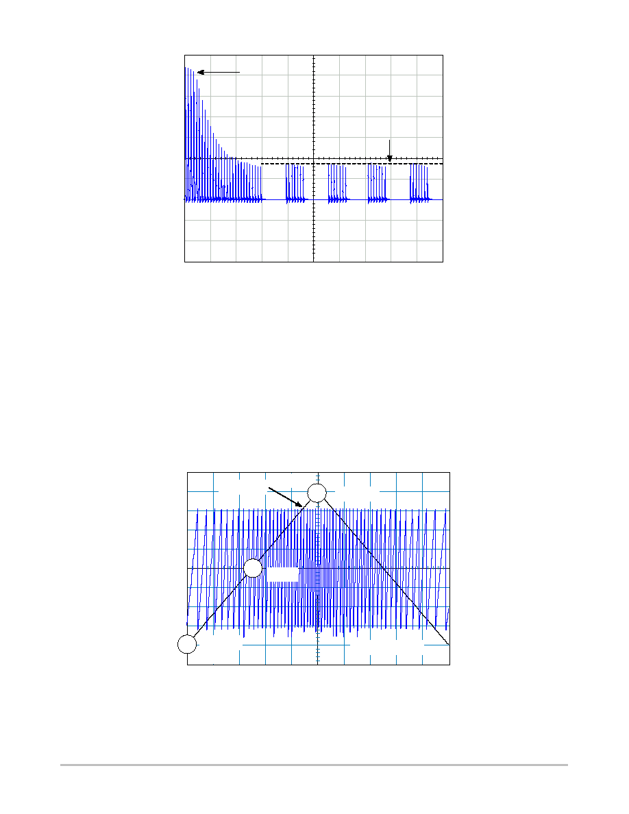
Figure 16. NCP101X Facing a Fault Condition (Vin = 150 Vdc)
Tstart
Tsw
TLatch
1 V Ripple
Latch-off
Level
The rising slope from the latch-off level up to 8.5 V
is expressed by:
Tstart
+ D
V1 ∑ C
IC1
. The time during which
the IC actually pulses is given by
tsw
+ D
V2 ∑ C
ICC1
.
Finally, the latch-off time can be derived
using the same formula topology:
TLatch
+ D
V3 ∑ C
ICC2
.
From these three definitions, the burst duty-cycle
can be computed:
dc
+
Tsw
Tstart
)
Tsw
)
TLatch
(eq. 2)
.
dc
+
D
V2
ICC1 ∑
D
V2
ICC1
)
D
V1
IC1
)
D
V3
ICC2
(eq. 3)
. Feeding the
equation with values extracted from the parameter section
gives a typical duty-cycle of 13%, precluding any lethal
thermal runaway while in a fault condition.
DSS Internal Dissipation
The Dynamic Self-Supplied pulls energy out from the
drain pin. In Flyback-based converters, this drain level can
easily go above 600 V peak and thus increase the stress on the
DSS startup source. However, the drain voltage evolves with
time and its period is small compared to that of the DSS. As
a result, the averaged dissipation, excluding capacitive losses,
can be derived by:
PDSS
+
ICC1 ∑
t
Vds(t)
u
.
(eq. 4)
.
Figure 17 portrays a typical drain-ground waveshape where
leakage effects have been removed.
Figure 17. A typical drain-ground waveshape
where leakage effects are not accounted for.
Vds(t)
Vin
Vr
toff
dt
ton
t
Tsw
By looking at Figure 17, the average result can easily be
derived by additive square area calculation:
t
Vds(t)
u+
Vin ∑ (1
*
d)
)
Vr ∑
toff
Tsw
(eq. 5)
By developing Equation 5, we obtain:
t
Vds(t)
u+
Vin
*
Vin ∑
ton
Tsw
)
Vr ∑
toff
Tsw
(eq. 6)
toff can be expressed by:
toff
+
Ip ∑
Lp
Vr
(eq. 7)
where ton
can be evaluated by:
ton
+
Ip ∑
Lp
Vin
(eq. 8)
.

NCP1010, NCP1011, NCP1012, NCP1013, NCP1014
http://onsemi.com
12
Plugging Equations 7 and 8 into Equation 6 leads to
t
Vds(t)
u+
Vin
and thus,
PDSS
+
Vin
ICC1
(eq. 9)
.
The worse case occurs at high line, when Vin equals
370 Vdc. With ICC1 = 1.1 mA (65 kHz version), we can
expect a DSS dissipation around 407 mW. If you select a
higher switching frequency version, the ICC1 increases and
it is likely that the DSS consumption exceeds that number.
In that case, we recommend to add an auxiliary winding in
order to offer more dissipation room to the power MOSFET.
Please read application note AND8125/D, "Evaluating
the Power Capability of the NCP101X Members" to help in
selecting the right part/configuration for your application.
Lowering the Standby Power with an Auxiliary Winding
The DSS operation can bother the designer when its
dissipation is too high and extremely low standby power is
a must. In both cases, one can connect an auxiliary winding
to disable the self-supply. The current source then ensures
the startup sequence only and stays in the off state as long as
V
CC
does not drop below VCC
ON
or 7.5 V. Figure 18 shows
that the insertion of a resistor (Rlimit) between the auxiliary
DC level and the V
CC
pin is mandatory to not damage the
internal 8.7 V active Zener diode during an overshoot for
instance (absolute maximum current is 15 mA) and to
implement the fail-safe optocoupler protection as offered by
the active clamp. Please note that there cannot be bad
interaction between the clamping voltage of the internal
Zener and VCC
OFF
since this clamping voltage is actually
built on top of VCC
OFF
with a fixed amount of offset
(200 mV typical).
Self-supplying controllers in extremely low standby
applications often puzzles the designer. Actually, if a SMPS
operated at nominal load can deliver an auxiliary voltage of
an arbitrary 16 V (Vnom), this voltage can drop to below
10 V (Vstby) when entering standby. This is because the
recurrence of the switching pulses expands so much that the
low frequency refueling rate of the V
CC
capacitor is not
enough to keep a constant auxiliary voltage. Figure 19
portrays a typical scope shot of a SMPS entering deep
standby (output unloaded). So care must be taken when
calculating Rlimit 1) to not trigger the V
CC
over current
latch [by injecting 6.3 mA (min. value) into the active
clamp] in normal operation but 2) not to drop too much
voltage over Rlimit when entering standby. Otherwise the
DSS could reactivate and the standby performance would
degrade. We are thus able to bound Rlimit between two
equations:
Vnom
*
Vclamp
Itrip
v
Rlimit
v
Vstby
*
VCCON
ICC1
(eq. 10)
Where:
Vnom is the auxiliary voltage at nominal load.
Vstdby is the auxiliary voltage when standby is entered.
Itrip is the current corresponding to the nominal operation.
It must be selected to avoid false tripping in overshoot
conditions.
ICC1 is the controller consumption. This number slightly
decreases compared to ICC1 from the spec since the part in
standby almost does not switch.
VCC
ON
is the level above which Vaux must be maintained
to keep the DSS in the OFF mode. It is good to shoot around
8.0 V in order to offer an adequate design margin, e.g. to not
reactivate the startup source (which is not a problem in itself
if low standby power does not matter).
Since Rlimit shall not bother the controller in standby, e.g.
keep Vaux to around 8.0 V (as selected above), we purposely
select a Vnom well above this value. As explained before,
experience shows that a 40% decrease can be seen on
auxiliary windings from nominal operation down to standby
mode. Let's select a nominal auxiliary winding of 20 V to
offer sufficient margin regarding 8.0 V when in standby
(Rlimit also drops voltage in standby
...
). Plugging the
values in Equation 10 gives the limits within which Rlimit
shall be selected:
20
*
8.7
6.3 m
v
Rlimit
v
12
*
8
1.1 m
(eq. 11)
1.8 k
t
Rlimit
t
3.6 k
, that is to say:
If we design a power supply delivering 12 V, then the ratio
between auxiliary and power must be: 12/20 = 0.6. The OVP
latch will activate when the clamp current exceeds 6.3 mA.
This will occur when Vaux increases to: 8.7 V + 1.8 k x
(6.4m + 1.1m) = 22.2 V for the first boundary or 8.7 V +
3.6 k x (6.4m +1.1m) = 35.7 V for second boundary. On the
power output, it will respectively give 22.2 x 0.6 = 13.3 V
and 35.7 x 0.6 = 21.4 V. As one can see, tweaking the Rlimit
value will allow the selection of a given overvoltage output
level. Theoretically predicting the auxiliary drop from
nominal to standby is an almost impossible exercise since
many parameters are involved, including the converter time
constants. Fine tuning of Rlimit thus requires a few
iterations and experiments on a breadboard to check Vaux
variations but also output voltage excursion in fault. Once
properly adjusted, the fail-safe protection will preclude any
lethal voltage runaways in case a problem would occur in the
feedback loop.
When an OVP occurs, all switching pulses are
permanently disabled, the output voltage thus drops to zero.
The V
CC
cycles up and down between 8.5≠4.7 V and stays
in this state until the user unplugs the power supply and
forces V
CC
to drop below 3.0 V (VCC
reset
). Below this
value, the internal OVP latch is reset and when the high
voltage is reapplied, a new startup sequence can take place
in an attempt to restart the converter.
NCP1010, NCP1011, NCP1012, NCP1013, NCP1014
http://onsemi.com
13
Figure 18. A more detailed view of the NCP101X offers better insight on how to
properly wire an auxiliary winding.
Startup Source
Drain
+
-
-
+
VCC
ON
= 8.5 V
VCC
OFF
= 7.5 V
+
V
CC
Rlimit
+
-
+
I > 7.4m
(Typ.)
+
+
CVcc
Caux
Laux
Ground
+
Vclamp = 8.7 V typ.
Permanent
Latch
D1
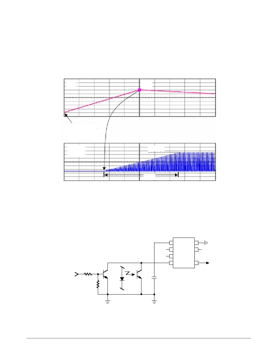
Figure 19. The burst frequency becomes so low that it is difficult to keep
an adequate level on the auxiliary V
CC
. . .
u
30 ms
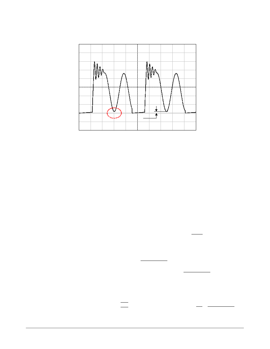
Lowering the Standby Power with Skip-Cycle
Skip-cycle offers an efficient way to reduce the standby
power by skipping unwanted cycles at light loads.
However, the recurrent frequency in skip often enters the
audible range and a high peak current obviously generates
acoustic noise in the transformer. The noise takes its origins
in the resonance of the transformer mechanical structure
which is excited by the skipping pulses. A possible
solution, successfully implemented in the NCP1200 series,
also authorizes skip-cycle but only when the power
demand has dropped below a given level. At this time, the
peak current is reduced and no noise can be heard.
Figure 20 pictures the peak current evolution of the
NCP101X entering standby.
NCP1010, NCP1011, NCP1012, NCP1013, NCP1014
http://onsemi.com
14
Figure 20. Low Peak Current Skip-Cycle Guarantees Noise-Free Operation
100%
Peak current
at nominal power
25%
Skip-cycle
current limit
Full power operation involves the nominal switching
frequency and thus avoids any noise when running.
Experiments carried on a 5.0 W universal mains board
unveiled a standby power of 300 mW @ 230 Vac with the
DSS activated and dropped to less than 100 mW when an
auxiliary winding is connected.
Frequency Jittering for Improved EMI Signature
By sweeping the switching frequency around its nominal
value, it spreads the energy content on adjacent frequencies
rather than keeping it centered in one single ray. This offers
the benefit to artificially reduce the measurement noise on
a standard EMI receiver and pass the tests more easily. The
EMI sweep is implemented by routing the V
CC
ripple
(induced by the DSS activity) to the internal oscillator. As a
result, the switching frequency moves up and down to the
DSS rhythm. Typical deviation is
"3.3% of the nominal
frequency. With a 1.0 V peak-to-peak ripple, the frequency
will equal 65 kHz in the middle of the ripple and will
increase as V
CC
rises or decrease as V
CC
ramps down.
Figure 21 portrays the behavior we have adopted.
Figure 21. The V
CC
ripple is used to introduce a frequency jittering on the internal oscillator sawtooth.
Here, a 65 kHz version was selected.
V
CC
Ripple
VCC
OFF
67.15 kHz
65 kHz
62.85 kHz
VCC
ON
Internal Sawtooth
NCP1010, NCP1011, NCP1012, NCP1013, NCP1014
http://onsemi.com
15
Soft-Start
The NCP101X features an internal 1.0 ms soft-start
activated during the power on sequence (PON). As soon as
V
CC
reaches VCC
OFF
, the peak current is gradually
increased from nearly zero up to the maximum internal
clamping level (e.g. 350 mA). This situation lasts 1.0 ms
and further to that time period, the peak current limit is
blocked to the maximum until the supply enters regulation.
The soft-start is also activated during the over current burst
(OCP) sequence. Every restart attempt is followed by a
soft-start activation. Generally speaking, the soft-start will
be activated when V
CC
ramps up either from zero (fresh
power-on sequence) or 4.7 V, the latch-off voltage
occurring during OCP. Figure 22 portrays the soft-start
behavior. The time scales are purposely shifted to offer a
better zoom portion.
Figure 22. Soft-Start is activated during a startup sequence or an OCP condition.
0 V (Fresh PON)
or
4.7 V (Overload)
V
CC
8.5 V
Current
Sense
Max Ip
1.0 ms
Non-Latching Shutdown
In some cases, it might be desirable to shut off the part
temporarily and authorize its restart once the default has
disappeared. This option can easily be accomplished
through a single NPN bipolar transistor wired between FB
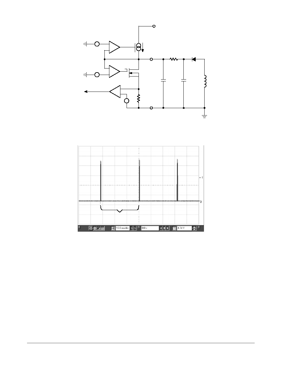
and ground. By pulling FB below the internal skip level
(Vskip), the output pulses are disabled. As soon as FB is
relaxed, the IC resumes its operation. Figure 23 depicts the
application example.
Figure 23. A non-latching shutdown where pulses are stopped as long as the NPN is biased.
ON/OFF
2
7
3
4
5
1
8
Drain
+
CV
cc
NCP1010, NCP1011, NCP1012, NCP1013, NCP1014
http://onsemi.com
16
Full Latching Shutdown
Other applications require a full latching shutdown, e.g.
when an abnormal situation is detected (overtemperature
or overvoltage). This feature can easily be implemented
through two external transistors wired as a discrete SCR.
When the OVP level exceeds the Zener breakdown
voltage, the NPN biases the PNP and fires the equivalent
SCR, permanently bringing down the FB pin. The
switching pulses are disabled until the user unplugs the
power supply.
Figure 24. Two Bipolars Ensure a Total Latch-Off of the SMPS in Presence of an OVP
2
7
3
4
5
1
8
Drain
+
CV
cc
BAT54
10 k
10 k
OVP
Rhold
12 k
Rhold ensures that the SCR stays on when fired. The bias
current flowing through Rhold should be small enough to let
the V
CC
ramp up (8.5 V) and down (7.5 V) when the SCR
is fired. The NPN base can also receive a signal from a
temperature sensor. Typical bipolars can be MMBT2222
and MMBT2907 for the discrete latch. The MMBT3946
features two bipolars NPN+PNP in the same package and
could also be used.
Power Dissipation and Heatsinking
The NCP101X welcomes two dissipating terms, the DSS
current-source (when active) and the MOSFET. Thus,
Ptot = P
DSS
+ P
MOSFET
. When the PDIP-7 package is
surrounded by copper, it becomes possible to drop its
thermal resistance junction-to-ambient, R
qJA
down
to 75
∞
C/W and thus dissipate more power. The
maximum power the device can thus evacuate is:
Pmax
+
TJmax
*
Tambmax
R
q
JA
(eq. 12)
which gives around
1.0 W for an ambient of 50
∞
C. The losses inherent to the
MOSFET R
DSon
can be evaluated using the following
formula:
Pmos
+
1
3
∑ Ip2 ∑ d ∑ RDSon
(eq. 13)
, where Ip
is the worse case peak current (at the lowest line input), d is
the converter operating duty-cycle and R
DSon
, the
MOSFET resistance for T
J
= 100
∞
C. This formula is only
valid for Discontinuous Conduction Mode (DCM)
operation where the turn-on losses are null (the primary
current is zero when you restart the MOSFET). Figure 25
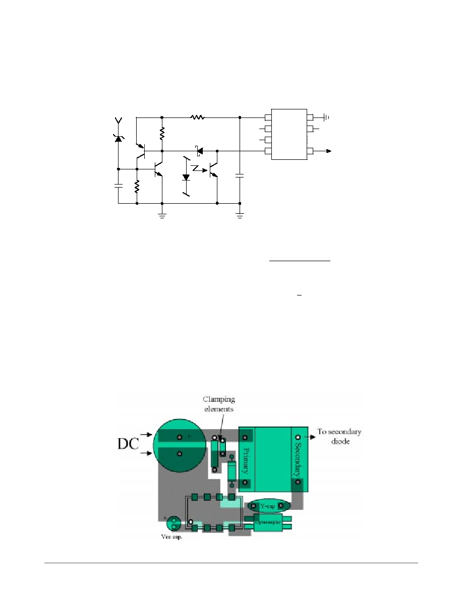
gives a possible layout to help drop the thermal resistance.
When measured on a 35
mm (1 oz) copper thickness PCB,
we obtained a thermal resistance of 75
∞
C/W.
Figure 25. A Possible PCB Arrangement to Reduce the Thermal Resistance Junction-to-Ambient
NCP1010, NCP1011, NCP1012, NCP1013, NCP1014
http://onsemi.com
17
Design Procedure
The design of an SMPS around a monolithic device does
not differ from that of a standard circuit using a controller
and a MOSFET. However, one needs to be aware of certain
characteristics specific of monolithic devices:
Figure 26. The Drain-Source Wave Shall Always be Positive . . .
1.004M
1.011M
1.018M
1.025M
1.032M
-50.0
50.0
150
250
350
> 0 !!
1. In any case, the lateral MOSFET body-diode shall
never be forward biased, either during startup
(because of a large leakage inductance) or in
normal operation as shown by Figure 26.
As a result, the Flyback voltage which is reflected on the
drain at the switch opening cannot be larger than the input
voltage. When selecting components, you thus must adopt
a turn ratio which adheres to the following equation:
N ∑ (Vout
)
Vf)
t
Vin min
(eq. 14)
. For instance, if
operating from a 120 V DC rail, with a delivery of 12 V, we
can select a reflected voltage of 100 Vdc maximum:
120≠100 > 0. Therefore, the turn ratio Np:Ns must be
smaller than 100/(12 + 1) = 7.7 or Np:Ns < 7.7. We will see
later on how it affects the calculation.
2. A current-mode architecture is, by definition,
sensitive to subharmonic oscillations.
Subharmonic oscillations only occur when the
SMPS is operating in Continuous Conduction
Mode (CCM) together with a duty-cycle greater
than 50%. As a result, we recommend to operate
the device in DCM only, whatever duty-cycle it
implies (max = 65%). However, CCM operation
with duty-cycles below 40% is possible.
3. Lateral MOSFETs have a poorly dopped
body-diode which naturally limits their ability to
sustain the avalanche. A traditional RCD clamping
network shall thus be installed to protect the
MOSFET. In some low power applications,
a simple capacitor can also be used since
Vdrain max
+
Vin
)
N ∑ (Vout
)
Vf)
)
Ip ∑
Lf
Ctot
(eq. 15)
, where Lf is the leakage inductance,
Ctot is the total capacitance at the drain node
(which is increased by the capacitor wired between
drain and source), N the Np:Ns turn ratio, Vout the
output voltage, Vf the secondary diode forward
drop and finally, Ip the maximum peak current.
Worse case occurs when the SMPS is very close to
regulation, e.g. the Vout target is almost reached
and Ip is still pushed to the maximum.
Taking into account all previous remarks, it becomes
possible to calculate the maximum power that can be
transferred at low line.
When the switch closes, Vin is applied across the primary
inductance Lp until the current reaches the level imposed by
the feedback loop. The duration of this event is called the ON
time and can be defined by:
ton
+
Lp ∑ Ip
Vin
(eq. 16)
At the switch opening, the primary energy is transferred
to the secondary and the flyback voltage appears across
Lp, resetting the transformer core with a slope of
N ∑ (Vout
)
Vf)
Lp
. toff, the OFF time is thus:
toff
+
Lp ∑ Ip
N ∑ (Vout
)
Vf)
(eq. 17)
If one wants to keep DCM only, but still need to pass the
maximum power, we will not allow a dead-time after the
core is reset, but rather immediately restart. The switching
time can be expressed by:
Tsw
+
toff
)
ton
+
Lp ∑ Ip ∑
1
Vin
)
1
N ∑ (Vout
)
Vf)
(eq. 18)

NCP1010, NCP1011, NCP1012, NCP1013, NCP1014
http://onsemi.com
18
The Flyback transfer formula dictates that:
Pout
h +
1
2
∑ Lp ∑ Ip2 ∑ Fsw
(eq. 19)
which, by extracting
Ip and plugging into Equation 19, leads to:
Tsw
+
Lp
2 ∑ Pout
h
∑ Fsw ∑ Lp
∑
1
Vin
)
1
N ∑ (Vout
)
Vf)
(eq. 20)
Extracting Lp from Equation 20 gives:
Lpcritical
+
(Vin ∑ Vr)2 ∑
h
2 ∑ Fsw ∑ [Pout ∑ (Vr2
)
2 ∑ Vr ∑ Vin
)
Vin2)]
(eq. 21)
, with Vr = N . (Vout + Vf) and
h the efficiency.
If Lp critical gives the inductance value above which
DCM operation is lost, there is another expression we can
write to connect Lp, the primary peak current bounded by
the NCP101X and the maximum duty-cycle that needs to
stay below 50%:
Lpmax
+
DCmax ∑ Vinmin ∑ Tsw
Ipmax
(eq. 22)
where Vinmin
corresponds to the lowest rectified bulk voltage, hence the
longest ton duration or largest duty-cycle. Ip max is the
available peak current from the considered part, e.g. 350 mA
typical for the NCP1013 (however, the minimum value of
this parameter shall be considered for reliable evaluation).
Combining Equations 21 and 22 gives the maximum
theoretical power you can pass respecting the peak current
capability of the NCP101X, the maximum duty-cycle and
the discontinuous mode operation:
Pmax :
+
Tsw2 ∑ Vinmin2 ∑ Vr2 ∑
h
∑
(eq. 23)
Fsw
(2 ∑ Lpmax ∑ Vr2
)
4 ∑ Lpmax ∑ Vr ∑ Vinmin
)
2 ∑ Lpmax ∑ Vinmin2)
From Equation 22 we obtain the operating duty-cycle
d
+
Ip ∑ Lp
Vin ∑ Tsw
(eq. 24)
which lets us calculate the RMS
current circulating in the MOSFET:
IdRMS
+
Ip ∑
d
3
(eq. 25)
. From this equation, we
obtain the average dissipation in the MOSFET:
Pavg
+
1
3
∑ Ip2 ∑ d ∑ RDSon
(eq. 26)
to which switching
losses shall be added.
If we stick to Equation 23, compute Lp and follow the
above calculations, we will discover that a power supply
built with the NCP101X and operating from a 100 Vac line
minimum will not be able to deliver more than 7.0 W
continuous, regardless of the selected switching frequency
(however the transformer core size will go down as
Fswitching is increased). This number increases
significantly when operated from a single European mains
(18 W). Application note AND8125/D, "Evaluating the
Power Capability of the NCP101X Members" details how
to assess the available power budget from all the NCP101X
series.
Example 1. A 12 V 7.0 W SMPS operating on a large
mains with NCP101X:
Vin = 100 Vac to 250 Vac or 140 Vdc to 350 Vdc once
rectified, assuming a low bulk ripple
Efficiency = 80%
Vout = 12 V, Iout = 580 mA
Fswitching = 65 kHz
Ip max = 350 mA ≠ 10% = 315 mA
Applying the above equations leads to:
Selected maximum reflected voltage = 120 V
with Vout = 12 V, secondary drop = 0.5 V
Np:Ns = 1:0.1
Lp critical = 3.2 mH
Ip = 292 mA
Duty-cycle worse case = 50%
Idrain RMS = 119 mA
P
MOSFET
= 354 mW at R
DSon
= 24
W (T
J
> 100
∞
C)
P
DSS
= 1.1 mA x 350 V = 385 mW, if DSS is used
Secondary diode voltage stress = (350 x 0.1) + 12 = 47 V
(e.g. a MBRS360T3, 3.0 A/60 V would fit)
Example 2. A 12 V 16 W SMPS operating on narrow
European mains with NCP101X:
Vin = 230 Vac
" 15%, 276 Vdc for Vin min to 370 Vdc
once rectified
Efficiency = 80%
Vout = 12 V, Iout = 1.25 A
Fswitching = 65 kHz
Ip max = 350 mA ≠ 10% = 315 mA
Applying the equations leads to:
Selected maximum reflected voltage = 250 V
with Vout = 12 V, secondary drop = 0.5 V
Np:Ns = 1:0.05
Lp = 6.6 mH
Ip = 0.305 mA
Duty-cycle worse case = 0.47
Idrain RMS = 121 mA
P
MOSFET
= 368 mW at R
DSon
= 24
W (T
J
> 100
∞
C)
P
DSS
= 1.1 mA x 370 V = 407 mW, if DSS is used below an
ambient of 50
∞
C.
Secondary diode voltage stress = (370 x 0.05) + 12 = 30.5 V
(e.g. a MBRS340T3, 3.0 A/40 V)
Please note that these calculations assume a flat DC rail
whereas a 10 ms ripple naturally affects the final voltage
available on the transformer end. Once the Bulk capacitor has
been selected, one should check that the resulting ripple (min
Vbulk?) is still compatible with the above calculations. As an
example, to benefit from the largest operating range, a 7.0 W
board was built with a 47
mF bulk capacitor which ensured
discontinuous operation even in the ripple minimum waves.

NCP1010, NCP1011, NCP1012, NCP1013, NCP1014
http://onsemi.com
19
MOSFET Protection
As in any Flyback design, it is important to limit the
drain excursion to a safe value, e.g. below the MOSFET
BV
DSS
which is 700 V. Figure 27 presents possible
implementations:
Figure 27. Different Options to Clamp the Leakage Spike
+
NCP101X
CVcc
HV
1
8
2
3
4
7
5
+
CVcc
HV
Rclamp
Cclamp
D
1
8
2
3
4
7
5
+
CVcc
HV
D
1
8
2
3
4
7
5
+
C
Dz
A
B
C
NCP101X
NCP101X
Figure 27A: The simple capacitor limits the voltage
according to Equation 15. This option is only valid for low
power applications, e.g. below 5.0 W, otherwise chances
exist to destroy the MOSFET. After evaluating the leakage
inductance, you can compute C with Equation 15. Typical
values are between 100 pF and up to 470 pF. Large
capacitors increase capacitive losses.
Figure 27B: This diagram illustrates the most standard
circuitry called the RCD network. Rclamp and Cclamp are
calculated using the following formulas:
Rclamp
+
2 ∑ Vclamp ∑ (Vclamp
*
(Vout
)
Vf sec) ∑ N)
Lleak ∑ Ip2 ∑ Fsw
(eq. 27)
Cclamp
+
Vclamp
Vripple ∑ Fsw ∑ Rclamp
(eq. 28)
Vclamp is usually selected 50-80 V above the reflected
value N x (Vout + Vf). The diode needs to be a fast one and
a MUR160 represents a good choice. One major drawback
of the RCD network lies in its dependency upon the peak
current. Worse case occurs when Ip and Vin are maximum
and Vout is close to reach the steady-state value.
Figure 27C: This option is probably the most expensive of
all three but it offers the best protection degree. If you need
a very precise clamping level, you must implement a Zener
diode or a TVS. There are little technology differences
behind a standard Zener diode and a TVS. However, the die
area is far bigger for a transient suppressor than that of Zener.
A 5.0 W Zener diode like the 1N5388B will accept 180 W
peak power if it lasts less than 8.3 ms. If the peak current in
the worse case (e.g. when the PWM circuit maximum
current limit works) multiplied by the nominal Zener
voltage exceeds these 180 W, then the diode will be
destroyed when the supply experiences overloads. A
transient suppressor like the P6KE200 still dissipates 5.0 W
of continuous power but is able to accept surges up to 600 W
@ 1.0 ms. Select the Zener or TVS clamping level between
40 to 80 V above the reflected output voltage when the
supply is heavily loaded.
NCP1010, NCP1011, NCP1012, NCP1013, NCP1014
http://onsemi.com
20
Typical Application Examples
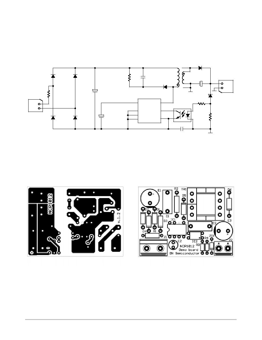
A 6.5 W NCP1012-Based Flyback Converter
Figure 28 shows a converter built with a NCP1012
delivering 6.5 W from a universal input. The board uses the
Dynamic Self-Supply and a simplified Zener-type
feedback. This configuration was selected for cost reasons
and a more precise circuitry can be used, e.g. based on a
TL431:
Figure 28. An NCP1012-Based Flyback Converter Delivering 6.5 W
1
2
J1
CEE7.5/2
D1
D2
E1
10
m
/400 V
E2
10
m
/16 V
2
3
7
2
1
GND
GND
GND
V
CC
HV
FB
GND
IC1
NCP1012
R2
150 k
D5
U160
5
4
4
8
C2
2n2/Y
4
8
7
6
5
TR1
1
E3
470
m
/25 V
D6
B150
R3
100 R
R4
180 R
2
1
ZD1
11 V
J2
CZM5/2
IC2
PC817
C1
2.2 nF
1N4007
1N4007
R1
47 R
D3
D4
1N4007
1N4007
The converter built according to Figure 29 layouts, gave
the following results:
∑
Efficiency at Vin = 100 Vac and Pout = 6.5 W = 75.7%
∑
Efficiency at Vin = 230 Vac and Pout = 6.5 W = 76.5%
Figure 29. The NCP1012-Based PCB Layout . . . and its Associated Component Placement

NCP1010, NCP1011, NCP1012, NCP1013, NCP1014
http://onsemi.com
21
A 7.0 W NCP1013-based Flyback Converter
Featuring Low Standby Power
Figure 30 depicts another typical application showing a
NCP1013-65 kHz operating in a 7.0 W converter up to
70
∞
C of ambient temperature. We can increase the output
power since an auxiliary winding is used, the DSS is
disabled, and thus offering more room for the MOSFET. In
this application, the feedback is made via a TLV431 whose
low bias current (100
mA min) helps to lower the no-load
standby power.
Figure 30. A Typical Converter Delivering 7.0 W from a Universal Mains
1
8
2
3
4
7
5
V
CC
NC
NC
FB
GND
NC
D
Vbulk
C2
47
m
F/
450 V
+
1N4148
D4
R2
3.3 k
+ C10
33
m
F/25 V
R4 22
NCP1013P06
+ 100
m
F/10 V
C3
C9
1 nF
C8
10 nF
400 V
R7
100 k/
1 W
D3
MUR160
T1
12 V @
0.6 A
GND
D2
MBRS360T3
+
+
100
m
F/16 V
C7
+
C6 C8
470
m
F/16 V
R5
39 k
R3
1 k
IC1
SFH6156-2
C4
100 nF
IC2
TLV431
R6
4.3 k
C5
2.2 nF
Y1 Type
T1
Aux
L2
22
m
H
Measurements have been taken from a demonstration
board implementing the diagram in Figure 30 and the
following results were achieved, with either the auxiliary
winding in place or through the Dynamic Self-Supply:
Vin = 230 Vac, auxiliary winding, Pout = 0, Pin = 60 mW
Vin = 100 Vac, auxiliary winding, Pout = 0, Pin = 42 mW
Vin = 230 Vac, Dynamic Self-Supply, Pout = 0,
Pin = 300 mW
Vin = 100 Vac, Dynamic Self-Supply, Pout = 0,
Pin = 130 mW
Pout = 7.0 W,
h = 81% @ 230 Vac, with auxiliary winding
Pout = 7.0 W,
h = 81.3 @ 100 Vac, with auxiliary winding
For a quick evaluation of Figure 30 application example,
the following transformers are available from Coilcraft:
A9619-C, Lp = 3.0 mH, Np:Ns = 1:0.1, 7.0 W
application on universal mains, including auxiliary winding,
NCP1013-65kHz.
A0032-A, Lp = 6.0 mH, Np:Ns = 1:0.055, 10 W
application on European mains, DSS operation only,
NCP1013-65 kHz.
Coilcraft
1102 Silver Lake Road
CARY IL 60013
Email: info@coilcraft.com
Tel.: 847-639-6400
Fax.: 847-639-1469

NCP1010, NCP1011, NCP1012, NCP1013, NCP1014
http://onsemi.com
22
ORDERING INFORMATION
Device Order Number
Frequency
(kHz)
Package Type
Shipping
R
DSon
(
W
)
Ipk (mA)
NCP1010AP065
65
50 Units / Rail
23
100
NCP1010AP100
100
PDIP-7
50 Units / Rail
23
100
NCP1010AP130
130
50 Units / Rail
23
100
NCP1011APL065R2
65
PDIP-7 (Gull Wing)
1000 / Tape & Reel
23
250
NCP1010ST65T3
65
NCP1010ST100T3
100
SOT-223
4000 / Tape & Reel
23
100
NCP1010ST130T3
130
NCP1011AP065
65
NCP1011AP100
100
PDIP-7
50 Units / Rail
23
250
NCP1011AP130
130
NCP1011AP130G
130
PDIP-7
(Pb-Free)
50 Units / Rail
23
250
NCP1011APL130R2
130
PDIP-7 (Gull Wing)
1000 / Tape & Reel
23
250
NCP1011ST65T3
65
NCP1011ST100T3
100
SOT-223
4000 / Tape & Reel
23
250
NCP1011ST130T3
130
NCP1012AP065
65
NCP1012AP100
100
PDIP-7
50 Units / Rail
11
250
NCP1012AP133
130
NCP1012APL130R2
130
PDIP-7 (Gull Wing)
1000 / Tape & Reel
11
250
NCP1012ST65T3
65
NCP1012ST100T3
100
SOT-223
4000 / Tape & Reel
11
250
NCP1012ST130T3
130
NCP1013AP065
65
NCP1013AP100
100
PDIP-7
50 Units / Rail
11
350
NCP1013AP133
130
NCP1013ST65T3
65
NCP1013ST100T3
100
SOT-223
4000 / Tape & Reel
11
350
NCP1013ST130T3
130
NCP1014AP065
65
PDIP-7
50 Units / Rail
11
450
NCP1014AP065G
65
PDIP-7
(Pb-Free)
50 Units / Rail
11
450
NCP1014AP100
100
PDIP-7
50 Units / Rail
11
450
NCP1014AP100G
100
PDIP-7
(Pb-Free)
50 Units / Rail
11
450
NCP1014APL100R2
100
PDIP-7 (Gull Wing)
1000 / Tape & Reel
11
350
NCP1014ST65T3
65
SOT 223
4000 / Tape & Reel
11
450
NCP1014ST100T3
100
SOT-223
4000 / Tape & Reel
11
450
For information on tape and reel specifications, including part orientation and tape sizes, please refer to our Tape and Reel Packaging
Specifications Brochure, BRD8011/D.
Additional Gull Wing option may be available upon request. Please contact your ON Semiconductor representative.

NCP1010, NCP1011, NCP1012, NCP1013, NCP1014
http://onsemi.com
23
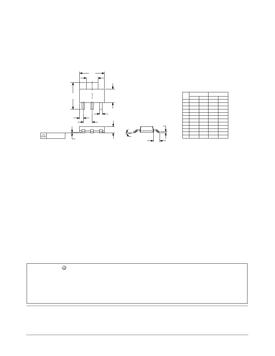
PACKAGE DIMENSIONS
PDIP-7
AP SUFFIX
CASE 626A-01
ISSUE O
NOTES:
1. DIMENSIONING AND TOLERANCING PER ANSI
Y14.5M, 1982.
2. CONTROLLING DIMENSION: MILLIMETER.
3. PACKAGE CONTOUR OPTIONAL (ROUND OR
SQUARE CORNERS).
4. DIMENSION L TO CENTER OF LEAD WHEN
FORMED PARALLEL.
5. DIMENSIONS A AND B ARE DATUMS.
1
4
5
8
F
NOTE 3
-T-
SEATING
PLANE
H
J
G
D
K
N
C
L
M
M
A
M
0.13 (0.005)
B
M
T
DIM
MIN
MAX
MIN
MAX
INCHES
MILLIMETERS
A
9.40
10.16
0.370
0.400
B
6.10
6.60
0.240
0.260
C
3.94
4.45
0.155
0.175
D
0.38
0.51
0.015
0.020
F
1.02
1.78
0.040
0.070
G
2.54 BSC
0.100 BSC
H
0.76
1.27
0.030
0.050
J
0.20
0.30
0.008
0.012
K
2.92
3.43
0.115
0.135
L
7.62 BSC
0.300 BSC
M
---
10
---
10
N
0.76
1.01
0.030
0.040
_
_
B
A
NOTES:
1. DIMENSIONS AND TOLERANCING PER
ASME Y14.5M, 1994.
2. DIMENSIONS IN INCHES.
PDIP-7, GULL WING
APL SUFFIX
CASE 626AA-01
ISSUE O
1
4
5
8
F
-H-
GAUGE
PLANE
G
K
C1
A
S
B
H
E
D
P
N
T
M
L
J
0.015
TOP VIEW
SIDE VIEW
BOTTOM VIEW
0.015 DP MAX
Bottom Ejector Pin
DIM
MIN
MAX
INCHES
A
0.365
0.385
B
0.240
0.260
C
0.120
0.150
D
0.018 TYP
E
0.039 TYP
F
0.045
0.065
G
0.100 BSC
H
0.023
0.033
J
K
0.004
0.012
L
0.036
0.044
M
0
8
N
12 TYP
P
0.300 BSC
S
0.372
0.388
_
_
_
R 0.016 TYP
0.004
FRONT VIEW
R 0.030
0.010 TYP
C1
0.124
0.162
C
NCP1010, NCP1011, NCP1012, NCP1013, NCP1014
http://onsemi.com
24
PACKAGE DIMENSIONS
SOT-223
ST SUFFIX
CASE 318E-04
ISSUE K
H
S
F
A
B
D
G
L
4
1
2
3
0.08 (0003)
C
M
K
J
DIM
A
MIN
MAX
MIN
MAX
MILLIMETERS
0.249
0.263
6.30
6.70
INCHES
B
0.130
0.145
3.30
3.70
C
0.060
0.068
1.50
1.75
D
0.024
0.035
0.60
0.89
F
0.115
0.126
2.90
3.20
G
0.087
0.094
2.20
2.40
H 0.0008 0.0040
0.020
0.100
J
0.009
0.014
0.24
0.35
K
0.060
0.078
1.50
2.00
L
0.033
0.041
0.85
1.05
M
0
10
0
10
S
0.264
0.287
6.70
7.30
NOTES:
1. DIMENSIONING AND TOLERANCING PER ANSI
Y14.5M, 1982.
2. CONTROLLING DIMENSION: INCH.
_
_
_
_
ON Semiconductor and are registered trademarks of Semiconductor Components Industries, LLC (SCILLC). SCILLC reserves the right to make changes without further notice
to any products herein. SCILLC makes no warranty, representation or guarantee regarding the suitability of its products for any particular purpose, nor does SCILLC assume any liability
arising out of the application or use of any product or circuit, and specifically disclaims any and all liability, including without limitation special, consequential or incidental damages.
"Typical" parameters which may be provided in SCILLC data sheets and/or specifications can and do vary in different applications and actual performance may vary over time. All
operating parameters, including "Typicals" must be validated for each customer application by customer's technical experts. SCILLC does not convey any license under its patent rights
nor the rights of others. SCILLC products are not designed, intended, or authorized for use as components in systems intended for surgical implant into the body, or other applications
intended to support or sustain life, or for any other application in which the failure of the SCILLC product could create a situation where personal injury or death may occur. Should
Buyer purchase or use SCILLC products for any such unintended or unauthorized application, Buyer shall indemnify and hold SCILLC and its officers, employees, subsidiaries, affiliates,
and distributors harmless against all claims, costs, damages, and expenses, and reasonable attorney fees arising out of, directly or indirectly, any claim of personal injury or death
associated with such unintended or unauthorized use, even if such claim alleges that SCILLC was negligent regarding the design or manufacture of the part. SCILLC is an Equal
Opportunity/Affirmative Action Employer. This literature is subject to all applicable copyright laws and is not for resale in any manner.
PUBLICATION ORDERING INFORMATION
N. American Technical Support: 800-282-9855 Toll Free
USA/Canada
Japan: ON Semiconductor, Japan Customer Focus Center
2-9-1 Kamimeguro, Meguro-ku, Tokyo, Japan 153-0051
Phone: 81-3-5773-3850
NCP1010/D
The products described herein (NCP1010, 1011, 1012, 1013, 1014), may be covered by one or more of the following U.S. patents: 6,271,735, 6,362,067,
6,385,060, 6,429,709, 6,587,357, 6,633,193. There may be other patents pending.
LITERATURE FULFILLMENT:
Literature Distribution Center for ON Semiconductor
P.O. Box 61312, Phoenix, Arizona 85082-1312 USA
Phone: 480-829-7710 or 800-344-3860 Toll Free USA/Canada
Fax: 480-829-7709 or 800-344-3867 Toll Free USA/Canada
Email: orderlit@onsemi.com
ON Semiconductor Website: http://onsemi.com
Order Literature: http://www.onsemi.com/litorder
For additional information, please contact your
local Sales Representative.