©
Semiconductor Components Industries, LLC, 2003
July, 2003 - Rev. 7
1
Publication Order Number:
NCP1050/D
NCP1050, NCP1051,
NCP1052, NCP1053,
NCP1054, NCP1055
Monolithic High Voltage
Gated Oscillator Power
Switching Regulator
The NCP1050 through NCP1055 are monolithic high voltage
regulators that enable end product equipment to be compliant with low
standby power requirements. This device series combines the required
converter functions allowing a simple and economical power system
solution for office automation, consumer, and industrial products.
These devices are designed to operate directly from a rectified AC line
source. In flyback converter applications they are capable of providing
an output power that ranges from 6.0 W to 40 W with a fixed AC input
of 100 V, 115 V, or 230 V, and 3.0 W to 20 W with a variable AC input
that ranges from 85 V to 265 V.
This device series features an active startup regulator circuit that
eliminates the need for an auxiliary bias winding on the converter
transformer, fault detector and a programmable timer for converter
overload protection, unique gated oscillator configuration for extremely
fast loop response with double pulse suppression, power switch current
limiting, input undervoltage lockout with hysteresis, thermal shutdown,
and auto restart fault detection. These devices are available in
economical 8-pin dual-in-line and 4-pin SOT-223 packages.
Features
∑
Startup Circuit Eliminates the Need for Transformer Auxiliary Bias
Winding
∑
Optional Auxiliary Bias Winding Override for Lowest Standby
Power Applications
∑
Converter Output Overload and Open Loop Protection
∑
Auto Restart Fault Protection
∑
IC Thermal Fault Protection
∑
Unique, Dual Edge, Gated Oscillator Configuration for Extremely
Fast Loop Response
∑
Oscillator Frequency Dithering with Controlled Slew Rate Driver for
Reduced EMI
∑
Low Power Consumption Allowing European Blue Angel Compliance
∑
On-Chip 700 V Power Switch Circuit and Active Startup Circuit
∑
Rectified AC Line Source Operation from 85 V to 265 V
∑
Input Undervoltage Lockout with Hysteresis
∑
Oscillator Frequency Options of 44 kHz, 100 kHz, 136 kHz
Typical Applications
∑
AC-DC Converters
∑
Wall Adapters
∑
Portable Electronic Chargers
∑
Low Power Standby and Keep-Alive Supplies
DIP-8
CASE 626A
P SUFFIX
1
8
MARKING
DIAGRAMS
X
= Current Limit (0, 1, 2, 3, 4, 5)
Z
= Oscillator Frequency (A, B, C)
A
= Assembly Location
WL, L
= Wafer Lot
YY, Y
= Year
WW, W = Work Week
1
8
Pin: 1.
V
CC
2.
Control Input
3, 7-8. Ground
4.
No Connection
5.
Power Switch Drain
NCP105XZ
AWL
YYWW
See detailed ordering and shipping information on page 22 of
this data sheet.
ORDERING INFORMATION
http://onsemi.com
SOT-223
CASE 318E
ST SUFFIX
1
4
N5XZ
ALYW
Pin: 1. V
CC
2. Control Input
3. Power Switch Drain
4. Ground
1
4
NCP1050, NCP1051, NCP1052, NCP1053, NCP1054, NCP1055
http://onsemi.com
2
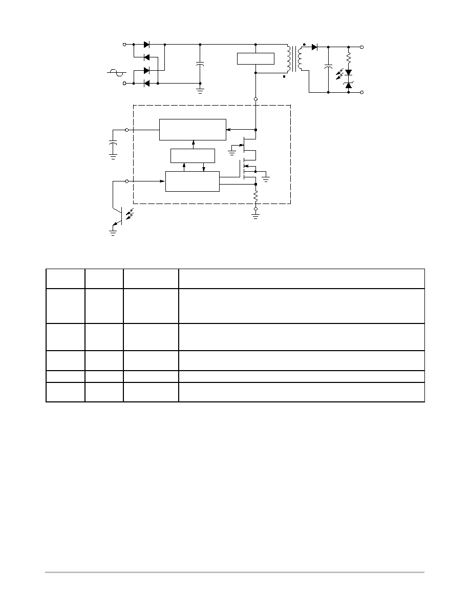
Figure 1. Typical Application
Startup & V
CC
Regulator Circuit
V
CC
Fault Detector
Power
Switch
Circuit
Oscillator &
Gating Logic
Control Input
Power Switch Circuit Output
3, 7-8
1
2
5
+
Snubber
+
+
+
-
Converter
DC Output
AC Line
Input
Ground
Pin Function Description
Pin
(SOT-223)
Pin
(DIP-8)
Function
Description
1
1
V
CC
This is the positive supply voltage input. During startup, power is supplied to this input
from Pin 5. When V
CC
reaches V
CC
(on), the Startup Circuit turns off and the output is
allowed to begin switching with 1.0 V hysteresis on the V
CC
pin. The capacitance
connected to this pin programs fault timing and frequency modulation rate.
2
2
Control Input
The Power Switch Circuit is turned off when a current greater than approximately
50
m
A is drawn out of or applied to this pin. A 10 V clamp is built onto the chip to
protect the device from ESD damage or overvoltage conditions.
4
3, 7, 8
Ground
This pin is the control circuit and Power Switch Circuit ground. It is part of the
integrated circuit lead frame.
-
4
No Connection
3
5
Power Switch
Drain
This pin is designed to directly drive the converter transformer primary, and internally
connects to Power Switch and Startup Circuit.
NCP1050, NCP1051, NCP1052, NCP1053, NCP1054, NCP1055
http://onsemi.com
3
-
+
Snubber
Startup
Circuit
Internal
Bias
Leading Edge
Blanking
Thermal
Shutdown
Oscillator
Fault
Detector
-
+
R
S
Q
Ck
R
Q
-
+
S
R
Q
+
+
+
+
+
+
+
+
+
-
Converter
DC Output
Power Switch Circuit Output
Ground
Control
Input
AC Line
Input
Driver
Power
Switch
Circuit
Turn Off
Latch
Turn On
Latch
Fault
Latch
V
CC
Bypass/
Fault Timing/
V
CO
Sweep
Control
10 V
Current Limit
Comparator
2.6 V
3.3 V
10 V
48
m
A
48
m
A
I
H
= 10
m
A
I
H
= 10
m
A
Undervoltage
Lockout
V
CC
Figure 2. Representative Block Diagram
Startup/V
CC
Reg
7.5/8.5 V
4.5 V
V
CC
R
SENSE
NCP1050, NCP1051, NCP1052, NCP1053, NCP1054, NCP1055
http://onsemi.com
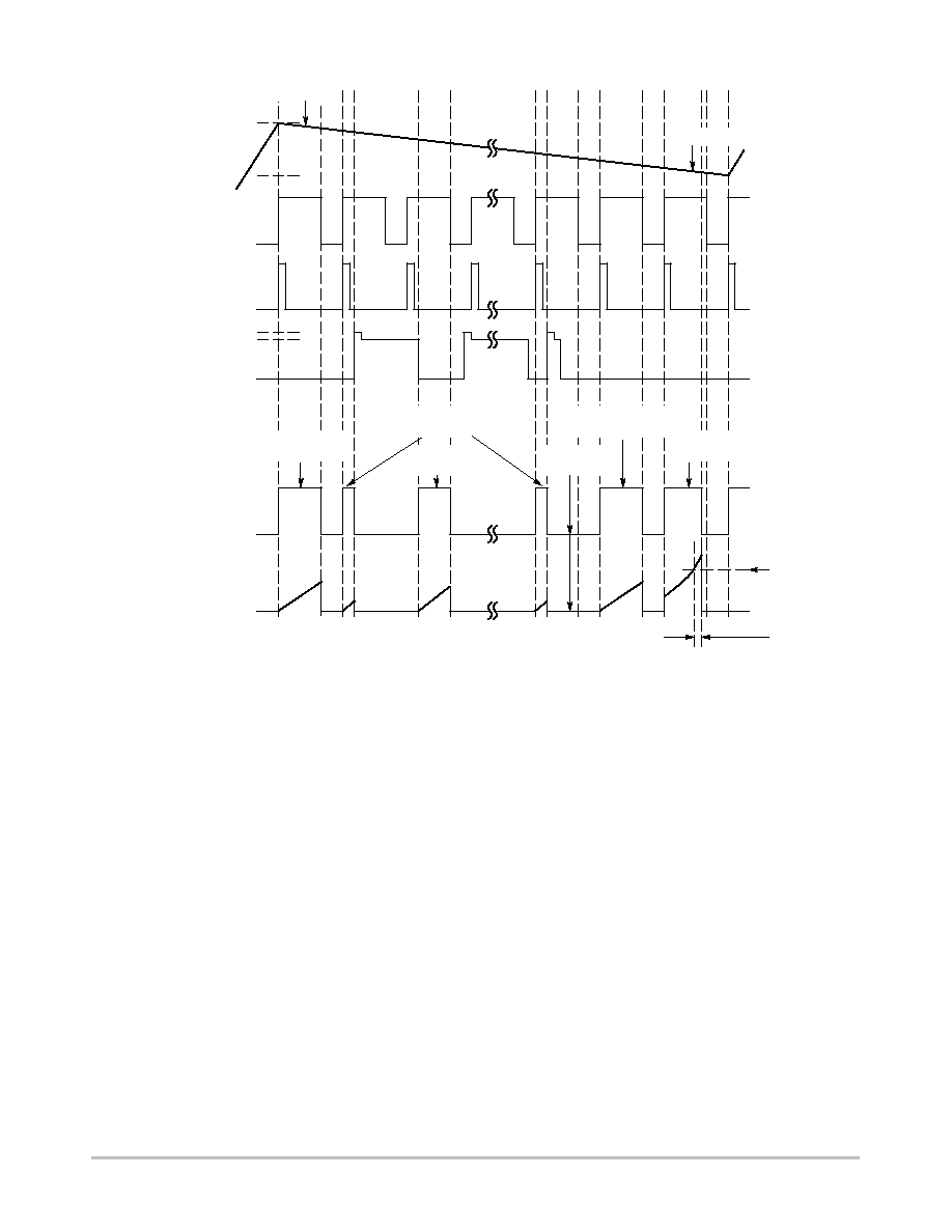
4
Leading Edge On
Feedback Off
Delay On
Duty Cycle Off
Leading Edge On
Duty Cycle Off
Leading Edge On
Current Limit Off
Leading Edge On
Duty Cycle Off
No Second
Pulse
Primary Current
Power Switch
Circuit Gate Drive
0
m
A
37.5
m
A
47.5
m
A
Oscillator Clock
Oscillator Duty
Cycle
7.5 V
8.5 V
V
CC
Current Limit
Threshold
Current Limit
Propagation
Delay
I
CONTROL, SINK
Figure 3. Timing Diagram for Gated Oscillator with Dual Edge PWM
f
OSC (high)
f
OSC (low)
NCP1050, NCP1051, NCP1052, NCP1053, NCP1054, NCP1055
http://onsemi.com
5
V
(pin 5)
0
m
A
37.5
m
A
47.5
m
A
I
CONTROL, SINK
V
CC
V
CC(reset)
V
CC(off)
V
CC(on)
0 V
I
(start)
6.3 mA
0 mA
I
CC1
I
CC2
I
CC3
0 mA
I
(start)
Fault Applied
Fault Removed
Hysteretic Regulation
I
CC1
, Current Measurement
I
CC2
, Current Measurement
I
CC3
, Current Measurement
Figure 4. Non-Latching Fault Condition Timing Diagram
I
CC

NCP1050, NCP1051, NCP1052, NCP1053, NCP1054, NCP1055
http://onsemi.com
6
MAXIMUM RATINGS
(Note 1)
Rating
Symbol
Value
Unit
Power Switch and Startup Circuit
Drain Voltage Range
Drain Current Peak During Transformer Saturation
V
DS
I
DS(pk)
*
0.3 to 700
2.0 I
lim
Max
V
A
Power Supply/V
CC
Bypass and Control Input
Voltage Range
Current
V
IR
I
max
*
0.3 to 10
100
V
mA
Thermal Characteristics
P Suffix, Plastic Package Case 626A-01
Junction-to-Lead
Junction-to-Air, 2.0 Oz. Printed Circuit Copper Clad
0.36 Sq. Inch
1.0 Sq. Inch
ST Suffix, Plastic Package Case 318E-04
Junction-to-Lead
Junction-to-Air, 2.0 Oz. Printed Circuit Copper Clad
0.36 Sq. Inch
1.0 Sq. Inch
R
q
JL
R
q
JA
R
q
JL
R
q
JA
9.0
77
60
14
74
55
∞
C/W
Operating Junction Temperature
T
J
*
40 to +150
∞
C
Storage Temperature
T
stg
*
65 to +150
∞
C
1. Maximum Ratings are those values beyond which damage to the device may occur. Exposure to these conditions or conditions beyond those
indicated may adversely affect device reliability. Functional operation under absolute maximum-rated conditions is not implied. Functional
operation should be restricted to the Recommended Operating Conditions.
A. This device series contains ESD protection and exceeds the following tests:
Pins 1-3: Human Body Model 2000 V per MIL-STD-883, Method 3015.
Machine Model Method 400 V.
Pin 5: Human Body Model 1000 V per MIL-STD-883, Method 3015.
Machine Model Method 400 V.
Pin 5 is connected to the power switch and start-up circuits, and is rated only to the max voltage of the part, or 700 V.
B. This device contains Latch-up protection and exceeds
$
100 mA per JEDEC Standard JESD78.

NCP1050, NCP1051, NCP1052, NCP1053, NCP1054, NCP1055
http://onsemi.com
7
ELECTRICAL CHARACTERISTICS
(V
CC
= 8.0 V, for typical values T
J
= 25
∞
C, for min/max values, T
J
is the operating junction
temperature range that applies (Note 2), unless otherwise noted.)
Characteristics
Symbol
Min
Typ
Max
Unit
OSCILLATOR
Frequency (V
CC
= 7.5 V)
T
J
= 25
∞
C:
A Suffix Device
B Suffix Device
C Suffix Device
T
J
= T
low
to T
high
A Suffix Device
B Suffix Device
C Suffix Device
f
OSC(low)
38
87
119
37
84
113
42.5
97
132
-
-
-
47
107
145
47
107
145
kHz
Frequency (V
CC
= 8.5 V)
T
J
= 25
∞
C:
A Suffix Device
B Suffix Device
C Suffix Device
T
J
= T
low
to T
high
A Suffix Device
B Suffix Device
C Suffix Device
f
OSC(high)
41
93
126
39
90
120
45.5
103
140
-
-
-
50
113
154
50
113
154
kHz
Frequency Sweep (V
CC
= 7.5 V to 8.5 V, T
J
= 25
∞
C)
%f
OSC
-
5.0
-
%
Maximum Duty Cycle
D
(max)
74
77
80
%
CONTROL INPUT
Lower Window Input Current Threshold
Switching Enabled, Sink Current Increasing
Switching Disabled, Sink Current Decreasing
Upper Window Input Current Threshold
Switching Enabled, Source Current Increasing
Switching Disabled, Source Current Decreasing
I
off(low)
I
on(low)
I
off(high)
I
on(high)
-58
-50
37
25
-47.5
-37.5
47.5
37.5
-37
-25
58
50
m
A
Control Window Input Voltage
Lower (I
sink
= 25
m
A)
Upper (I
source
= 25
m
A)
V
low
V
high
1.1
4.2
1.35
4.6
1.6
5.0
V
2. Tested junction temperature range for the NCP105X series:
T
low
= -40
∞
C
T
high
= +125
∞
C
NCP1050, NCP1051, NCP1052, NCP1053, NCP1054, NCP1055
http://onsemi.com
8
ELECTRICAL CHARACTERISTICS
(V
CC
= 8.0 V, for typical values T
J
= 25
∞
C, for min/max values, T
J
is the operating junction
temperature range that applies (Note 3), unless otherwise noted.)
Characteristics
Symbol
Min
Typ
Max
Unit
POWER SWITCH CIRCUIT
Power Switch Circuit On-State Resistance
NCP1050, NCP1051, NCP1052 (I
D
= 50 mA)
T
J
= 25
∞
C
T
J
= 125
∞
C
NCP1053, NCP1054, NCP1055 (I
D
= 100 mA)
T
J
= 25
∞
C
T
J
= 125
∞
C
R
DS(on)
-
-
-
-
22
42
10
23
30
55
15
28
W
Power Switch Circuit & Startup Breakdown Voltage
(I
D(off)
= 100
m
A, T
A
= 25
∞
C)
V
(BR)DS
700
-
-
V
Power Switch Circuit & Startup Circuit Off-State Leakage Current
(V
DS
= 650 V)
T
J
= 25
∞
C
(V
DS
= 650 V)
T
J
= 125
∞
C
I
DS(off)
-
-
25
15
40
80
m
A
Switching Characteristics (R
L
= 50
W
, V
DS
set for I
D
= 0.7 I
Iim
)
Turn-on Time (90% to 10%)
Turn-off Time (10% to 90%)
t
on
t
off
-
-
20
10
-
-
ns
CURRENT LIMIT AND THERMAL PROTECTION
Current Limit Threshold (T
J
= 25
∞
C) (Note 6)
NCP1050
NCP1051
NCP1052
NCP1053
NCP1054
NCP1055
I
lim
93
186
279
372
493
632
100
200
300
400
530
680
107
214
321
428
567
728
mA
Conversion Power Deviation (T
J
= 25
∞
C) (Note 7)
I
2
f
OSC
-
0
10
%A
2
Hz
Propagation Delay, Current Limit Threshold to Power Switch Circuit Output
NCP1050, NCP1051, NCP1052
NCP1053, NCP1054, NCP1055
t
PLH
-
-
135
160
-
-
ns
Thermal Protection (V
CC
= 8.6 V) (Note 3, 4, 5)
Shutdown (Junction Temperature Increasing)
Hysteresis (Junction Temperature Decreasing)
T
sd
T
H
140
-
160
75
-
-
∞
C
STARTUP CONTROL
Startup/V
CC
Regulation
Startup Threshold/V
CC
Regulation Peak (V
CC
Increasing)
Minimum Operating/V
CC
Valley Voltage After Turn-On
Hysteresis
V
CC(on)
V
CC(off)
V
H
8.0
7.0
-
8.5
7.5
1.0
9.0
8.0
-
V
Undervoltage Lockout Threshold Voltage, V
CC
Decreasing
V
CC(reset)
4.0
4.5
5.0
V
Startup Circuit Output Current (Power Switch Circuit Output = 40 V)
V
CC
= 0 V
T
J
= 25
∞
C
T
J
= -40 to 125
∞
C
V
CC
= V
CC(on)
- 0.2 V
T
J
= 25
∞
C
T
J
= -40 to 125
∞
C
I
start
5.4
4.5
4.6
3.5
6.3
-
5.6
-
7.2
8.0
6.6
7.0
mA
Minimum Start-up Drain Voltage (I
start
= 0.5 mA, V
CC
= V
CC(on)
- 0.2 V)
V
start(min)
-
13.4
20
V
Output Fault Condition Auto Restart
(V
CC
Capacitor = 10
m
F, Power Switch Circuit Output = 40 V)
Average Switching Duty Cycle
Frequency
D
rst
f
rst
-
-
6.0
3.5
-
-
%
Hz
3. Tested junction temperature range for the NCP105X series:
T
low
= -40
∞
C
T
high
= +125
∞
C
4. Maximum package power dissipation limits must be observed.
5. Guaranteed by design only.
6. Adjust di/dt to reach I
lim
in 4.0
m
sec.
7. Consult factory for additional options including test and trim for output power accuracy.

NCP1050, NCP1051, NCP1052, NCP1053, NCP1054, NCP1055
http://onsemi.com
9
ELECTRICAL CHARACTERISTICS
(V
CC
= 8.0 V, for typical values T
J
= 25
∞
C, for min/max values, T
J
is the operating junction
temperature range that applies (Note 8), unless otherwise noted.)
Characteristics
Symbol
Min
Typ
Max
Unit
TOTAL DEVICE
Power Supply Current After UVLO Turn-On (Note 9)
Power Switch Circuit Enabled
NCP1050, NCP1051, NCP1052
A Suffix Device
B Suffix Device
C Suffix Device
NCP1053, NCP1054, NCP1055
A Suffix Device
B Suffix Device
C Suffix Device
Power Switch Circuit Disabled
Non-Fault Condition
Fault Condition
I
CC1
I
CC2
I
CC3
0.35
0.40
0.40
0.40
0.45
0.50
0.35
0.10
0.45
0.50
0.525
0.50
0.575
0.65
0.45
0.175
0.55
0.60
0.65
0.60
0.70
0.80
0.55
0.25
mA
8. Tested junction temperature range for the NCP105X series:
T
low
= -40
∞
C
T
high
= +125
∞
C
9. See Non-Latching Fault Condition Timing Diagram in Figure 4.
NCP1050, NCP1051, NCP1052, NCP1053, NCP1054, NCP1055
http://onsemi.com
10
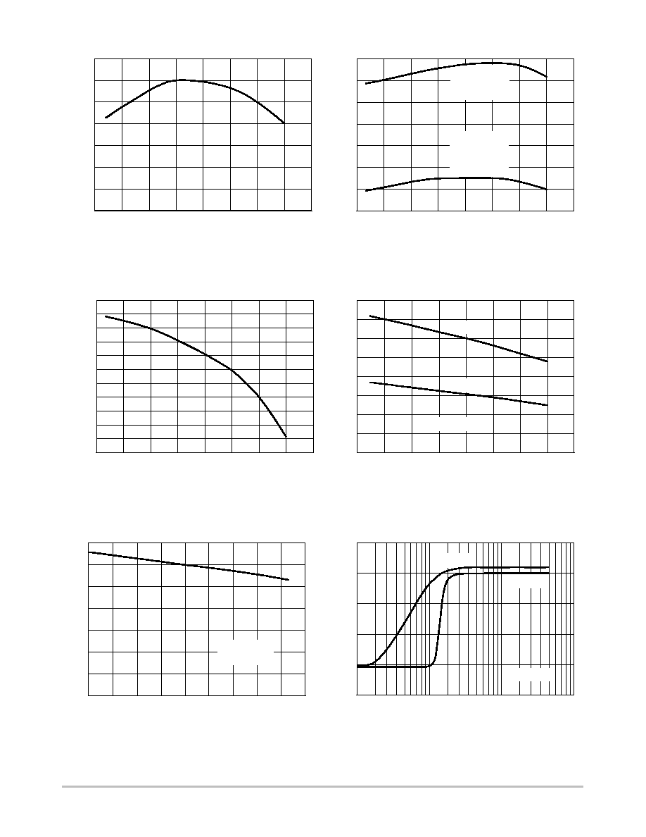
Figure 5. Oscillator Frequency (A Suffix)
versus Temperature
- 25
25
50
150
125
- 50
0
75
100
TEMPERATURE (
∞
C)
40
41
42
43
44
45
46
OSCILLA
T
OR FREQUENCY (kHz)
Figure 6. Oscillator Frequency (B Suffix)
versus Temperature
- 25
25
50
150
125
- 50
0
75
100
TEMPERATURE (
∞
C)
92
94
96
100
102
104
OSCILLA
T
OR FREQUENCY (kHz)
Figure 7. Oscillator Frequency (C Suffix)
versus Temperature
- 25
25
50
150
125
- 50
0
75
100
TEMPERATURE (
∞
C)
124
126
OSCILLA
T
OR FREQUENCY (kHz)
Figure 8. Frequency Sweep versus
Temperature
- 25
25
50
150
125
- 50
0
75
100
0
3
TEMPERATURE (
∞
C)
4
5
6
7
8
9
FREQUENCY SWEEP (kHz)
V
CC
= V
CC(on)
98
128
130
132
134
136
138
140
136 kHz
Figure 9. Maximum Duty Cycle versus
Temperature
Figure 10. Lower Window Control Input
Current Thresholds versus Temperature
100 kHz
44 kHz
142
- 25
25
50
150
125
- 50
0
75
100
76.2
76.4
TEMPERATURE (
∞
C)
76.6
76.8
77.0
77.2
77.4
77.6
MAXIMUM DUTY CYCLE (%)
- 25
25
50
150
125
- 50
0
75
100
35
TEMPERATURE (
∞
C)
40
55
SINK CONTROL CURRENT THRESHOLD (
m
A)
45
50
CURRENT RISING
CURRENT FALLING
V
CC
= V
CC(off)
V
CC
= V
CC(on)
V
CC
= V
CC(off)
V
CC
= V
CC(on)
V
CC
= V
CC(off)
2
1
30
NCP1050, NCP1051, NCP1052, NCP1053, NCP1054, NCP1055
http://onsemi.com
11
Figure 11. Upper Window Control Input
Current Thresholds versus Temperature
- 50
25
50
150
125
0
100
30
TEMPERATURE (
∞
C)
34
Figure 12. Control Input Lower Window Clamp
Voltage versus Temperature
- 25
25
50
150
125
- 50
0
75
100
1.28
1.29
TEMPERATURE (
∞
C)
1.30
1.34
1.36
1.37
1.38
1.39
CLAMP VOL
T
AGE (V)
38
42
46
50
1.35
CURRENT RISING
CURRENT FALLING
I
SINK
= 25
m
A
SOURCE CONTROL CURRENT THRESHOLD (
m
A)
Figure 13. Control Input Upper Window Clamp
Voltage versus Temperature
- 25
25
50
150
125
- 50
0
75
100
4.52
4.54
TEMPERATURE (
∞
C)
4.56
4.58
4.60
4.64
4.66
CLAMP VOL
T
AGE (V)
4.62
I
SOURCE
= 25
m
A
Figure 14. On Resistance versus Temperature
- 25
25
50
150
125
- 50
0
100
0
TEMPERATURE (
∞
C)
10
20
30
40
45
ON RESIST
ANCE (
W
)
NCP1050,1,2
(I
D
= 50 mA)
NCP1053,4,5
(I
D
= 100 mA)
Figure 15. Power Switch and Startup Circuit
Leakage Current versus Voltage
200
400
800
0
600
0
APPLIED VOLTAGE (V)
20
40
80
100
120
LEAKAGE CURRENT (
m
A)
60
Figure 16. Power Switch and Startup Circuit
Output Capacitance versus Applied Voltage
100
300
700
600
0
200
400
500
1
APPLIED VOLTAGE (V)
10
100
CAP
ACIT
ANCE (pF)
T
J
= -40
∞
C
T
J
= 25
∞
C
T
J
= 125
∞
C
T
J
= 25
∞
C
NCP1053,4,5
NCP1050,1,2
1.31
1.33
1.32
- 25
75
5
15
25
35
75
100
300
700
500
900
NCP1050, NCP1051, NCP1052, NCP1053, NCP1054, NCP1055
http://onsemi.com
12
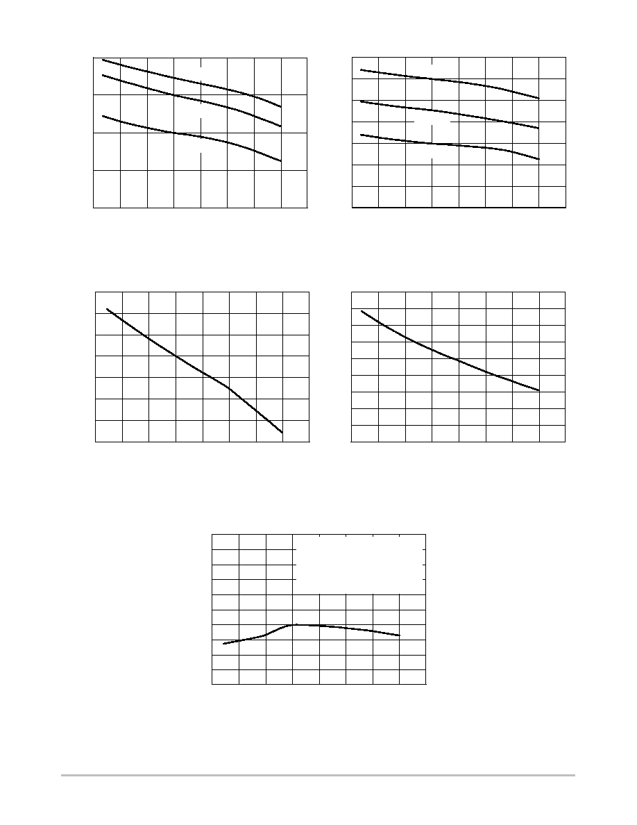
Figure 17. Normalized Peak Current Limit
versus Temperature
- 25
25
50
150
125
- 50
0
75
100
0.88
TEMPERATURE (
∞
C)
0.90
0.92
NORMALIZED CURRENT LIMIT
0.94
0.96
0.98
1.00
1.02
Figure 18. Supply Voltage Thresholds versus
Temperature
- 25
25
50
150
125
- 50
0
75
100
TEMPERATURE (
∞
C)
7.2
7.4
SUPPL
Y THRESHOLD (V)
Figure 19. Undervoltage Lockout Threshold
versus Temperature
- 25
25
50
150
125
- 50
0
75
100
4.34
4.36
TEMPERATURE (
∞
C)
4.38
4.40
4.42
4.52
4.54
4.56
UNDER
VOL
T
AGE THRESHOLD (V)
7.6
7.8
8.0
8.2
8.4
8.6
STARTUP
THRESHOLD
V
CC(on)
MINIMUM
OPERATING
THRESHOLD
V
CC(off)
4.50
Figure 20. Start Current versus Temperature
- 25
25
50
150
125
- 50
0
75
100
0
TEMPERATURE (
∞
C)
1
2
3
5
6
7
8
ST
AR
T CURRENT (mA)
4
V
CC
= 8.3 V
V
CC
= 0 V
Figure 21. Startup Current versus Supply
Voltage
1
3
4
9
7
0
2
5
6
0
SUPPLY VOLTAGE (V)
1
2
3
5
6
7
ST
AR
TUP CURRENT (mA)
4
T
J
= 25
∞
C
V
PIN 5
= 20 V
8
Figure 22. Startup Current versus Pin 5
Voltage
10
1000
1
100
-2
PIN 5 VOLTAGE (V)
0
2
6
8
ST
AR
TUP CURRENT (mA)
4
T
J
= 25
∞
C
V
CC
= 0 V
V
CC
= 8 V
4.44
4.46
4.48
V
PIN 5
= 20 V
NCP1050, NCP1051, NCP1052, NCP1053, NCP1054, NCP1055
http://onsemi.com
13
Figure 23. Supply Current versus Temperature
(NCP1050/1/2)
- 25
25
50
150
125
- 50
0
75
100
TEMPERATURE (
∞
C)
0.35
0.40
0.45
0.55
SUPPL
Y CURRENT (mA)
- 25
25
50
150
125
- 50
0
75
100
TEMPERATURE (
∞
C)
0.41
SUPPL
Y CURRENT (mA)
0.50
0.42
0.43
0.45
0.46
0.47
0.44
Figure 24. Supply Current versus Temperature
(NCP1053/4/5)
- 25
25
50
150
125
- 50
0
75
100
TEMPERATURE (
∞
C)
0.35
0.50
0.55
0.60
0.70
SUPPL
Y CURRENT (mA)
0.45
Figure 25. Supply Current When Switching
Disable versus Temperature
- 25
25
50
150
125
- 50
0
75
100
0.12
TEMPERATURE (
∞
C)
0.13
0.14
SUPPL
Y CURRENT (mA)
0.15
0.16
0.18
0.19
0.21
0.17
Figure 26. Supply Current in Fault Condition
versus Temperature
- 25
25
50
150
125
- 50
0
75
100
13.2
TEMPERATURE (
∞
C)
13.3
13.4
SUPPL
Y VOL
T
AGE (V)
13.5
13.6
13.8
13.9
14.0
13.7
Figure 27. Supply Voltage versus Temperature
13.0
13.1
136 kHz
100 kHz
44 kHz
136 kHz
100 kHz
44 kHz
0.40
CONDITION:
V
CC
pin = 1
m
F to ground
Control pin = open
Drain pin = 1 k
W
to Power Supply,
Increase Voltage Until Switching
0.65
0.48
0.20

NCP1050, NCP1051, NCP1052, NCP1053, NCP1054, NCP1055
http://onsemi.com
14
OPERATING DESCRIPTION
Introduction
The NCP105X series represents a new higher level of
integration by providing on a single monolithic chip all of
the active power, control, logic, and protection circuitry
required to implement a high voltage flyback converter and
compliance with very low standby power requirements for
modern consumer electronic power supplies. This device
series is designed for direct operation from a rectified 240
VAC line source and requires minimal external components
for a complete cost sensitive converter solution. Potential
markets include cellular phone chargers, standby power
supplies for personal computers, secondary bias supplies for
microprocessor keep-alive supplies and IR detectors. A
description of each of the functional blocks is given below,
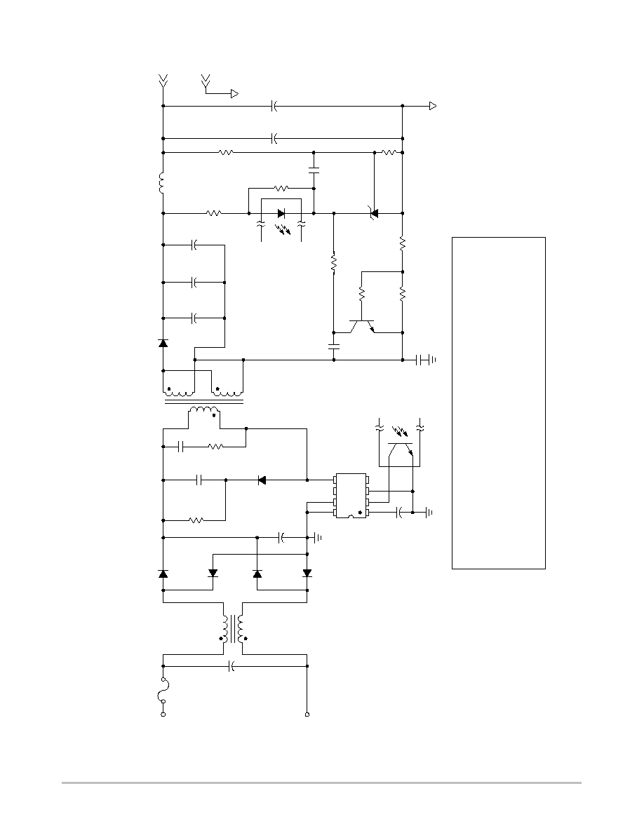
and the representative block diagram is shown in Figure 2.
This device series features an active startup regulator
circuit that eliminates the need for an auxiliary bias winding
on the converter transformer, fault logic with a programmable
timer for converter overload protection, unique gated
oscillator configuration for extremely fast loop response with
double pulse suppression, oscillator frequency dithering with
a controlled slew rate driver for reduced EMI,
cycle-by-cycle current limiting, input undervoltage lockout
with hysteresis, thermal shutdown, and auto restart or latched
off fault detect device options. These devices are available in
economical 8-pin PDIP and 4-pin SOT-223 packages.
Oscillator
The Oscillator is a unique fixed-frequency, duty-cycle-
controlled oscillator. It charges and discharges an on chip
timing capacitor to generate a precise square wave signal
used to pulse width modulate the Power Switch Circuit.
During the discharge of the timing capacitor, the Oscillator
duty cycle output holds one input of the Driver low. This
action keeps the Power Switch Circuit off, thus limiting the
maximum duty cycle.
A frequency modulation feature is incorporated into the
IC in order to aide in EMI reduction. Figure 3 illustrates this
frequency modulation feature. The power supply voltage,
V
CC
, acts as the input to the built-in voltage controlled
oscillator. As the V
CC
voltage is swept across its nominal
operating range of 7.5 to 8.5 V, the oscillator frequency is
swept across its corresponding range.
The center oscillator frequency is internally programmed
for 44 kHz, 100 kHz, or 136 kHz operation with a controlled
charge to discharge current ratio that yields a maximum
Power Switch duty cycle of 77%. The Oscillator
temperature characteristics are shown in Figures 5
through
9. Contact an ON Semiconductor sales
representative for further information regarding frequency
options.
Control Input
The Control Input pin circuit has parallel source follower
input stages with voltage clamps set at 1.35 and 4.6 V.
Current sources clamp the input current through the
followers at approximately 47.5
mA with 10 mA hysteresis.
When a source or sink current in excess of this value is
applied to this input, a logic signal generated internally
changes state to block power switch conduction. Since the
output of the Control Input sense is sampled continuously
during t
on
(77% duty cycle), it is possible to turn the Power
Switch Circuit on or off at any time within t
on
. Because it
does not have to wait for the next cycle (rising edge of the
clock signal) to switch on, and because it does not have to
wait for current limit to turn off, the circuit has a very fast
transient response as shown in Figure 3.
In a typical converter application the control input current
is drawn by an optocoupler. The collector of the optocoupler
is connected to the Control Input pin and the emitter is
connected to ground. The optocoupler LED is mounted in
series with a shunt regulator (typically a TL431) at the DC
output of the converter. When the power supply output is
greater than the reference voltage (shunt regulator voltage
plus optocoupler diode voltage drop), the optocoupler turns
on, pulling down on the Control Input. The control input
logic is configured for line input sensing as well.
Turn On Latch
The Oscillator output is typically a 77% positive duty
cycle square waveform. This waveform is inverted and
applied to the reset input of the turn-on latch to prevent any
power switch conduction during the guaranteed off time.
This square wave is also gated by the output of the control
section and applied to the set input of the same latch.
Because of this gating action, the power switch can be
activated when the control input is not asserted and the
oscillator output is high.
The use of this unique gated Turn On Latch over an
ordinary Gated Oscillator allows a faster load transient
response. The power switch is allowed to turn on
immediately, within the maximum duty cycle time period,
when the control input signals a necessary change in state.
Turn Off Latch
A Turn Off Latch feature has been incorporated into this
device series to protect the power switch circuit from
excessive current, and to reduce the possibility of output
overshoot in reaction to a sudden load removal. If the Power
Switch current reaches the specified maximum current limit,
the Current Limit Comparator resets the Turn Off Latch and
turns the Power Switch Circuit off. The turn off latch is also
reset when the Oscillator output signal goes low or the
Control Input is asserted, thus terminating output MOSFET
conduction. Because of this response to control input
signals, it provides a very fast transient response and very
tight load regulation. The turn off latch has an edge triggered
set input which ensures that the switch can only be activated
once during any oscillator period. This is commonly
referred to as double pulse suppression.

NCP1050, NCP1051, NCP1052, NCP1053, NCP1054, NCP1055
http://onsemi.com
15
Current Limit Comparator and Power Switch Circuit
The Power Switch Circuit is constructed with a
SENSEFET
TM
in order to monitor the drain current. A
portion of the current flowing through the circuit goes into
a sense element, R
sense
. The current limit comparator detects
if the voltage across R
sense
exceeds the reference level that
is present at its inverting input. If this level is exceeded, the
comparator quickly resets the Turn Off Latch, thus
protecting the Power Switch Circuit.
A Leading Edge Blanking circuit was placed in the current
sensing signal path to prevent a premature reset of the Turn
Off Latch. A potential premature reset signal is generated
each time the Power Switch Circuit is driven into conduction
and appears as a narrow voltage spike across current sense
resistor R
sense
. The spike is due to the Power Switch Circuit
gate to source capacitance, transformer interwinding
capacitance,
and output rectifier recovery time. The Leading
Edge Blanking circuit has a dynamic behavior that masks the
current signal until the Power Switch Circuit turn-on
transition is completed. The current limit propagation delay
time is typically 135 to 165 nanoseconds. This time is
measured from when an overcurrent appears at the Power
Switch Circuit drain, to the beginning of turn-off. Care must
be taken during transformer saturation so that the maximum
device current limit rating is not exceeded.
The high voltage Power Switch Circuit is monolithically
integrated with the control logic circuitry and is designed to
directly drive the converter transformer. Because the
characteristics of the power switch circuit are well known,
the gate drive has been tailored to control switching
transitions to help limit electromagnetic interference (EMI).
The Power Switch Circuit is capable of switching 700 V
with an associated drain current that ranges nominally from
0.10 to 0.68 Amps.
Startup Circuit
Rectified AC line voltage is applied to the Startup Circuit
on Pin 5, through the primary winding. The circuit is
self-biasing and acts as a constant current source, gated by
control logic. Upon application of the AC line voltage, this
circuit routes current into the supply capacitor typically
connected to Pin 1. During normal operation, this capacitor
is hysteretically regulated from 7.5 to 8.5 V by monitoring
the supply voltage with a comparator and controlling the
startup current source accordingly. This Dynamic
Self-Supply (DSS) functionality offers a great deal of
applications flexibility as well. The startup circuit is rated at
a maximum 700 V (maximum power dissipation limits must
be observed).
Undervoltage Lockout
An Undervoltage Lockout (UVLO) comparator is
included to guarantee that the integrated circuit has
sufficient voltage to be fully functional. The UVLO
comparator monitors the supply capacitor input voltage at
Pin 1 and disables the Power Switch Circuit whenever the
capacitor voltage drops below the undervoltage lockout
threshold. When this level is crossed, the controller enters a
new startup phase by turning the current source on. The
supply voltage will then have to exceed the startup threshold
in order to turn off the startup current source. Startup and
normal operation of the converter are shown in Figure 3.
Fault Detector
The NCP105X series has integrated Fault Detector
circuitry for detecting application fault conditions such as
open loop, overload or a short circuited output. A timer is
generated by driving the supply capacitor with a known
current and hysteretically regulating the supply voltage
between set thresholds. The timer period starts when the
supply voltage reaches the nominal upper threshold of 8.5 V
and stops when the drain current of the integrated circuit
draws the supply capacitor voltage down to the undervoltage
lockout threshold of 7.5 V.
If, during this timer period, no feedback has been applied
to the control input, the fault detect logic is set to indicate an
abnormal condition. This may occur, for example, when the
optocoupler fails or the output of the application is
overloaded or completely shorted. In this case, the part will
stop switching, go into a low power mode, and begin to draw
down the supply capacitor to the reset threshold voltage of
4.5 V. At that time, the startup circuit will turn on again to
drive the supply to the turn on threshold. Then the part will
begin the cycle again, effectively sampling the control input
to determine if the fault condition has been removed. This
mode is commonly referred to as burst mode operation and
is shown is Figure 4.
Proper selection of the supply capacitor allows successful
startup with monotonically increasing output voltage,
without falsely sensing a fault condition. Figure 4 shows
successful startup and the evolution of the signals involved
in the presence of a fault.
Thermal Shutdown
The internal Thermal Shutdown block protects the device
in the event that the maximum junction temperature is
exceeded. When activated, typically at 160
∞
C, one input of
the Driver is held low to disable the Power Switch Circuit.
The Power Switch is allowed to resume operation when the
junction temperature falls below 85
∞
C. The thermal
shutdown feature is provided to prevent catastrophic device
failures from accidental overheating. It is not intended to be
used as a substitute for proper heatsinking.

NCP1050, NCP1051, NCP1052, NCP1053, NCP1054, NCP1055
http://onsemi.com
16
APPLICATIONS
Two application examples have been provided in this
document, and they are described in detail in this section.
Figure 28 shows a Universal Input, 6 Watt Converter
Application as well as a 5.5 Watt Charger Application using
the NCP1053B. The Charger consists of the additional
components Q1, C13, and R7 through R10, as shown. These
were constructed and tested using the printed circuit board
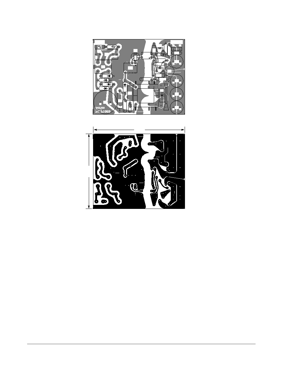
layout shown in Figure 40. The board consists of a fiberglass
epoxy material (FR4) with a single side of two ounce per
square foot (70
mm thick) copper foil. Test data from the two
applications is given in Figures 29 through 39.
Both applications generate a well-regulated output
voltage over a wide range of line input voltage and load
current values. The charger application transitions to a
constant current output if the load current is increased
beyond a preset range. This can be very effective for battery
charger application for portable products such as cellular
telephones, personal digital assistants, and pagers. Using the
NCP105X series in applications such as these offers a wide
range of flexibility for the system designer.
The NCP105X application offers a low cost alternative to
other applications. It uses a Dynamic Self-Supply (DSS)
function to generate its own operating supply voltage such
that an auxiliary transformer winding is not needed. (It also
offers the flexibility to override this function with an
auxiliary winding if ultra-low standby power is the
designer's main concern.) This product also provides for
automatic output overload, short circuit, and open loop
protection by entering a programmable duty cycle burst
mode of operation. This eliminates the need for expensive
devices overrated for power dissipation or maximum
current, or for redundant feedback loops.
The application shown in Figure 28 can be broken down
into sections for the purpose of operating description.
Components C1, L1 and C6 provide EMI filtering for the
design, although this is very dependent upon board layout,
component type, etc. D1 through D4 along with C2 provide
the AC to bulk DC rectification. The NCP1053 drives the
primary side of the transformer, and the capacitor, C5, is an
integral part of the Dynamic Self-Supply. R1, C3, and D5
comprise an RCD snubber and R2 and C4 comprise a ringing
damper both acting together to protect the IC from voltage
transients greater than 700 volts and reduce radiated noise
from the converter. Diode D6 along with C7-9, L2, C11, and
C12 rectify the transformer secondary and filter the output
to provide a tightly regulated DC output. IC3 is a shunt
regulator that samples the output voltage by virtue of R5 and
R6 to provide drive to the optocoupler, IC2, Light Emitting
Diode (LED). C10 is used to compensate the shunt regulator.
When the application is configured as a Charger, Q1 delivers
additional drive to the optocoupler LED when in constant
current operation by sampling the output current through R7
and R8.
Component Selection Guidelines
Choose snubber components R1, C3, and D5 such that the
voltage on pin 5 is limited to the range from 0 to 700 volts.
These components protect the IC from substrate injection if
the voltage was to go below zero volts, and from avalanche
if the voltage was to go above 700 volts, at the cost of slightly
reduced efficiency. For lower power design, a simple RC
snubber as shown, or connected to ground, can be sufficient.
Ensure that these component values are chosen based upon
the worst-case transformer leakage inductance and
worst-case applied voltage. Choose R2 and C4 for best
performance radiated switching noise.
Capacitor C5 serves multiple purposes. It is used along
with the internal startup circuitry to provide power to the IC
in lieu of a separate auxiliary winding. It also serves to
provide timing for the oscillator frequency sweep for
limiting the conducted EMI emissions. The value of C5 will
also determine the response during an output fault (overload
or short circuit) or open loop condition as shown in Figure 4,
along with the total output capacitance.
Resistors R5 and R6 will determine the regulated output
voltage along with the reference voltage chosen with IC3.
The base to emitter voltage drop of Q1 along with the
value of R7 will set the fixed current limit value of the
Charger application. R9 is used to limit the base current of
Q1. Component R8 can be selected to keep the current limit
fixed with very low values of output voltage or to provide
current limit foldback with results as shown in
Figures 29 and 33. A relatively large value of R8 allows for
enough output voltage to effectively drive the optocoupler
LED for fixed current limit. A low value of R8, along with
resistor R10, provides for a low average output power using
the fault protection feature when the output voltage is very
low. C13 provides for output voltage stability when the
Charger application is in current limit.
NCP1050,
NCP1051, NCP1052, NCP1053, NCP1054, NCP1055
http://onsemi.com
17
R5
2.00 k
R6
2.20 k
R4*
1.0 k
C10
0.22
IC3
TL431
2N3904
R9*
22
W
R7*
0.5
W
/1 W
IC2
SFH 615A-4
R3
47
C12
1.0
C11
220
D6
1N5822
C7
330
C8
330
C9
330
C5
10
D5
MUR160
C2
33
D2
1N4006
D1
1N4006
D3
1N4006
D4
1N4006
L1
10 mH
V
in
85 - 265 V
AC
F1
2.0 A
T1
5.25 V
1.2 A
R8*
1.2
W
/1 W
C1
0.1
NCP1053B
C6
100 p
Q1*
L2
5
m
H
Figure 28. Universal Input 6/5 W
att Converter/Charger Application
COOPER ELECTRONIC TECHNOLOGIES
PART # CTX22-15348
PRIMARY: 97 turns of #29 AWG, Pin 4 = start, Pin 5 = finish
SECONDARY: 5 turns of 0.40 mm, Pins 2 and 1 = start, Pins 7 and 8 = finish
GAP: Designed for Total 1.24 mH Primary Inductance
CORE: TSF-7070
BOBBIN: Pins 3 and 6 Removed, EE19
T1:
C4
50 p
C3
220 p
R1
91 k
R2
2.2 k
R10*
220
C13*
1.0
* Add Q1, C13, and R7-R10, and Change R4 to 2.0 k
W
for Charger Output

NCP1050, NCP1051, NCP1052, NCP1053, NCP1054, NCP1055
http://onsemi.com
18
Test
Conditions
Converter Results
Charger Results
Line Regulation
V
in
= 85 - 265 V
AC
; I
out
= 120 mA
V
in
= 85 - 265 V
AC
;
I
out
= 600 mA
V
in
= 85 - 265 V
AC
;
I
out
= 1.2 A
2 mV
1 mV
2 mV
V
in
= 85 - 265 V
AC
; I
out
= 100 mA
V
in
= 85 - 265 V
AC
;
I
out
= 500 mA
V
in
= 85 - 265 V
AC
;
I
out
= 1.00 A
11 mV
24 mV
41 mV
Load Regulation
V
in
= 85 V
AC
; I
out
= 120 mA - 1.2 A
V
in
= 110 V
AC
; I
out
= 120 mA - 1.2 A
V
in
= 230 V
AC
; I
out
= 120 mA - 1.2 A
V
in
= 265 V
AC
; I
out
= 120 mA - 1.2 A
12 mV
13 mV
12 mV
13 mV
V
in
= 85 V
AC
; I
out
= 100 mA - 1.00 A
V
in
= 110 V
AC
; I
out
= 100 mA - 1.00 A
V
in
= 230 V
AC
; I
out
= 100 mA - 1.00 A
V
in
= 265 V
AC
; I
out
= 100 mA - 1.00 A
58 mV
65 mV
71 mV
67 mV
Output Ripple
V
in
= 110 V
AC
; I
out
= 1.2 A
V
in
= 230 V
AC
; I
out
= 1.2 A
86 mV
p-p
127 mV
p-p
V
in
= 110 V
AC
; I
out
= 1.00 A
V
in
= 230 V
AC
; I
out
= 1.00 A
80 mV
p-p
155 mV
p-p
Efficiency
V
in
= 110 V
AC
; I
out
= 1.2 A
V
in
= 230 V
AC
; I
out
= 1.2 A
72.4%
69.6%
V
in
= 110 V
AC
; R
8
= 1.2
W
, I
out
= 1.00 A
V
in
= 230 V
AC
; R
8
= 1.2
W
, I
out
= 1.00 A
54.6%
53.6%
V
in
= 110 V
AC
; R
8
= 0
W
, I
out
= 1.00 A
V
in
= 230 V
AC
; R
8
= 0
W
, I
out
= 1.00 A
66.1%
63.3%
No Load Input Power
V
in
= 110 V
AC
; I
out
= 0 A
V
in
= 230 V
AC
; I
out
= 0 A
100 mW
200 mW
100 mW
200 mW
Standby Output Power
V
in
= 110 V
AC
; P
in
= 1 W
V
in
= 230 V
AC
; P
in
= 1 W
680 mW
630 mW
640 mW
540 mW
Short Circuit Load Input Power
V
in
= 110 V
AC
; V
out
= 0 V (Shorted)
V
in
= 230 V
AC
; V
out
= 0 V (Shorted)
400 mW
550 mW
V
in
= 110 V
AC
; R
8
= 1.2
W
, V
out
= 0 V (Shorted)
V
in
= 230 V
AC
; R
8
= 1.2
W
, V
out
= 0 V (Shorted)
750 mW
900 mW
V
in
= 110 V
AC
; R
8
= 0
W
, V
out
= 0 V (Shorted)
V
in
= 230 V
AC
; R
8
= 0
W
, V
out
= 0 V (Shorted)
700 mW
850 mW
Figure 29. Converter and Charger Test Data Summary
NCP1050, NCP1051, NCP1052, NCP1053, NCP1054, NCP1055
http://onsemi.com
19
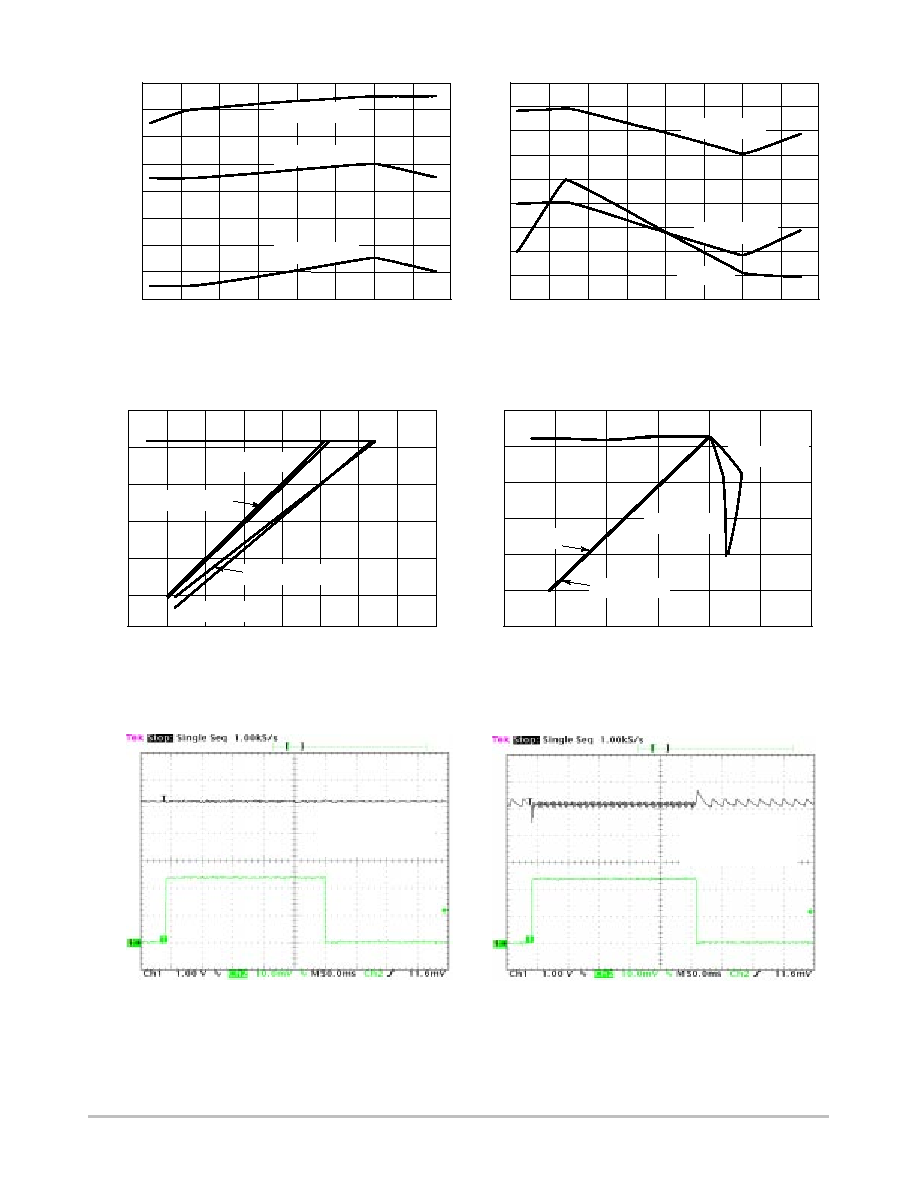
Figure 30. Converter Line Regulation
180
280
80
130
230
5.208
LINE INPUT VOLTAGE (V
AC
)
5.210
5.212
5.214
5.218
5.220
5.224
OUTPUT VOL
T
AGE (V
DC
)
Figure 31. Charger Line Regulation
Figure 32. Converter Load Regulation
1
2
0
0.5
1.5
0
LOAD CURRENT (A)
1
2
OUTPUT VOL
T
AGE (V)
Figure 33. Charger Load Regulation
3
4
5
6
Figure 34. Converter Load Transient Response
Figure 35. Charger Load Transient Response
I
out
= 120 mA
I
out
= 600 mA
I
out
= 1.2 A
V
in
= 85 V
AC
V
in
= 110 V
AC
V
in
= 230 V
AC
V
in
= 265 V
AC
180
280
80
130
230
5.14
LINE INPUT VOLTAGE (V
AC
)
5.18
5.19
5.20
5.21
5.22
5.23
OUTPUT VOL
T
AGE (V
DC
)
I
out
= 100 mA
I
out
= 500 mA
I
out
= 1 A
1.0
1.5
0
0
LOAD CURRENT (A)
1
2
OUTPUT VOL
T
AGE (V)
3
4
5
6
0.5
5.216
5.222
5.15
5.16
5.17
V
in
= 85 V
AC
V
in
= 110 V
AC
V
in
= 230 V
AC
V
in
= 265 V
AC
Ch1: V
out
Ch2: I
out
= 0.2 A/div
(V
in
= 230 V
AC
)
Ch1: V
out
Ch2: I
out
= 0.2 A/div
(V
in
= 230 V
AC
)

NCP1050, NCP1051, NCP1052, NCP1053, NCP1054, NCP1055
http://onsemi.com
20
V
in
= 85 V
AC
V
in
= 85 V
AC
V
in
= 265 V
AC
Figure 36. Converter Efficiency
1.0
0
0.5
1.5
50
LOAD CURRENT (A)
55
60
65
70
75
EFFICIENCY (%)
Figure 37. Charger Efficiency
Figure 38. Converter On/Off Line Transient
Response
Figure 39. Charger On/Off Line Transient
Response
V
in
= 110 V
AC
V
in
= 230 V
AC
V
in
= 265 V
AC
0.5
1.5
0
1.0
45
LOAD CURRENT (A)
50
55
65
EFFICIENCY (%)
V
in
= 110 V
AC
V
in
= 230 V
AC
60
70
Ch1: V
out
Ch2: Rectified V
in
(V
in
= 230 V
AC
,
I
out
= 0.5 A)
Ch1: V
out
Ch2: Rectified V
in
(V
in
= 230 V
AC
,
I
out
= 0.5 A)
NCP1050, NCP1051, NCP1052, NCP1053, NCP1054, NCP1055
http://onsemi.com
21
Board Graphics
Figure 40. Printed Circuit Board and
Component Layout
D1
D2
D4
D3
D6
DC Output
R5
IC3
L2
+
+
R3
R6
C10
+
+
C11
+
C12
IC2
C9
C8
C7
C6
T1
C2
+
IC1
+
C5
D5
R1
C3
C4
R2
L1
C1
F1
AC Input
R4
R9
R8
Q1
R7
NCP1050
Series
Top View
Bottom View
2.75
2.25
-
-
-
-
-
-
-

NCP1050, NCP1051, NCP1052, NCP1053, NCP1054, NCP1055
http://onsemi.com
22
DEVICE ORDERING INFORMATION
(Note 10)
Device
Package
Shipping
R
DS(on)
(
W
)
I
pk
(mA)
NCP1050PZZZ
100
NCP1051PZZZ
30
200
NCP1052PZZZ
DIP-8
50 Units/Rail
300
NCP1053PZZZ
DIP-8
CASE 626A
50 Units/Rail
400
NCP1054PZZZ
15
530
NCP1055PZZZ
680
NCP1050STZZZT3
100
NCP1051STZZZT3
30
200
NCP1052STZZZT3
SOT-223
4000 Units/Tape & Reel
300
NCP1053STZZZT3
SOT-223
CASE 318E
4000 Units/Tape & Reel
400
NCP1054STZZZT3
15
530
NCP1055STZZZT3
680
10. Consult factory for additional optocoupler fail-safe latching, frequency, current limit and line input options.
11. ZZZ = 44, 100, or 136 for different frequency options.
NCP1050, NCP1051, NCP1052, NCP1053, NCP1054, NCP1055
http://onsemi.com
23
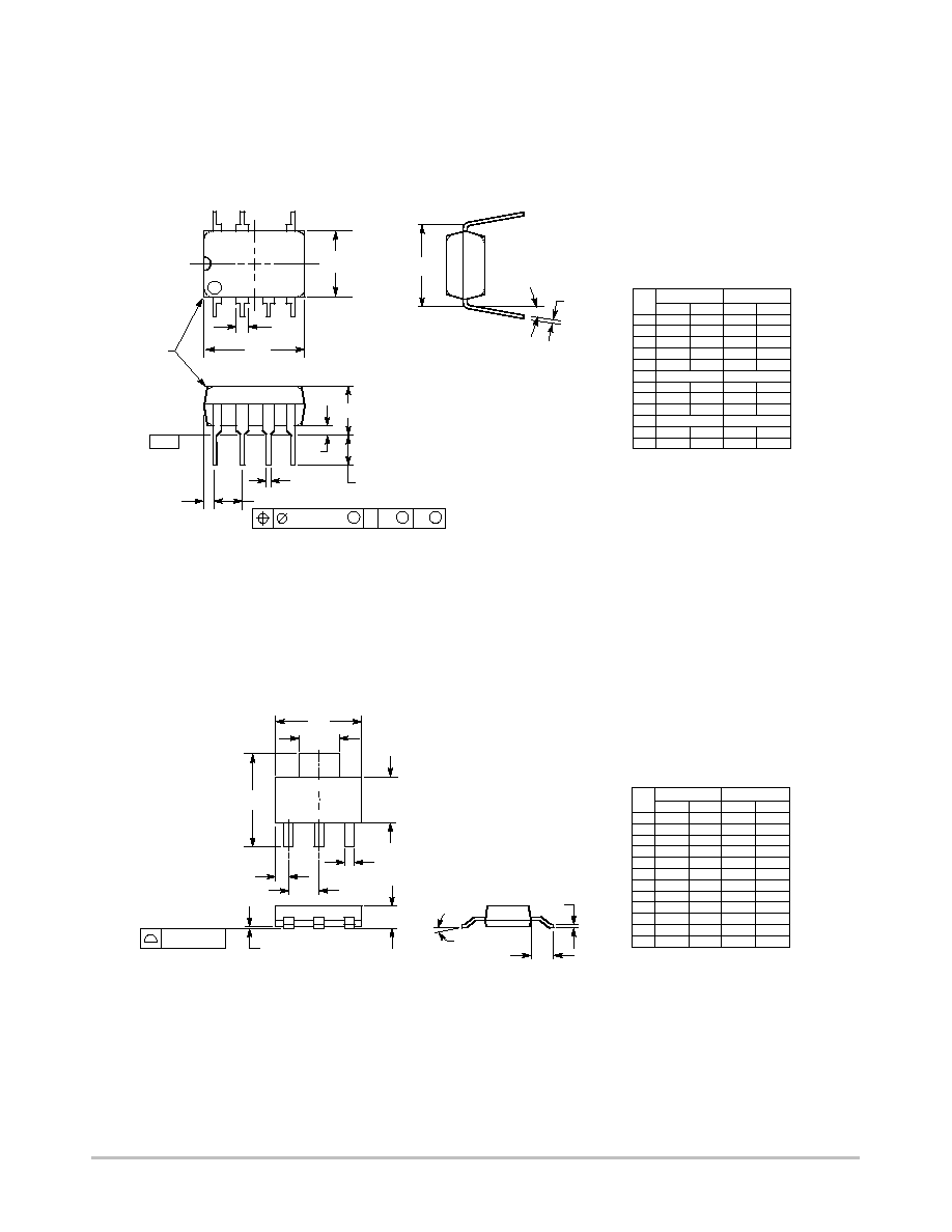
PACKAGE DIMENSIONS
DIP-8
P SUFFIX
CASE 626A-01
ISSUE O
NOTES:
1. DIMENSIONING AND TOLERANCING PER ANSI
Y14.5M, 1982.
2. CONTROLLING DIMENSION: MILLIMETER.
3. PACKAGE CONTOUR OPTIONAL (ROUND OR
SQUARE CORNERS).
4. DIMENSION L TO CENTER OF LEAD WHEN
FORMED PARALLEL.
5. DIMENSIONS A AND B ARE DATUMS.
1
4
5
8
F
NOTE 3
-T-
SEATING
PLANE
H
J
G
D
K
N
C
L
M
M
A
M
0.13 (0.005)
B
M
T
DIM
MIN
MAX
MIN
MAX
INCHES
MILLIMETERS
A
9.40
10.16
0.370
0.400
B
6.10
6.60
0.240
0.260
C
3.94
4.45
0.155
0.175
D
0.38
0.51
0.015
0.020
F
1.02
1.78
0.040
0.070
G
2.54 BSC
0.100 BSC
H
0.76
1.27
0.030
0.050
J
0.20
0.30
0.008
0.012
K
2.92
3.43
0.115
0.135
L
7.62 BSC
0.300 BSC
M
---
10
---
10
N
0.76
1.01
0.030
0.040
_
_
B
A
SOT-223
ST SUFFIX
CASE 318E-04
ISSUE K
H
S
F
A
B
D
G
L
4
1
2
3
0.08 (0003)
C
M
K
J
DIM
A
MIN
MAX
MIN
MAX
MILLIMETERS
0.249
0.263
6.30
6.70
INCHES
B
0.130
0.145
3.30
3.70
C
0.060
0.068
1.50
1.75
D
0.024
0.035
0.60
0.89
F
0.115
0.126
2.90
3.20
G
0.087
0.094
2.20
2.40
H 0.0008 0.0040
0.020
0.100
J
0.009
0.014
0.24
0.35
K
0.060
0.078
1.50
2.00
L
0.033
0.041
0.85
1.05
M
0
10
0
10
S
0.264
0.287
6.70
7.30
NOTES:
1. DIMENSIONING AND TOLERANCING PER ANSI
Y14.5M, 1982.
2. CONTROLLING DIMENSION: INCH.
_
_
_
_

NCP1050, NCP1051, NCP1052, NCP1053, NCP1054, NCP1055
http://onsemi.com
24
ON Semiconductor and are registered trademarks of Semiconductor Components Industries, LLC (SCILLC). SCILLC reserves the right to make
changes without further notice to any products herein. SCILLC makes no warranty, representation or guarantee regarding the suitability of its products for any
particular purpose, nor does SCILLC assume any liability arising out of the application or use of any product or circuit, and specifically disclaims any and all
liability, including without limitation special, consequential or incidental damages. "Typical" parameters which may be provided in SCILLC data sheets and/or
specifications can and do vary in different applications and actual performance may vary over time. All operating parameters, including "Typicals" must be
validated for each customer application by customer's technical experts. SCILLC does not convey any license under its patent rights nor the rights of others.
SCILLC products are not designed, intended, or authorized for use as components in systems intended for surgical implant into the body, or other applications
intended to support or sustain life, or for any other application in which the failure of the SCILLC product could create a situation where personal injury or death
may occur. Should Buyer purchase or use SCILLC products for any such unintended or unauthorized application, Buyer shall indemnify and hold SCILLC
and its officers, employees, subsidiaries, affiliates, and distributors harmless against all claims, costs, damages, and expenses, and reasonable attorney fees
arising out of, directly or indirectly, any claim of personal injury or death associated with such unintended or unauthorized use, even if such claim alleges that
SCILLC was negligent regarding the design or manufacture of the part. SCILLC is an Equal Opportunity/Affirmative Action Employer.
PUBLICATION ORDERING INFORMATION
JAPAN: ON Semiconductor, Japan Customer Focus Center
2-9-1 Kamimeguro, Meguro-ku, Tokyo, Japan 153-0051
Phone: 81-3-5773-3850
ON Semiconductor Website: http://onsemi.com
For additional information, please contact your local
Sales Representative.
NCP1050/D
The products described herein (NCP1050, 1051, 1052, 1053, 1054, 1055), may be covered by one or more of the following U.S. patents:
4,553,084; 5,418,410; 5,477,175; 6,137,696; 6,137,702; 6,271,735, 6,480,043, 6,362,067, 6,587,357. There may be other patents pending.
SENSEFET is a trademark of Semiconductor Components Industries, LLC (SCILLC)
Literature Fulfillment:
Literature Distribution Center for ON Semiconductor
P.O. Box 5163, Denver, Colorado 80217 USA
Phone: 303-675-2175 or 800-344-3860 Toll Free USA/Canada
Fax: 303-675-2176 or 800-344-3867 Toll Free USA/Canada
Email: orderlit@onsemi.com
N. American Technical Support: 800-282-9855 Toll Free USA/Canada