
©
Semiconductor Components Industries, LLC, 2004
July, 2004 - Rev. 4
1
Publication Order Number:
NCP1086/D
NCP1086
1.5 A Adjustable and 3.3 V
Fixed Output Linear
Regulator
The NCP1086 linear regulator provides 1.5 A at 3.3 V or adjustable
output voltage. The adjustable output voltage device uses two external
resistors to set the output voltage within a 1.25 V to 5.5 V range.
The regulators is intended for use as post regulator and
microprocessor supply. The fast loop response and low dropout
voltage make this regulator ideal for applications where low voltage
operation and good transient response are important.
The circuit is designed to operate with dropout voltages less than
1.4 V at 1.5 A output current. Device protection includes overcurrent
and thermal shutdown.
This device is pin compatible with LT1086 family of linear
regulators and has lower dropout voltage.
The regulators are available in TO-220-3, surface mount
D
2
PAK-3, and SOT-223 packages.
Features
∑
Output Current to 1.5 A
∑
Output Accuracy to
±
1% Over Temperature
∑
Dropout Voltage (typical) 1.05 V @ 1.5 A
∑
Fast Transient Response
∑
Fault Protection Circuitry
Current Limit
Thermal Shutdown
∑
Pb-Free Packages are Available*
5.0 V
V
IN
V
OUT
Adj
NCP1086
10
m
F
5.0 V
0.1
m
F
5.0 V
Tantalum
124
W
1.0%
200
W
1.0%
22
m
F
5.0 V
3.3 V
@ 1.5 A
V
IN
V
OUT
GND
NCP1086
10
m
F
5.0 V
22
m
F
5.0 V
3.3 V
@ 1.5 A
Figure 1. Application Diagram, Adjustable Output
Figure 2. Application Diagram, 3.3 V Fixed Output
*For additional information on our Pb-Free strategy and soldering details, please
download the ON Semiconductor Soldering and Mounting Techniques
Reference Manual, SOLDERRM/D.
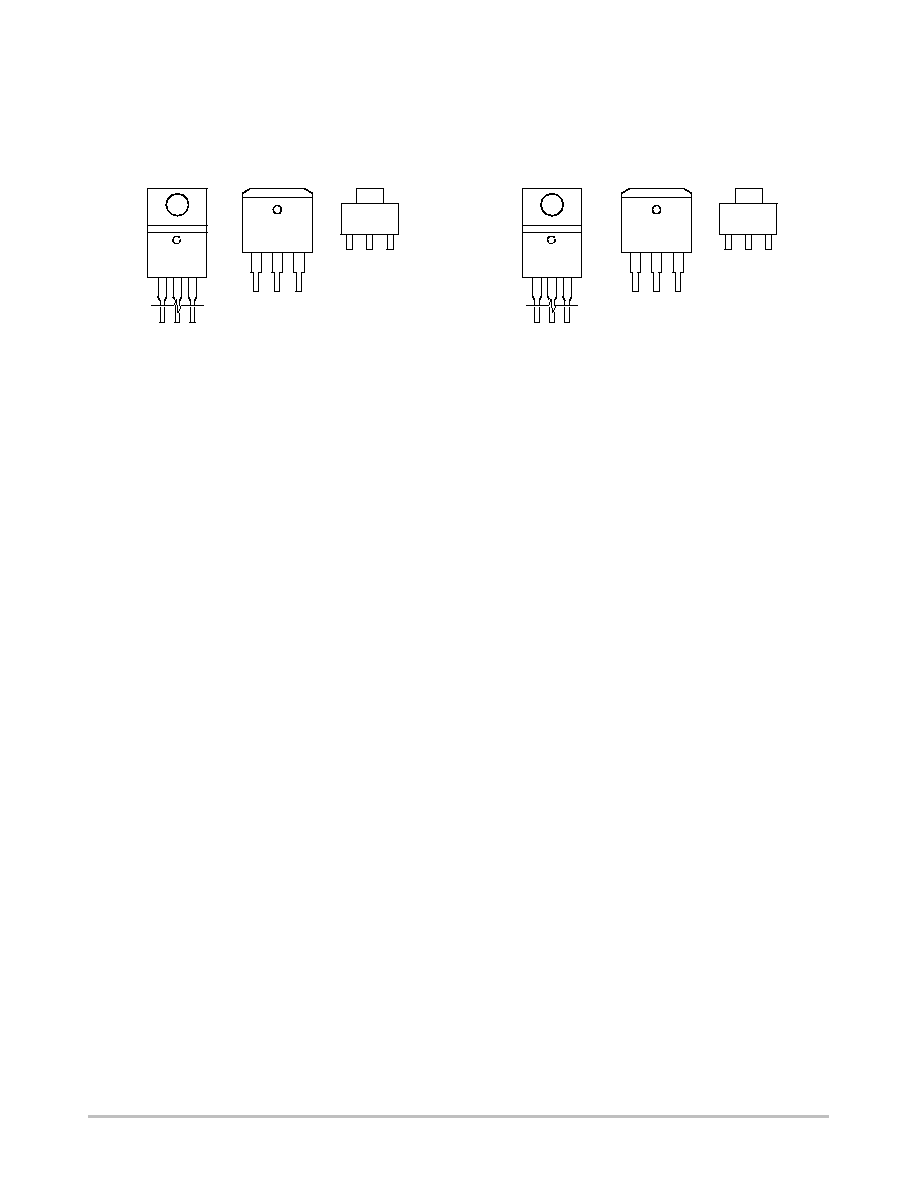
SOT-223
ST SUFFIX
CASE 318E
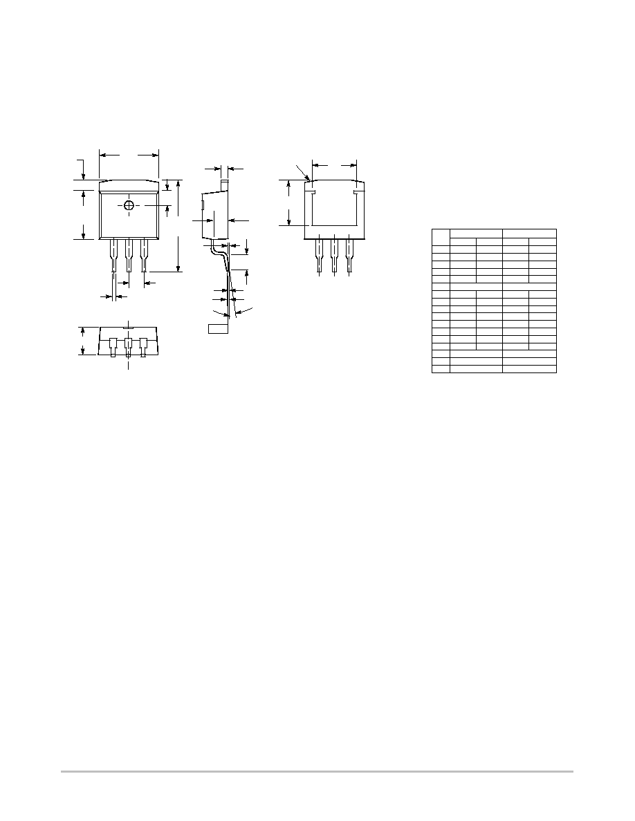
TO-220-3
T SUFFIX
CASE 221A
Tab = V
OUT
Pin 1. Adj
2. V
OUT
3. V
IN
1
2
3
Adjustable
Output
3.3 V Fixed
Output
Tab = V
OUT
Pin 1. GND
2. V
OUT
3. V
IN
See general marking information in the device marking
section on page 10 of this data sheet.
DEVICE MARKING INFORMATION
1
2
3
http://onsemi.com
D
2
PAK-3
DP SUFFIX
CASE 418AB
1
2
3
See detailed ordering and shipping information in the package
dimensions section on page 9 of this data sheet.
ORDERING INFORMATION
NCP1086
http://onsemi.com
2
MAXIMUM RATINGS*
Parameter
Value
Unit
Supply Voltage, V
CC
7.0
V
Operating Temperature Range
-40 to +70
∞
C
Junction Temperature
150
∞
C
Storage Temperature Range
-60 to +150
∞
C
Lead Temperature Soldering:
Wave Solder (through hole styles only) Note 1
Reflow (SMD styles only) Note 2
260 Peak
230 Peak
∞
C
ESD Damage Threshold
2.0
kV
Maximum ratings are those values beyond which device damage can occur. Maximum ratings applied to the device are individual stress limit
values (not normal operating conditions) and are not valid simultaneously. If these limits are exceeded, device functional operation is not implied,
damage may occur and reliability may be affected.
1. 10 second maximum.
2. 60 second maximum above 183
∞
C.
ELECTRICAL CHARACTERISTICS
(C
IN
= 10
m
F, C
OUT
= 22
m
F Tantalum, V
OUT
+ V
DROPOUT
< V
IN
< 7.0 V, 0
∞
C
T
A
70
∞
C,
T
J
+150
∞
C, unless otherwise specified, I
full load
= 1.5 A.)
Characteristic
Test Conditions
Min
Typ
Max
Unit
ADJUSTABLE OUTPUT VOLTAGE
Reference Voltage (Notes 3 and 4)
V
IN
- V
OUT
= 1.5 V; V
Adj
= 0 V,
10 mA
I
OUT
1.5 A
1.241
(-1%)
1.254
1.266
(+1%)
V
Line Regulation
1.5 V
V
IN
- V
OUT
5.75 V; I
OUT
= 10 mA
-
0.02
0.2
%
Load Regulation (Notes 3 and 4)
V
IN
- V
OUT
= 1.5 V; 10 mA
I
OUT
1.5 A
-
0.04
0.4
%
Dropout Voltage (Note 5)
I
OUT
= 1.5 A
-
1.05
1.4
V
Current Limit
V
IN
- V
OUT
= 3.0 V; T
J
25
∞
C
1.6
3.1
-
A
Minimum Load Current (Note 6)
V
IN
= 7.0 V; V
Adj
= 0
-
0.6
2.0
mA
Adjust Pin Current
V
IN
- V
OUT
= 3.0 V; I
OUT
= 10 mA
-
50
100
m
A
Thermal Regulation (Note 7)
30 ms pulse; T
A
= 25
∞
C
-
0.002
0.02
%/W
Ripple Rejection (Note 7)
f = 120 Hz; I
OUT
= 1.5 A; V
IN
- V
OUT
= 3.0 V;
V
RIPPLE
= 1.0 V
P-P
-
80
-
dB
Thermal Shutdown (Note 8)
-
150
180
210
∞
C
Thermal Shutdown Hysteresis (Note 8)
-
-
25
-
∞
C
FIXED OUTPUT VOLTAGE
Output Voltage (Notes 3 and 4)
V
IN
- V
OUT
= 1.5 V, 0
I
OUT
1.5 A
3.25
(-1.5%)
3.3
3.35
(+1.5%)
V
Line Regulation
2.0 V
V
IN
- V
OUT
3.7 V; I
OUT
= 10 mA
-
0.02
0.2
%
Load Regulation (Notes 3 and 4)
V
IN
- V
OUT
= 2.0 V; 10 mA
I
OUT
1.5 A
-
0.04
0.4
%
Dropout Voltage (Note 5)
I
OUT
= 1.5 A
-
1.05
1.4
V
Current Limit
V
IN
- V
OUT
= 3.0 V
1.6
3.1
-
A
Quiescent Current
I
OUT
= 10 mA
-
5.0
10
mA
Thermal Regulation (Note 7)
30 ms pulse; T
A
= 25
∞
C
-
0.002
0.02
%/W
3. Load regulation and output voltage are measured at a constant junction temperature by low duty cycle pulse testing. Changes in output
voltage due to thermal gradients or temperature changes must be taken into account separately.
4. Specifications apply for an external Kelvin sense connection at a point on the output pin 1/4" from the bottom of the package.
5. Dropout voltage is a measurement of the minimum input/output differential at full load.
6. The minimum load current is the minimum current required to maintain regulation. Normally the current in the resistor divider used to set the
output voltage is selected to meet the minimum requirement.
7. Guaranteed by design, not 100% tested in production.
8. Thermal shutdown is 100% functionally tested in production.

NCP1086
http://onsemi.com
3
ELECTRICAL CHARACTERISTICS
(continued) (C
IN
= 10
m
F, C
OUT
= 22
m
F Tantalum, V
OUT
+ V
DROPOUT
< V
IN
< 7.0 V,
0
∞
C
T
A
70
∞
C, T
J
+150
∞
C, unless otherwise specified, I
full load
= 1.5 A.)
Characteristic
Test Conditions
Min
Typ
Max
Unit
FIXED OUTPUT VOLTAGE (continued)
Ripple Rejection (Note 9)
f = 120 Hz; I
OUT
= 1.5 A; V
IN
- V
OUT
= 3.0 V;
V
RIPPLE
= 1.0 V
P-P
-
80
-
dB
Thermal Shutdown (Note 10)
-
150
180
210
∞
C
Thermal Shutdown Hysteresis
(Note 10)
-
-
25
-
∞
C
9. Guaranteed by design, not 100% tested in production.
10. Thermal shutdown is 100% functionally tested in production.
PACKAGE PIN DESCRIPTION, ADJUSTABLE OUTPUT
Package Pin Number
D
2
PAK-3
TO-220-3
SOT-223
Pin Symbol
Function
1
1
1
Adj
Adjust pin (low side of the internal reference).
2
2
2
V
OUT
Regulated output voltage (case).
3
3
3
V
IN
Input voltage.
PACKAGE PIN DESCRIPTION, 3.3 V FIXED OUTPUT
Package Pin Number
D
2
PAK-3
TO-220-3
SOT-223
Pin Symbol
Function
1
1
1
GND
Ground connection.
2
2
2
V
OUT
Regulated output voltage (case).
3
3
3
V
IN
Input voltage.
+
-
Thermal
Shutdown
Bandgap
Output
Current
Limit
Error
Amplifier
V
OUT
Adj
V
IN
+
-
Thermal
Shutdown
Bandgap
Output
Current
Limit
Error
Amplifier
V
OUT
GND
V
IN
Figure 3. Block Diagram, Adjustable Output
Figure 4. Block Diagram, 3.3 V Fixed Output
NCP1086
http://onsemi.com
4
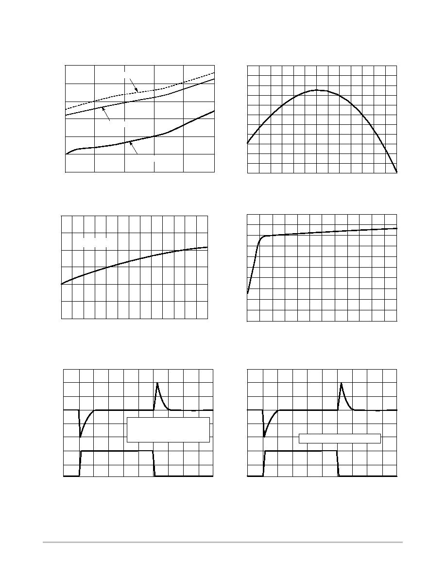
TYPICAL PERFORMANCE CHARACTERISTICS
Figure 5. Dropout Voltage vs. Output Current
0
T
J
(
∞
C)
Figure 6. Reference Voltage vs. Temperature
Output
V
oltage Deviation (%)
0.10
0.08
0.04
0.00
-0.04
-0.08
-0.12
10 20
30 40 50
60 70 80
90 100 110 120 130
0
Temperature (
∞
C)
Figure 7. Adjust Pin Current vs. Temperature
(Adjustable Output)
Adjust
Pin Current (
m
A)
40
45
50
55
60
65
70
20
40
60
80
100
120
I
O
= 10mA
0
300
I
OUT
(mA)
V Drop Out (V)
0.75
T
CASE
= 125
∞
C
T
CASE
= 25
∞
C
T
CASE
= 0
∞
C
600
900
1200
1500
0.80
0.85
0.90
0.95
1.00
1.05
V
IN
- V
OUT
(V)
I
SC
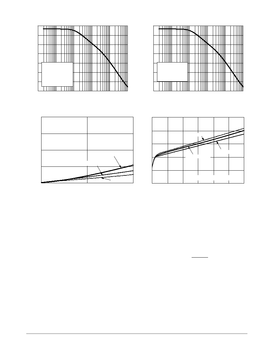
(A)
4.0
3.1
2.7
1.9
1.5
2.3
1.0
2.0
3.0
5.0
6.0
7.0
3.5
Figure 8. Short Circuit Current vs V
IN
- V
OUT
Figure 9. Transient Response (Adjustable Output)
Figure 10. Transient Response (3.3 V Fixed Output)
Time,
m
s
Load Step (mA)
3.0
200
0
1.0
2.0
4.0
5.0
6.0
7.0
8.0
9.0
10
V
oltage Deviation (mV)
100
0
-120
0
-200
1500
750
0
Time,
m
s
Load Step (mA)
3.0
200
0
1.0
2.0
4.0
5.0
6.0
7.0
8.0
9.0
10
V
oltage Deviation (mV)
100
0
-120
0
-200
1500
750
0
V
OUT
= 3.3 V
C
OUT
= C
IN
= 22
m
F Tantalum
C
Adj
= 0.1
m
F
C
OUT
= C
IN
= 22
m
F Tantalum
NCP1086
http://onsemi.com
5
T
CASE
= 0
∞
C
Figure 11. Ripple Rejection vs. Frequency
(Adjustable Output)
0
Output Current (A)
Output V
oltage Deviation, (%)
0.100
T
CASE
= 125
∞
C
T
CASE
= 25
∞
C
1.0
2.0
0.075
0.050
0.025
0
V
IN
- V
OUT
(V)
Minimum Load Current (mA)
4.0
0.60
0.55
0.45
0.40
0.65
0.50
1.0
2.0
3.0
5.0
6.0
7.0
T
CASE
= 25
∞
C
T
CASE
= 125
∞
C
T
CASE
= 0
∞
C
10
1
Frequency (Hz)
Ripple Rejection (dB)
85
75
65
55
45
35
25
15
10
2
10
3
10
4
10
5
10
6
10
1
Frequency (Hz)
Ripple Rejection (dB)
85
75
65
55
45
35
25
15
10
2
10
3
10
4
10
5
10
6
Figure 12. Ripple Rejection vs. Frequency
(3.3 V Fixed Output)
Figure 13. Load Regulation vs. Output Current
(Adjustable Output)
Figure 14. Minimum Load Current vs V
IN
- V
OUT
(Adjustable Output)
T
CASE
= 25
∞
C
I
OUT
= 6A
(V
IN
- V
OUT
= 3V)
V
RIPPLE
= 1.6V
PP
C
Adj
= 0.1
m
F
T
CASE
= 25
∞
C
I
OUT
= 6A
(V
IN
- V
OUT
= 3V)
V
RIPPLE
= 1.6V
PP
C
IN
= C
OUt
= 22
m
F Tantalum
APPLICATIONS INFORMATION
The NCP1086 voltage regulator series provides
adjustable
and 3.3 V output voltages at currents up to 1.5 A.
The regulator is protected against overcurrent conditions
and includes thermal shutdown.
The NCP1086 series has a composite PNP-NPN output
transistor and requires an output capacitor for stability. A
detailed procedure for selecting this capacitor is included in
the Stability Considerations section.
Adjustable Operation
The adjustable output device has an output voltage range
of 1.25 V to 5.5 V. An external resistor divider sets the
output voltage as shown in Figure 15. The regulator
maintains a fixed 1.25 V (typical) reference between the
output pin and the adjust pin.
A resistor divider network R1 and R2 causes a fixed
current to flow to ground. This current creates a voltage
across R2 that adds to the 1.25 V across R1 and sets the
overall output voltage. The adjust pin current (typically
50
mA) also flows through R2 and adds a small error that
should be taken into account if precise adjustment of V
OUT
is necessary.
The output voltage is set according to the formula:
VOUT
+
VREF
R1
)
R2
R1
)
IAdj
R2
The term I
Adj
◊
R2 represents the error added by the adjust
pin current.
R1 is chosen so that the minimum load current is at least
2.0 mA. R1 and R2 should be the same type, e.g. metal film
for best tracking over temperature. While not required, a
bypass capacitor from the adjust pin to ground will improve
ripple rejection and transient response. A 0.1
mF tantalum
capacitor is recommended for "first cut" design. Type and
value may be varied to obtain optimum performance vs
price.
NCP1086
http://onsemi.com
6
C
Adj
I
Adj
Figure 15. Resistor Divider Scheme
V
REF
R
2
R
1
C
2
V
OUT
V
IN
C
1
V
IN
V
OUT
Adj
NCP1086
The adjustable output linear regulator has an absolute
maximum specification of 7.0 V for the voltage difference
between V
IN
and V
OUT
. However, the IC may be used to
regulate voltages in excess of 7.0 V. The main
considerations in such a design are powerup and short circuit
capability.
In most applications, ramp-up of the power supply to V
IN
is fairly slow, typically on the order of several tens of
milliseconds, while the regulator responds in less than one
microsecond. In this case, the linear regulator begins
charging the load as soon as the V
IN
to V
OUT
differential is
large enough that the pass transistor conducts current. The
load at this point is essentially at ground, and the supply
voltage is on the order of several hundred mV, with the result
that the pass transistor is in dropout. As the supply to V
IN
increases, the pass transistor will remain in dropout, and
current is passed to the load until V
OUT
reaches the point at
which the IC is in regulation. Further increase in the supply
voltage brings the pass transistor out of dropout. The result
is that the output voltage follows the power supply ramp-up,
staying in dropout until the regulation point is reached. In
this manner, any output voltage may be regulated. There is
no theoretical limit to the regulated voltage as long as the
V
IN
to V
OUT
differential of 7.0 V is not exceeded.
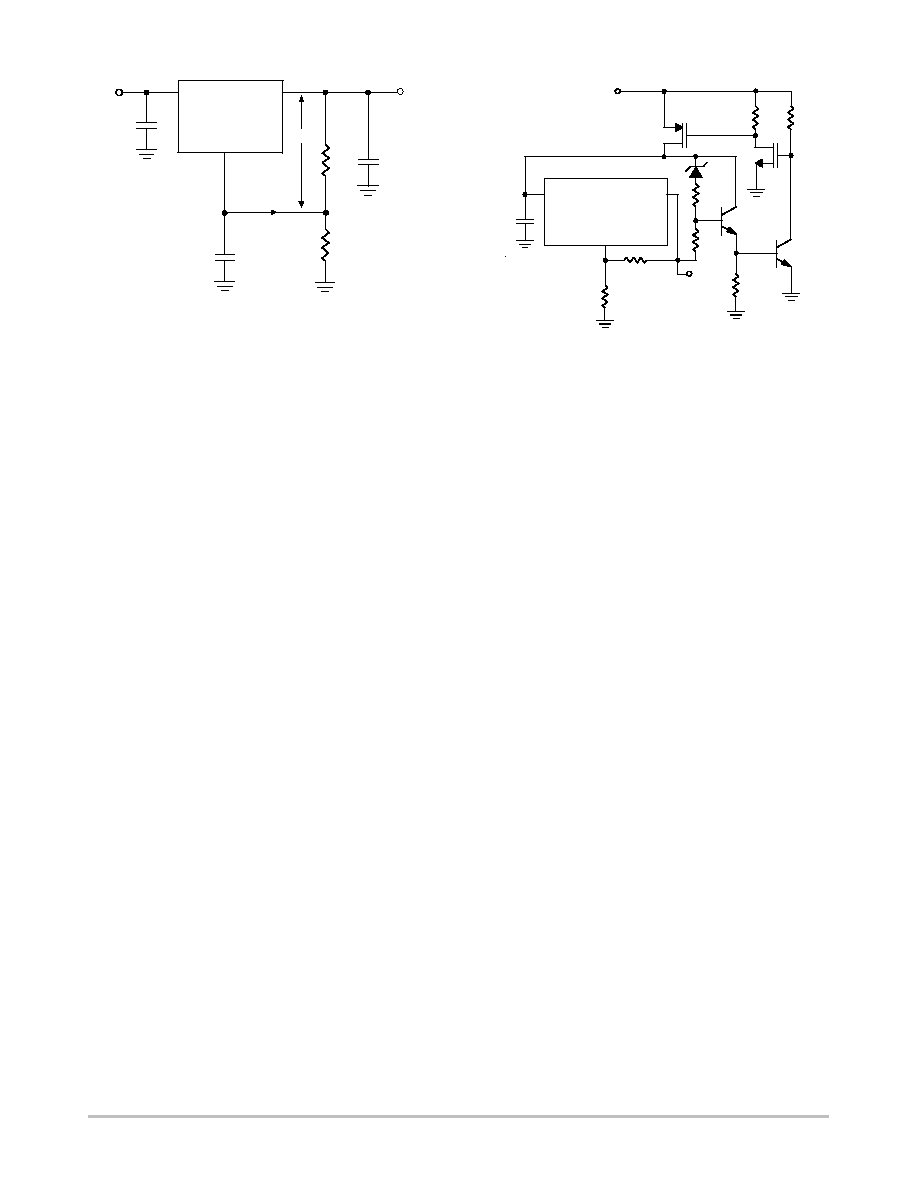
However, the possibility of destroying the IC in a short
circuit condition is very real for this type of design. Short
circuit conditions will result in the immediate operation of
the pass transistor outside of its safe operating area.
Overvoltage stresses will then cause destruction of the pass
transistor before overcurrent or thermal shutdown circuitry
can become active. Additional circuitry may be required to
clamp the V
IN
to V
OUT
differential to less than 7.0 V if
fail-safe operation is required. One possible clamp circuit is
illustrated in Figure 16; however, the design of clamp
circuitry must be done on an application by application
basis. Care must be taken to ensure the clamp actually
protects the design. Components used in the clamp design
must be able to withstand the short circuit condition
indefinitely while protecting the IC.
Figure 16. Short Circuit Protection Circuit for High
Voltage Application
V
IN
V
OUT
Adj
NCP1086
V
OUT
EXTERNAL
SUPPLY
Stability Considerations
The output or compensation capacitor helps determine
three main characteristics of a linear regulator: startup delay,
load transient response and loop stability.
The capacitor value and type is based on cost, availability,
size and temperature constraints. A tantalum or aluminum
electrolytic capacitor is best, since a film or ceramic
capacitor with almost zero ESR can cause instability. The
aluminum electrolytic capacitor is the least expensive
solution. However, when the circuit operates at low
temperatures, both the value and ESR of the capacitor will
vary considerably. The capacitor manufacturers' data sheet
provides this information.
A 22
mF tantalum capacitor will work for most
applications, but with high current regulators such as the
NCP1086 series the transient response and stability improve
with higher values of capacitance. The majority of
applications for this regulator involve large changes in load
current, so the output capacitor must supply the
instantaneous
load current. The ESR of the output capacitor
causes an immediate drop in output voltage given by:
D
V
+ D
I
ESR
For microprocessor applications it is customary to use an
output capacitor network consisting of several tantalum and
ceramic capacitors in parallel. This reduces the overall ESR
and reduces the instantaneous output voltage drop under
load transient conditions. The output capacitor network
should be as close as possible to the load for the best results.
NCP1086
http://onsemi.com
7
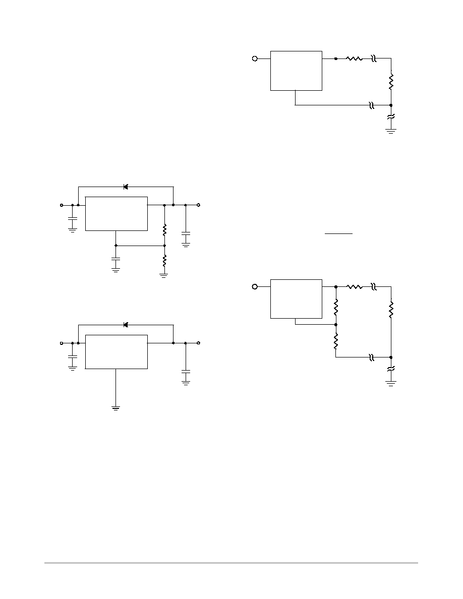
Protection Diodes
When large external capacitors are used with a linear
regulator it is sometimes necessary to add protection diodes.
If the input voltage of the regulator gets shorted, the output
capacitor will discharge into the output of the regulator. The
discharge current depends on the value of the capacitor, the
output voltage and the rate at which V
IN
drops. In the
NCP1086 series linear regulator, the discharge path is
through a large junction and protection diodes are not
usually needed. If the regulator is used with large values of
output capacitance and the input voltage is instantaneously
shorted to ground, damage can occur. In this case, a diode
connected as shown in Figure 17 or Figure 18 is
recommended.
Figure 17. Protection Diode Scheme for Large Output
Capacitors (Adjustable Output)
C
2
V
OUT
V
IN
C
1
V
IN
V
OUT
Adj
NCP1086
IN4002 (optional)
C
Adj
R
1
R
2
Figure 18. Protection Diode Scheme for Large Output
Capacitors (3.3 V Fixed Output)
C
2
V
OUT
V
IN
C
1
V
IN
V
OUT
GND
NCP1086
IN4002 (optional)
Output Voltage Sensing
Since the NCP1086 is a three terminal regulator, it is not
possible to provide true remote load sensing. Load
regulation is limited by the resistance of the conductors
connecting the regulator to the load.
For best results the fixed output regulator should be
connected as shown in Figure 19.
Figure 19. Conductor Parasitic Resistance Effects
Can Be Minimized with the Above Grounding
Scheme for Fixed Output Regulators
V
IN
V
IN
V
OUT
NCP1086
Conductor Parasitic
Resistance
R
LOAD
R
C
For the adjustable regulator, the best load regulation
occurs when R1 is connected directly to the output pin of the
regulator as shown in Figure 20. If R1 is connected to the
load, R
C
is multiplied by the divider ratio and the effective
resistance between the regulator and the load becomes
RC
R1
)
R2
R1
where R
C
= conductor parasitic resistance.
Figure 20. Grounding Scheme for the
Adjustable Output Regulator to Minimize
Parasitic Resistance Effects
V
IN
V
IN
V
OUT
Adj
NCP1086
Conductor Parasitic
Resistance
R
1
R
LOAD
R
2
R
C
Calculating Power Dissipation and
Heatsink Requirements
The NCP1086 linear regulator includes thermal shutdown
and current limit circuitry to protect the device. High power
regulators such as these usually operate at high junction
temperatures so it is important to calculate the power
dissipation and junction temperatures accurately to ensure
that an adequate heatsink is used.

NCP1086
http://onsemi.com
8
The case is connected to V
OUT
, and electrical isolation
may be required for some applications. Thermal compound
should always be used with high current regulators such as
these.
The thermal characteristics of an IC depend on the
following four factors:
1.
Maximum Ambient Temperature T
A
(
∞
C)
2.
Power dissipation P
D
(W)
3.
Maximum junction temperature T
J
(
∞
C)
4.
Thermal resistance junction to ambient R
qJA
(
∞
C/W)
These four are related by the equation
TJ
+
TA
)
PD
R
Q
JA
(eq. 1)
The maximum ambient temperature and the power
dissipation are determined by the design while the
maximum junction temperature and the thermal resistance
depend on the manufacturer and the package type.
The maximum power dissipation for a regulator is:
PD(max)
+
{VIN(max)
*
VOUT(min)}IOUT(max)
)
VIN(max)IQ
(eq. 2)
where:
V
IN(max)
is the maximum input voltage,
V
OUT(min)
is the minimum output voltage,
I
OUT(max)
is the maximum output current, for the application
I
Q
is the maximum quiescent current at I
OUT(max)
.
A heatsink effectively increases the surface area of the
package to improve the flow of heat away from the IC and
into the surrounding air.
Each material in the heat flow path between the IC and the
outside environment has a thermal resistance. Like series
electrical resistances, these resistances are summed to
determine R
qJA
, the total thermal resistance between the
junction and the surrounding air.
1.
Thermal Resistance of the junction to case, R
qJC
(
∞
C/W)
2.
Thermal Resistance of the case to Heatsink, R
qCS
(
∞
C/W)
3.
Thermal Resistance of the Heatsink to the ambient
air, R
qSA
(
∞
C/W)
These are connected by the equation:
R
Q
JA
+
R
Q
JC
)
R
Q
CS
)
R
Q
SA
(eq. 3)
The value for R
qJA
is calculated using Equation 3 and the
result can be substituted in Equation 1.
The value for R
qJC
is 3.5
∞
C/W. For a high current
regulator such as the NCP1086 the majority of the heat is
generated in the power transistor section. The value for
R
qSA
depends on the heatsink type, while R
qCS
depends on
factors such as package type, heatsink interface (is an
insulator and thermal grease used?), and the contact area
between the heatsink and the package. Once these
calculations are complete, the maximum permissible value
of R
qJA
can be calculated and the proper heatsink selected.
For further discussion on heatsink selection, see application
note "Thermal Management," document number
AND8036/D via our website at www.onsemi.com.
NCP1086
http://onsemi.com
9
ORDERING INFORMATION
Device
Type
Package
Shipping
NCP1086T-ADJ
Adjustable
TO-220-3
50 Units/Rail
NCP1086D2T-ADJ
Adjustable
D
2
PAK-3
50 Units/Rail
NCP1086D2T-ADJR4
Adjustable
D
2
PAK-3
750 Tape & Reel
NCP1086D2T-ADJR4G
Adjustable
D
2
PAK-3
(Pb-Free)
750 Tape & Reel
NCP1086ST-ADJT3
Adjustable
SOT-223
2500 Tape & Reel
NCP1086T-33
3.3 V
TO-220-3
50 Units/Rail
NCP1086D2T-33
3.3 V
D
2
PAK-3
50 Units/Rail
NCP1086D2T-33R4
3.3 V
D
2
PAK-3
750 Tape & Reel
NCP1086D2T-33R4G
3.3 V
D
2
PAK-3
(Pb-Free)
750 Tape & Reel
NCP1086ST-33T3
3.3 V
SOT-223
2500 Tape & Reel
For information on tape and reel specifications, including part orientation and tape sizes, please refer to our Tape and Reel Packaging
Specifications Brochure, BRD8011/D.
NCP1086
http://onsemi.com
10
MARKING DIAGRAMS
NCP1086-A
AWLYWW
1
A
= Assembly Location
WL, L
= Wafer Lot
YY, Y
= Year
WW, W = Work Week
AYW
086-A
1
NCP1086-A
AWLYWW
1
D
2
PAK-3
D2T SUFFIX
CASE 418AB
SOT-223
ST SUFFIX
CASE 318E
TO-220-3
T SUFFIX
CASE 221A
1086-33
AWLYWW
1
TO-220-3
T SUFFIX
CASE 221A
1086-33
AWLYWW
1
D
2
PAK-3
D2T SUFFIX
CASE 418AB
AYW
08633
1
SOT-223
ST SUFFIX
CASE 318E
3.3 V Fixed Output
Adjustable Output
NCP1086
http://onsemi.com
11
PACKAGE DIMENSIONS
TO-220-3
T SUFFIX
CASE 221A-08
ISSUE AA
NOTES:
1. DIMENSIONING AND TOLERANCING PER ANSI
Y14.5M, 1982.
2. CONTROLLING DIMENSION: INCH.
A
K
L
G
D
N
H
Q
F
1 2 3
4
-T-
SEATING
PLANE
S
R
J
U
T
C
3 PL
-B-
-Y-
M
B
M
0.25 (0.010)
Y
DIM
MIN
MAX
MIN
MAX
MILLIMETERS
INCHES
A
0.560
0.625
14.23
15.87
B
0.380
0.420
9.66
10.66
C
0.140
0.190
3.56
4.82
D
0.025
0.035
0.64
0.89
F
0.139
0.155
3.53
3.93
G
0.100 BSC
2.54 BSC
H
---
0.280
---
7.11
J
0.012
0.045
0.31
1.14
K
0.500
0.580
12.70
14.73
L
0.045
0.060
1.15
1.52
N
0.200 BSC
5.08 BSC
Q
0.100
0.135
2.54
3.42
R
0.080
0.115
2.04
2.92
S
0.020
0.055
0.51
1.39
T
0.235
0.255
5.97
6.47
U
0.000
0.050
0.00
1.27
V
V
0.045
---
1.15
---
NCP1086
http://onsemi.com
12
PACKAGE DIMENSIONS
D
2
PAK-3
CASE 418AB-01
ISSUE O
NOTES:
1. DIMENSIONS AND TOLERANCING PER
ANSI Y14.5M, 1982.
2. CONTROLLING DIMENSION: INCH.
3. PACKAGE OUTLINE EXCLUSIVE OF MOLD
FLASH AND METAL BURRS.
4. PACKAGE OUTLINE INCLUSIVE OF
PLATING THICKNESS.
5. FOOT LENGTH MEASURED AT INTERCEPT
POINT BETWEEN DATUM A AND LEAD
SURFACE.
A
C
B
S
K
E
M
P
N
D
G
H
W
R
-A-
U
V
TERMINAL 4
DIM
MIN
MAX
MIN
MAX
MILLIMETERS
INCHES
A
0.396
0.406
10.05
10.31
B
0.330
0.340
8.38
8.64
C
0.170
0.180
4.31
4.57
D
0.026
0.036
0.66
0.91
E
0.045
0.055
1.14
1.40
G
0.100 REF
2.54 REF
H
0.580
0.620
14.73
15.75
K
0.055
0.066
1.40
1.68
L
0.000
0.010
0.00
0.25
M
0.098
0.108
2.49
2.74
N
0.017
0.023
0.43
0.58
P
0.090
0.110
2.29
2.79
R
0
8
S
0.095
0.105
2.41
2.67
U
0.30 REF
7.62 REF
V
0.305 REF
7.75 REF
W
0.010
0.25
∞
∞
0
8
∞
∞
L
NCP1086
http://onsemi.com
13
PACKAGE DIMENSIONS
H
S
F
A
B
D
G
L
4
1
2
3
0.08 (0003)
C
M
K
J
DIM
A
MIN
MAX
MIN
MAX
MILLIMETERS
0.249
0.263
6.30
6.70
INCHES
B
0.130
0.145
3.30
3.70
C
0.060
0.068
1.50
1.75
D
0.024
0.035
0.60
0.89
F
0.115
0.126
2.90
3.20
G
0.087
0.094
2.20
2.40
H 0.0008 0.0040
0.020
0.100
J
0.009
0.014
0.24
0.35
K
0.060
0.078
1.50
2.00
L
0.033
0.041
0.85
1.05
M
0
10
0
10
S
0.264
0.287
6.70
7.30
NOTES:
6. DIMENSIONING AND TOLERANCING PER ANSI
Y14.5M, 1982.
7. CONTROLLING DIMENSION: INCH.
_
_
_
_
SOT-223
ST SUFFIX
CASE 318E-04
ISSUE K
1.5
0.059
mm
inches
SCALE 6:1
3.8
0.15
2.0
0.079
6.3
0.248
2.3
0.091
2.3
0.091
2.0
0.079
SOLDERING FOOTPRINT
PACKAGE THERMAL DATA
Parameter
TO-220-3
D
2
PAK-3
SOT-223
Unit
R
q
JC
Typical
3.5
3.5
15
∞
C/W
R
q
JA
Typical
50
10-50*
156
∞
C/W
* Depending on thermal properties of substrate. R
q
JA
= R
q
JC
+ R
q
CA

NCP1086
http://onsemi.com
14
ON Semiconductor and are registered trademarks of Semiconductor Components Industries, LLC (SCILLC). SCILLC reserves the right to make changes without further notice
to any products herein. SCILLC makes no warranty, representation or guarantee regarding the suitability of its products for any particular purpose, nor does SCILLC assume any liability
arising out of the application or use of any product or circuit, and specifically disclaims any and all liability, including without limitation special, consequential or incidental damages.
"Typical" parameters which may be provided in SCILLC data sheets and/or specifications can and do vary in different applications and actual performance may vary over time. All
operating parameters, including "Typicals" must be validated for each customer application by customer's technical experts. SCILLC does not convey any license under its patent rights
nor the rights of others. SCILLC products are not designed, intended, or authorized for use as components in systems intended for surgical implant into the body, or other applications
intended to support or sustain life, or for any other application in which the failure of the SCILLC product could create a situation where personal injury or death may occur. Should
Buyer purchase or use SCILLC products for any such unintended or unauthorized application, Buyer shall indemnify and hold SCILLC and its officers, employees, subsidiaries, affiliates,
and distributors harmless against all claims, costs, damages, and expenses, and reasonable attorney fees arising out of, directly or indirectly, any claim of personal injury or death
associated with such unintended or unauthorized use, even if such claim alleges that SCILLC was negligent regarding the design or manufacture of the part. SCILLC is an Equal
Opportunity/Affirmative Action Employer. This literature is subject to all applicable copyright laws and is not for resale in any manner.
PUBLICATION ORDERING INFORMATION
N. American Technical Support: 800-282-9855 Toll Free
USA/Canada
Japan: ON Semiconductor, Japan Customer Focus Center
2-9-1 Kamimeguro, Meguro-ku, Tokyo, Japan 153-0051
Phone: 81-3-5773-3850
NPC1086/D
LITERATURE FULFILLMENT:
Literature Distribution Center for ON Semiconductor
P.O. Box 61312, Phoenix, Arizona 85082-1312 USA
Phone: 480-829-7710 or 800-344-3860 Toll Free USA/Canada
Fax: 480-829-7709 or 800-344-3867 Toll Free USA/Canada
Email: orderlit@onsemi.com
ON Semiconductor Website: http://onsemi.com
Order Literature: http://www.onsemi.com/litorder
For additional information, please contact your
local Sales Representative.