
©
Semiconductor Components Industries, LLC, 2004
July, 2004 - Rev. 11
1
Publication Order Number:
NCP1117/D
NCP1117, NCV1117
1.0 A Low-Dropout Positive
Fixed and Adjustable
Voltage Regulators
The NCP1117 series are low dropout positive voltage regulators that
are capable of providing an output current that is in excess of 1.0 A
with a maximum dropout voltage of 1.2 V at 800 mA over
temperature. This series contains eight fixed output voltages of 1.5 V,
1.8 V, 2.0 V, 2.5 V, 2.85 V, 3.3 V, 5.0 V, and 12 V that have no
minimum load requirement to maintain regulation. Also included is an
adjustable output version that can be programmed from 1.25 V to
18.8 V with two external resistors. On chip trimming adjusts the
reference/output voltage to within
±
1.0% accuracy. Internal protection
features consist of output current limiting, safe operating area
compensation, and thermal shutdown. The NCP1117 series can
operate with up to 20 V input. Devices are available in SOT-223 and
DPAK packages.
Features
∑
Output Current in Excess of 1.0 A
∑
1.2 V Maximum Dropout Voltage at 800 mA Over Temperature
∑
Fixed Output Voltages of 1.5 V, 1.8 V, 2.0 V, 2.5 V, 2.85 V, 3.3 V,
5.0 V, and 12 V
∑
Adjustable Output Voltage Option
∑
No Minimum Load Requirement for Fixed Voltage Output Devices
∑
Reference/Output Voltage Trimmed to
±
1.0%
∑
Current Limit, Safe Operating and Thermal Shutdown Protection
∑
Operation to 20 V Input
∑
NCV Prefix for Automotive and Other Applications Requiring Site
and Control Changes
∑
Pb-Free Packages are Available
Applications
∑
Consumer and Industrial Equipment Point of Regulation
∑
Active SCSI Termination for 2.85 V Version
∑
Switching Power Supply Post Regulation
∑
Hard Drive Controllers
∑
Battery Chargers
10
m
F
1
2
Output
10
m
F
3
Input
NCP1117
XTXX
+
+
Figure 1. Fixed
Output Regulator
10
m
F
1
2 Output
10
m
F
3
Input
NCP1117
XTA
+
+
Figure 2. Adjustable
Output Regulator
22
m
F
1
2
10
m
F
3
NCP1117
XT285
+
+
110
W
110
W
110
W
110
W
4.75 V
to
5.25 V
+
18 to 27
Lines
Figure 3. Active SCSI Bus Terminator
TYPICAL APPLICATIONS
SOT-223
ST SUFFIX
CASE 318H
1
3
DPAK
DT SUFFIX
CASE 369C
Pin: 1. Adjust/Ground
2. Output
3. Input
1
3
Heatsink tab is connected to Pin 2.
See detailed ordering and shipping information in the package
dimensions section on pages 11 and 12 of this data sheet.
ORDERING INFORMATION
See general marking information in the device marking
section on page 13 of this data sheet.
DEVICE MARKING INFORMATION
1 2 3
1
2
3
Tab
Tab
(Top View)
(Top View)
http://onsemi.com

NCP1117, NCV1117
http://onsemi.com
2
MAXIMUM RATINGS
Rating
Symbol
Value
Unit
Input Voltage (Note 1)
V
in
20
V
Output Short Circuit Duration (Notes 2 and 3)
-
Infinite
-
Power Dissipation and Thermal Characteristics
Case 318H (SOT-223)
Power Dissipation (Note 2)
Thermal Resistance, Junction-to-Ambient, Minimum Size Pad
Thermal Resistance, Junction-to-Case
Case 369A (DPAK)
Power Dissipation (Note 2)
Thermal Resistance, Junction-to-Ambient, Minimum Size Pad
Thermal Resistance, Junction-to-Case
P
D
R
q
JA
R
q
JC
P
D
R
q
JA
R
q
JC
Internally Limited
160
15
Internally Limited
67
6.0
W
∞
C/W
∞
C/W
W
∞
C/W
∞
C/W
Maximum Die Junction Temperature Range
T
J
-55 to 150
∞
C
Storage Temperature Range
T
stg
-65 to 150
∞
C
Operating Ambient Temperature Range
NCP1117
NCV1117
T
A
0 to +125
-40 to +125
∞
C
Maximum ratings are those values beyond which device damage can occur. Maximum ratings applied to the device are individual stress limit
values (not normal operating conditions) and are not valid simultaneously. If these limits are exceeded, device functional operation is not implied,
damage may occur and reliability may be affected.
1. This device series contains ESD protection and exceeds the following tests:
Human Body Model 2000 V per MIL-STD-883, Method 3015.
Machine Model Method 200 V.
2. Internal thermal shutdown protection limits the die temperature to approximately 175
∞
C. Proper heatsinking is required to prevent activation.
The maximum package power dissipation is:
PD
+
TJ(max)
*
TA
R
q
JA
3. The regulator output current must not exceed 1.0 A with V
in
greater than 12 V.
NCP1117, NCV1117
http://onsemi.com
3
ELECTRICAL CHARACTERISTICS
(C
in
= 10
m
F, C
out
= 10
m
F, for typical value T
A
= 25
∞
C, for min and max values T
A
is the
operating ambient temperature range that applies unless otherwise noted. (Note 6)
Characteristic
Symbol
Min
Typ
Max
Unit
Reference Voltage, Adjustable Output Devices
(V
in
≠V
out
= 2.0 V, I
out
= 10 mA, T
A
= 25
∞
C)
(V
in
≠V
out
= 1.4 V to 10 V, I
out
= 10 mA to 800 mA) (Note 6)
V
ref
1.238
1.225
1.25
-
1.262
1.270
V
Output Voltage, Fixed Output Devices
1.5 V
(V
in
= 3.5 V, I
out
= 10 mA, T
A
= 25
∞
C)
(V
in
= 2.9 V to 11.5 V, I
out
= 0 mA to 800 mA) (Note 6)
1.8 V
(V
in
= 3.8 V, I
out
= 10 mA, T
A
= 25
∞
C)
(V
in
= 3.2 V to 11.8 V, I
out
= 0 mA to 800 mA) (Note 6)
2.0 V
(V
in
= 4.0 V, I
out
= 10 mA, T
A
= 25
∞
C)
(V
in
= 3.4 V to 12 V, I
out
= 0 mA to 800 mA) (Note 6)
2.5 V
(V
in
= 4.5 V, I
out
= 10 mA, T
A
= 25
∞
C)
(V
in
= 3.9 V to 10 V, I
out
= 0 mA to 800 mA,) (Note 6)
2.85 V (V
in
= 4.85 V, I
out
= 10 mA, T
A
= 25
∞
C)
(V
in
= 4.25 V to 10 V, I
out
= 0 mA to 800 mA) (Note 6)
(V
in
= 4.0 V, I
out
= 0 mA to 500 mA) (Note 6)
3.3 V
(V
in
= 5.3 V, I
out
= 10 mA, T
A
= 25
∞
C)
(V
in
= 4.75 V to 10 V, I
out
= 0 mA to 800 mA) (Note 6)
5.0 V
(V
in
= 7.0 V, I
out
= 10 mA, T
A
= 25
∞
C)
(V
in
= 6.5 V to 12 V, I
out
= 0 mA to 800 mA) (Note 6)
12 V
(V
in
= 14 V, I
out
= 10 mA, T
A
= 25
∞
C)
(V
in
= 13.5 V to 20 V, I
out
= 0 mA to 800 mA) (Note 6)
V
out
1.485
1.470
1.782
1.755
1.970
1.960
2.475
2.450
2.821
2.790
2.790
3.267
3.235
4.950
4.900
11.880
11.760
1.500
-
1.800
-
2.000
-
2.500
-
2.850
-
-
3.300
-
5.000
-
12.000
-
1.515
1.530
1.818
1.845
2.030
2.040
2.525
2.550
2.879
2.910
2.910
3.333
3.365
5.050
5.100
12.120
12.240
V
Line Regulation (Note 4)
Adjustable (V
in
= 2.75 V to 16.25 V, I
out
= 10 mA)
Reg
line
-
0.04
0.1
%
1.5 V
(V
in
= 2.9 V to 11.5 V, I
out
= 0 mA)
1.8 V
(V
in
= 3.2 V to 11.8 V, I
out
= 0 mA)
2.0 V
(V
in
= 3.4 V to 12 V, I
out
= 0 mA)
2.5 V
(V
in
= 3.9 V to 10 V, I
out
= 0 mA)
2.85 V (V
in
= 4.25 V to 10 V, I
out
= 0 mA)
3.3 V
(V
in
= 4.75 V to 15 V, I
out
= 0 mA)
5.0 V
(V
in
= 6.5 V to 15 V, I
out
= 0 mA)
12 V
(V
in
= 13.5 V to 20 V, I
out
= 0 mA)
-
-
-
-
-
-
-
-
0.3
0.4
0.5
0.5
0.8
0.8
0.9
1.0
1.0
1.0
2.5
2.5
3.0
4.5
6.0
7.5
mV
Load Regulation (Note 4)
Adjustable (I
out
= 10 mA to 800 mA, V
in
= 4.25 V)
Reg
line
-
0.2
0.4
%
1.5 V
(I
out
= 0 mA to 800 mA, V
in
= 2.9 V)
1.8 V
(I
out
= 0 mA to 800 mA, V
in
= 3.2 V)
2.0 V
(I
out
= 0 mA to 800 mA, V
in
= 3.4 V)
2.5 V
(I
out
= 0 mA to 800 mA, V
in
= 3.9 V)
2.85 V (I
out
= 0 mA to 800 mA, V
in
= 4.25 V)
3.3 V
(I
out
= 0 mA to 800 mA, V
in
= 4.75 V)
5.0 V
(I
out
= 0 mA to 800 mA, V
in
= 6.5 V)
12 V
(I
out
= 0 mA to 800 mA, V
in
= 13.5 V)
-
-
-
-
-
-
-
-
2.3
2.6
3.0
3.3
3.8
4.3
6.7
16
5.5
6.0
6.0
7.5
8.0
10
15
28
mV
Dropout Voltage (Measured at V
out
- 100 mV)
(I
out
= 100 mA)
(I
out
= 500 mA)
(I
out
= 800 mA)
V
in
-V
out
-
-
-
0.95
1.01
1.07
1.10
1.15
1.20
V
Output Current Limit (V
in
-V
out
= 5.0 V, T
A
= 25
∞
C, Note 5)
I
out
1000
1500
2200
mA
4. Low duty cycle pulse techniques are used during testing to maintain the junction temperature as close to ambient as possible.
5. The regulator output current must not exceed 1.0 A with V
in
greater than 12 V.
6. NCP1117: T
low
= 0
∞
C ,
T
high
= 125
∞
C
NCV1117: T
low
= -40
∞
C, T
high
= 125
∞
C

NCP1117, NCV1117
http://onsemi.com
4
ELECTRICAL CHARACTERISTICS
(C
in
= 10
m
F, C
out
= 10
m
F, for typical value T
A
= 25
∞
C, for min and max values T
A
is the
operating ambient temperature range that applies unless otherwise noted. (Note 7)
Characteristic
Symbol
Min
Typ
Max
Unit
Minimum Required Load Current for Regulation, Adjustable Output Devices
(V
in
= 15 V)
I
L(min)
-
0.8
5.0
mA
Quiescent Current
1.5 V
(V
in
= 11.5 V)
1.8 V
(V
in
= 11.8 V)
2.0 V
(V
in
= 12 V)
2.5 V
(V
in
= 10 V)
2.85 V (V
in
= 10 V)
3.3 V
(V
in
= 15 V)
5.0 V
(V
in
= 15 V)
12 V
(V
in
= 20 V)
I
Q
-
-
-
-
-
-
-
-
3.6
4.2
4.5
5.2
5.5
6.0
6.0
6.0
10
10
10
10
10
10
10
10
mA
Thermal Regulation (T
A
= 25
∞
C, 30 ms Pulse)
-
0.01
0.1
%/W
Ripple Rejection (V
in
-V
out
= 6.4 V, I
out
= 500 mA, 10 V
pp
120 Hz Sinewave)
Adjustable
1.5 V
1.8 V
2.0 V
2.5 V
2.85 V
3.3 V
5.0 V
12 V
RR
67
66
64
64
62
62
60
57
50
73
72
70
70
68
68
64
61
54
-
-
-
-
-
-
-
-
-
dB
Adjustment Pin Current (V
in
= 11.25 V, I
out
= 800 mA)
I
adj
-
52
120
m
A
Adjust Pin Current Change
(V
in
-V
out
= 1.4 V to 10 V, I
out
= 10 mA to 800 mA)
D
I
adj
-
0.4
5.0
m
A
Temperature Stability
S
T
-
0.5
-
%
Long Term Stability (T
A
= 25
∞
C, 1000 Hrs End Point Measurement)
S
t
-
0.3
-
%
RMS Output Noise (f = 10 Hz to 10 kHz)
N
-
0.003
-
%V
out
7. NCP1117: T
low
= 0
∞
C ,
T
high
= 125
∞
C
NCV1117: T
low
= -40
∞
C, T
high
= 125
∞
C

NCP1117, NCV1117
http://onsemi.com
5
V
in
- V
out
, DROPOUT VOL
T
AGE (V)
T
A
, AMBIENT TEMPERATURE (
∞
C)
I
adj
, ADJUST PIN CURRENT (
m
A)
I
out
= 10 mA
0
20
40
60
80
100
Figure 4. Output Voltage Change
vs. Temperature
Figure 5. Dropout Voltage
vs. Output Current
Figure 6. Output Short Circuit Current
vs. Differential Voltage
Figure 7. Output Short Circuit Current
vs. Temperature
Figure 8. Adjust Pin Current
vs. Temperature
Figure 9. Quiescent Current Change
vs. Temperature
0
0.5
1.0
1.5
2.0
0
2
4
6
8
10
12
14
16
18
20
Load pulsed at 1.0% duty cycle
V
in
- V
out
, VOLTAGE DIFFERENTIAL (V)
I
out
, OUTPUT CURRENT (A)
T
J
= 25
∞
C
0
0.2
0.4
0.6
0.8
1.0
1.2
1.4
0
200
400
600
800
1000
Load pulsed at 1.0% duty cycle
I
out
, OUTPUT CURRENT (mA)
T
J
= -40
∞
C
T
J
= 25
∞
C
T
J
= 125
∞
C
V
out
, OUTPUT VOL
T
AGE CHANGE (%)
-2.0
-1.5
-1.0
-0.5
0
0.5
1.0
1.5
2.0
-50
-25
0
25
50
75
100
125
150
T
A
, AMBIENT TEMPERATURE (
∞
C)
V
in
= V
out
+ 3.0 V
I
out
= 10 mA
Adj, 1.5 V,
1.8 V, 2.0 V,
2.5 V
2.85 V, 3.3 V,
5.0 V, 12.0 V
1.0
1.2
1.4
1.6
1.8
2.0
-50
-25
0
25
50
75
100
125
150
-20
-15
-10
-5.0
0
5.0
10
-50
-25
0
25
50
75
100
125
150
T
A
, AMBIENT TEMPERATURE (
∞
C)
I
out
, OUTPUT CURRENT (A)
V
in
= 5.0 V
Load pulsed at 1.0% duty cycle
T
A
, AMBIENT TEMPERATURE (
∞
C)
I
Q,
QUIESCENT CURRENT CHANGE (%)
-50
-25
0
25
50
75
100
125
150

NCP1117, NCV1117
http://onsemi.com
6
t, TIME (
m
s)
-20
0
7.5
6.5
0
40
80
120
160
OUTPUT VOL
T
AGE
DEVIA
TION (mV)
INPUT
VOL
T
AGE (V)
200
20
0
20
40
60
80
100
10
100
1.0 k
10 k
100 k
0
20
40
60
80
100
0
200
400
600
800
1000
I
out
, OUTPUT CURRENT (mA)
RR, RIPPLE REJECTION (dB)
f
ripple
= 20 kHz
V
ripple
v
0.5 V
P-P
V
out
= 5.0 V
V
in
- V
out
= 3.0 V
C
out
= 10
m
F
C
adj
= 25
m
F
T
A
= 25
∞
C
f
ripple
, RIPPLE FREQUENCY (Hz)
RR, RIPPLE REJECTION (dB)
V
out
= 5.0 V
V
in
- V
out
= 3.0 V
I
out
= 0.5 A
C
out
= 10
m
F
C
adj
= 25
m
F, f > 60 Hz
V
ripple
v
3.0 V
P-P
V
ripple
v
0.5 V
P-P
V
in
- V
out
w
3.0 V
Figure 10. NCP1117XTA Ripple Rejection
vs. Output Current
Figure 11. NCP1117XTA Ripple Rejection
vs. Frequency
Figure 12. NCP1117XT285
Line Transient Response
Figure 13. NCP1117XT285
Load Transient Response
Figure 14. NCP1117XT50
Line Transient Response
Figure 15. NCP1117XT50
Load Transient Response
C
in
= 10
m
F
C
out
= 10
m
F
V
in
= 6.5 V
Preload = 0.1 A
T
A
= 25
∞
C
t, TIME (
m
s)
0
0.5
0
0.1
-0.1
0
40
80
120
160
LOAD CURRENT
CHANGE (A)
OUTPUT VOL
T
AGE
DEVIA
TION (V)
200
C
in
= 10
m
F
C
out
= 10
m
F
V
in
= 4.5 V
Preload = 0.1 A
T
A
= 25
∞
C
t, TIME (
m
s)
0
0.5
0
0.1
-0.1
0
40
80
120
160
LOAD CURRENT
CHANGE (A)
OUTPUT VOL
T
AGE
DEVIA
TION (V)
200
t, TIME (
m
s)
-20
0
5.25
4.25
0
40
80
120
160
OUTPUT VOL
T
AGE
DEVIA
TION (mV)
INPUT
VOL
T
AGE (V)
200
C
in
= 1.0
m
F
C
out
= 10
m
F
I
out
= 0.1 A
T
A
= 25
∞
C
20
f
ripple
= 120 Hz
V
ripple
v
3.0 V
P-P
C
in
= 1.0
m
F
C
out
= 10
m
F
I
out
= 0.1 A
T
A
= 25
∞
C
V
in
- V
out
w
V
dropout
C
adj
= 200
m
F, f
v
60 Hz
T
A
= 25
∞
C
NCP1117, NCV1117
http://onsemi.com
7
Figure 16. NCP1117XT12 Line
Transient Response
Figure 17. NCP1117XT12 Load
Transient Response
t, TIME (
m
s)
C
in
= 10
m
F
C
out
= 10
m
F
V
in
= 13.5 V
Preload = 0.1 A
T
A
= 25
∞
C
0
0.5
0
0.1
-0.1
0
40
80
120
160
200
LOAD CURRENT
CHANGE (A)
OUTPUT VOL
T
AGE
DEVIA
TION (V)
60
80
100
120
140
160
180
0.4
0.6
0.8
1.0
1.2
1.4
1.6
0
10
20
30
25
15
5.0
L, LENGTH OF COPPER (mm)
P
D(max)
for T
A
= 50
∞
C
40
50
60
70
80
90
100
0
10
20
30
25
15
5.0
L, LENGTH OF COPPER (mm)
0.6
0.8
1.0
1.2
1.4
1.6
Figure 18. SOT-223 Thermal Resistance and Maximum
Power Dissipation vs. P.C.B. Copper Length
R
q
JA
, THERMAL RESIST
ANCE,
JUNCTION-T
O-AIR (
∞
CW)
P
D
, MAXIMUM POWER DISSIP
A
TION (W)
R
q
JA
, THERMAL RESIST
ANCE,
JUNCTION-T
O-AIR (
∞
CW)
0.4
Figure 19. DPAK Thermal Resistance and Maximum
Power Dissipation vs. P.C.B. Copper Length
t, TIME (
m
s)
-20
0
14.5
13.5
0
40
80
120
160
OUTPUT VOL
T
AGE
DEVIA
TION (mV)
INPUT
VOL
T
AGE (V)
200
20
C
in
= 1.0
m
F
C
out
= 10
m
F
I
out
= 0.1 A
T
A
= 25
∞
C
Minimum
Size Pad
P
D
, MAXIMUM POWER DISSIP
A
TION (W)
L
ŒŒŒŒ
ŒŒŒŒ
ŒŒŒŒ
ŒŒŒŒ
2.0 oz. Copper
R
q
JA
Minimum
Size Pad
P
D(max)
for T
A
= 50
∞
C
L
R
q
JA
L
L
2.0 oz. Copper
ŒŒŒ
ŒŒŒ
ŒŒŒ
NCP1117, NCV1117
http://onsemi.com
8
APPLICATIONS INFORMATION
Introduction
The NCP1117 features a significant reduction in dropout
voltage along with enhanced output voltage accuracy and
temperature stability when compared to older industry
standard three-terminal adjustable regulators. These
devices contain output current limiting, safe operating area
compensation and thermal shutdown protection making
them designer friendly for powering numerous consumer
and industrial products. The NCP1117 series is pin
compatible with the older LM317 and its derivative device
types.
Output Voltage
The typical application circuits for the fixed and
adjustable
output regulators are shown in Figures 20 and 21.
The adjustable devices are floating voltage regulators. They
develop and maintain the nominal 1.25 V reference voltage
between the output and adjust pins. The reference voltage is
programmed to a constant current source by resistor R1, and
this current flows through R2 to ground to set the output
voltage. The programmed current level is usually selected to
be greater than the specified 5.0 mA minimum that is
required for regulation. Since the adjust pin current, I
adj
, is
significantly lower and constant with respect to the
programmed load current, it generates a small output
voltage error that can usually be ignored. For the fixed
output devices R1 and R2 are included within the device and
the ground current I
gnd
, ranges from 3.0 mA to 5.0 mA
depending upon the output voltage.
External Capacitors
Input bypass capacitor C
in
may be required for regulator
stability if the device is located more than a few inches from
the power source. This capacitor will reduce the circuit's
sensitivity when powered from a complex source impedance
and significantly enhance the output transient response. The
input bypass capacitor should be mounted with the shortest
possible track length directly across the regulator's input
and ground terminals. A 10
mF ceramic or tantalum
capacitor should be adequate for most applications.
Figure 20. Fixed Output Regulator
1
2
Output
3
Input
NCP1117
XTXX
+
+
C
out
C
in
I
gnd
Frequency compensation for the regulator is provided by
capacitor C
out
and its use is mandatory to ensure output
stability. A minimum capacitance value of 4.7
mF with an
equivalent series resistance (ESR) that is within the limits of
0.25
W to 2.2 W is required. The capacitor type can be
ceramic, tantalum, or aluminum electrolytic as long as it
meets the minimum capacitance value and ESR limits over
the circuit's entire operating temperature range. Higher
values of output capacitance can be used to enhance loop
stability and transient response with the additional benefit of
reducing output noise.
Figure 21. Adjustable Output Regulator
1
2
Output
3
Input
NCP1117
XTA
+
+
C
out
C
in
I
adj
R2
+
C
adj
V
ref
R1
Vout
+
Vref 1
)
R2
R1
)
Iadj R2
The output ripple will increase linearly for fixed and
adjustable devices as the ratio of output voltage to the
reference voltage increases. For example, with a 12 V
regulator, the output ripple will increase by 12 V/1.25 V or
9.6 and the ripple rejection will decrease by 20 log of this
ratio or 19.6 dB. The loss of ripple rejection can be restored
to the values shown with the addition of bypass capacitor
C
adj
, shown in Figure 21. The reactance of C
adj
at the ripple
frequency must be less than the resistance of R1. The value
of R1 can be selected to provide the minimum required load
current to maintain regulation and is usually in the range of
100
W to 200 W.
Cadj
u
1
2
p
fripple R1
The minimum required capacitance can be calculated
from the above formula. When using the device in an
application that is powered from the AC line via a
transformer and a full wave bridge, the value for C
adj
is:
fripple
+
120 Hz, R1
+
120
W
, then Cadj
u
11.1
m
F
The value for C
adj
is significantly reduced in applications
where the input ripple frequency is high. If used as a post
regulator in a switching converter under the following
conditions:
fripple
+
50 kHz, R1
+
120
W
, then Cadj
u
0.027
m
F
Figures 10 and 11 shows the level of ripple rejection that
is obtainable with the adjust pin properly bypassed.

NCP1117, NCV1117
http://onsemi.com
9
Protection Diodes
The NCP1117 family has two internal low impedance
diode paths that normally do not require protection when
used in the typical regulator applications. The first path
connects between V
out
and V
in
, and it can withstand a peak
surge current of about 15 A. Normal cycling of V
in
cannot
generate a current surge of this magnitude. Only when V
in
is shorted or crowbarred to ground and C
out
is greater than
50
mF, it becomes possible for device damage to occur.
Under these conditions, diode D1 is required to protect the
device. The second path connects between C
adj
and V
out
, and
it can withstand a peak surge current of about 150 mA.
Protection diode D2 is required if the output is shorted or
crowbarred to ground and C
adj
is greater than 1.0
mF.
Figure 22. Protection Diode Placement
1
2
Output
3
Input
NCP1117
XTA
+
+
C
out
C
in
R2
+
C
adj
R1
1N4001
D1
D2
1N4001
A combination of protection diodes D1 and D2 may be
required in the event that V
in
is shorted to ground and C
adj
is greater than 50
mF. The peak current capability stated for
the internal diodes are for a time of 100
ms with a junction
temperature of 25
∞
C. These values may vary and are to be
used as a general guide.
Load Regulation
The NCP1117 series is capable of providing excellent
load regulation; but since these are three terminal devices,
only partial remote load sensing is possible. There are two
conditions that must be met to achieve the maximum
available load regulation performance. The first is that the
top side of programming resistor R1 should be connected as
close to the regulator case as practicable. This will minimize
the voltage drop caused by wiring resistance RW + from
appearing in series with reference voltage that is across R1.
The second condition is that the ground end of R2 should be
connected directly to the load. This allows true Kelvin
sensing where the regulator compensates for the voltage
drop caused by wiring resistance RW -.
Figure 23. Load Sensing
1
2
Output
3
Input
NCP1117
XTA
+
+
C
out
C
in
R1
Remote
Load
RW+
RW-
R2
Thermal Considerations
This series contains an internal thermal limiting circuit
that is designed to protect the regulator in the event that the
maximum junction temperature is exceeded. When
activated, typically at 175
∞
C, the regulator output switches
off and then back on as the die cools. As a result, if the device
is continuously operated in an overheated condition, the
output will appear to be oscillating. This feature provides
protection from a catastrophic device failure due to
accidental overheating. It is not intended to be used as a
substitute for proper heatsinking. The maximum device
power dissipation can be calculated by:
PD
+
TJ(max)
*
TA
R
q
JA
The devices are available in surface mount SOT-223 and
DPAK packages. Each package has an exposed metal tab
that is specifically designed to reduce the junction to air
thermal resistance, R
qJA
, by utilizing the printed circuit
board copper as a heat dissipater. Figures 18 and 19 show
typical R
qJA
values that can be obtained from a square
pattern using economical single sided 2.0 ounce copper
board material. The final product thermal limits should be
tested and quantified in order to insure acceptable
performance and reliability. The actual R
qJA
can vary
considerably from the graphs shown. This will be due to any
changes made in the copper aspect ratio of the final layout,
adjacent heat sources, and air flow.

NCP1117, NCV1117
http://onsemi.com
10
Figure 24. Constant Current Regulator
Figure 25. Slow Turn-On Regulator
Figure 26. Regulator with Shutdown
Figure 27. Digitally Controlled Regulator
Figure 28. Battery Backed-Up Power Supply
Figure 29. Adjusting Output of Fixed
Voltage Regulators
The 50
W
resistor that is in series with the ground pin of the
upper regulator level shifts its output 300 mV higher than the
lower regulator. This keeps the lower regulator off until the
input source is removed.
Resistor R2 sets the maximum output voltage. Each
transistor reduces the output voltage when turned on.
1
2
Constant Current
Output
3
Input
NCP1117
XTA
+
+
10
m
F
Iout
+
Vref
R
)
Iadj
10
m
F
R
1
2
Output
3
Input
NCP1117
XTA
+
+
10
m
F
10
m
F
1N4001
R2
R1
10
m
F
50 k
2N2907
1
2
Output
3
Input
NCP1117
XTA
+
+
10
m
F
10
m
F
120
2N2222
360
1.0 k
1.0 k
Output Control
On
Off
1
2
Output
3
Input
NCP1117
XTA
+
+
10
m
F
10
m
F
R1
2N2222
R2
1
50
W
2
Output
3
Input
NCP1117
XT50
+
+
10
m
F
10
m
F
+
R
CHG
1
NCP1117
XT50
+
10
m
F
-
6.6 V
5.3 V AC Line
5.0 V Battery
1
2
Output
3
Input
NCP1117
XT50
+
+
10
m
F
+
10
m
F
10
m
F
2.0 k
5.0 V to
12 V
Vout(Off)
+
Vref
Output Voltage Control
2
3
NCP1117, NCV1117
http://onsemi.com
11
ORDERING INFORMATION
Device
Nominal Output
Voltage
Package
Shipping
NCP1117DTA
Adjustable
DPAK
75 Units / Rail
NCP1117DTAG
Adjustable
DPAK
(Pb-Free)
75 Units / Rail
NCP1117DTARK
Adjustable
DPAK
2500 / Tape & Reel
NCP1117DTARKG
Adjustable
DPAK
(Pb-Free)
2500 / Tape & Reel
NCP1117DTAT5
Adjustable
DPAK
2500 / Tape & Reel
NCP1117STAT3
Adjustable
SOT-223
4000 / Tape & Reel
NCP1117STAT3G
Adjustable
SOT-223
(Pb-Free)
4000 / Tape & Reel
NCP1117DT12
12
DPAK
75 Units / Rail
NCP1117DT12RK
12
DPAK
2500 / Tape & Reel
NCP1117DT12T3
12
SOT-223
4000 / Tape & Reel
NCP1117DT15
1.5
DPAK
75 Units / Rail
NCP1117DT15RK
1.5
DPAK
2500 / Tape & Reel
NCP1117DT15RKG
1.5
DPAK
(Pb-Free)
2500 / Tape & Reel
NCP1117ST15T3
1.5
SOT-223
4000 / Tape & Reel
NCP1117ST15T3G
1.5
SOT-223
(Pb-Free)
4000 / Tape & Reel
NCP1117DT18
1.8
DPAK
75 Units / Rail
NCP1117DT18RK
1.8
DPAK
2500 / Tape & Reel
NCP1117DT18RKG
1.8
DPAK
(Pb-Free)
2500 / Tape & Reel
NCP1117DT18T5
1.8
DPAK
2500 / Tape & Reel
NCP1117DT18T5G
1.8
DPAK
(Pb-Free)
2500 / Tape & Reel
NCP1117ST18T3
1.8
SOT-223
4000 / Tape & Reel
NCP1117ST18T3G
1.8
SOT-223
(Pb-Free)
4000 / Tape & Reel
NCP1117DT20
2.0
DPAK
75 Units / Rail
NCP1117DT20RK
2.0
DPAK
2500 / Tape & Reel
NCP1117ST20T3
2.0
SOT-223
4000 / Tape & Reel
NCP1117ST20T3G
2.0
SOT-223
(Pb-Free)
4000 / Tape & Reel
NCP1117DT25
2.5
DPAK
75 Units / Rail
NCP1117DT25RK
2.5
DPAK
2500 / Tape & Reel
NCP1117DT25RKG
2.5
DPAK
(Pb-Free)
2500 / Tape & Reel
NCP1117DT25T5
2.5
DPAK
2500 / Tape & Reel
NCP1117ST25T3
2.5
SOT-223
4000 / Tape & Reel
NCP1117ST25T3G
2.5
SOT-223
(Pb-Free)
4000 / Tape & Reel
For information on tape and reel specifications, including part orientation and tape sizes, please refer to our Tape and Reel Packaging Specifi-
cations Brochure, BRD8011/D.
*NCV prefix is for automotive and other applications requiring site and control changes.
NCP1117, NCV1117
http://onsemi.com
12
ORDERING INFORMATION
Device
Shipping
Package
Nominal Output
Voltage
NCP1117DT285
2.85
DPAK
75 Units / Rail
NCP1117DT285RK
2.85
DPAK
2500 / Tape & Reel
NCP1117ST285T3
2.85
SOT-223
4000 / Tape & Reel
NCP1117DT33
3.3
DPAK
75 Units / Rail
NCP1117DT33RK
3.3
DPAK
2500 / Tape & Reel
NCP1117DT33RKG
3.3
DPAK
(Pb-Free)
2500 / Tape & Reel
NCP1117DT33T5
3.3
DPAK
2500 /Tape & Reel
NCP1117DT33T5G
3.3
DPAK
(Pb-Free)
2500 /Tape & Reel
NCP1117ST33T3
3.3
SOT-223
4000 /Tape & Reel
NCP1117ST33T3G
3.3
SOT-223
(Pb-Free)
4000 /Tape & Reel
NCP1117DT50
5.0
DPAK
75 Units/Rail
NCP1117DT50RK
5.0
DPAK
2500 / Tape & Reel
NCP1117DT50RKG
5.0
DPAK
(Pb-Free)
2500 / Tape & Reel
NCP1117ST50T3
5.0
SOT-223
4000 /Tape & Reel
NCV1117DTARK*
Adjustable
DPAK
2500 / Tape & Reel
NCV1117STAT3*
Adjustable
SOT-223
4000 / Tape & Reel
NCV1117STAT3G*
Adjustable
SOT-223
(Pb-Free)
4000 / Tape & Reel
NCV1117ST12T3*
12
SOT-223
4000 / Tape & Reel
NCV1117ST12T3G*
12
SOT-223
(Pb-Free)
4000 / Tape & Reel
NCV1117DT15RK*
1.5
DPAK
2500 / Tape & Reel
NCV1117DT15RKG*
1.5
DPAK
(Pb-Free)
2500 / Tape & Reel
NCV1117ST15T3*
1.5
SOT-223
4000 / Tape & Reel
NCV1117DT18T5*
1.8
DPAK
2500 / Tape & Reel
NCV1117DT25RK*
2.5
DPAK
2500 / Tape & Reel
NCV1117ST25T3*
2.5
SOT-223
4000 / Tape & Reel
NCV1117DT33T5*
3.3
DPAK
2500 / Tape & Reel
NCV1117DT50RK*
5.0
DPAK
2500 / Tape & Reel
For information on tape and reel specifications, including part orientation and tape sizes, please refer to our Tape and Reel Packaging Specifi-
cations Brochure, BRD8011/D.
*NCV prefix is for automotive and other applications requiring site and control changes.
NCP1117, NCV1117
http://onsemi.com
13
117AJ
ALYWW
17-15
ALYWW
17-18
ALYWW
117-2
ALYWW
17-25
ALYWW
17285
ALYWW
17-33
ALYWW
117-5
ALYWW
17-12
ALYWW
ALYW
117-A
1
SOT-223
ST SUFFIX
CASE 318H
A
= Assembly Location
L
= Wafer Lot
Y
= Year
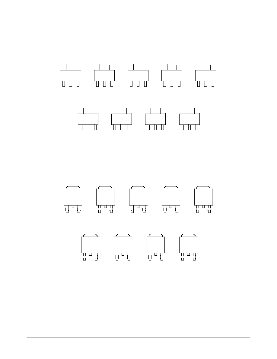
WW, W = Work Week
MARKING DIAGRAMS
DPAK
DT SUFFIX
CASE 369C
2
3
ALYW
17-15
1
2
3
ALYW
17-18
1
2
3
ALYW
117-2
1
2
3
ALYW
17-25
1
2
3
ALYW
7-285
1
2
3
ALYW
17-33
1
2
3
ALYW
117-5
1
2
3
ALYW
17-12
1
2
3
1
2
3
1
2
3
1
2
3
1
2
3
1
2
3
1
2
3
1
2
3
1
2
3
1
2
3
Adjustable
1.5 V
1.8 V
2.0 V
2.5 V
2.85 V
3.3 V
5.0 V
12 V
Adjustable
1.5 V
1.8 V
2.0 V
2.5 V
2.85 V
3.3 V
5.0 V
12 V

NCP1117, NCV1117
http://onsemi.com
14
PACKAGE DIMENSIONS
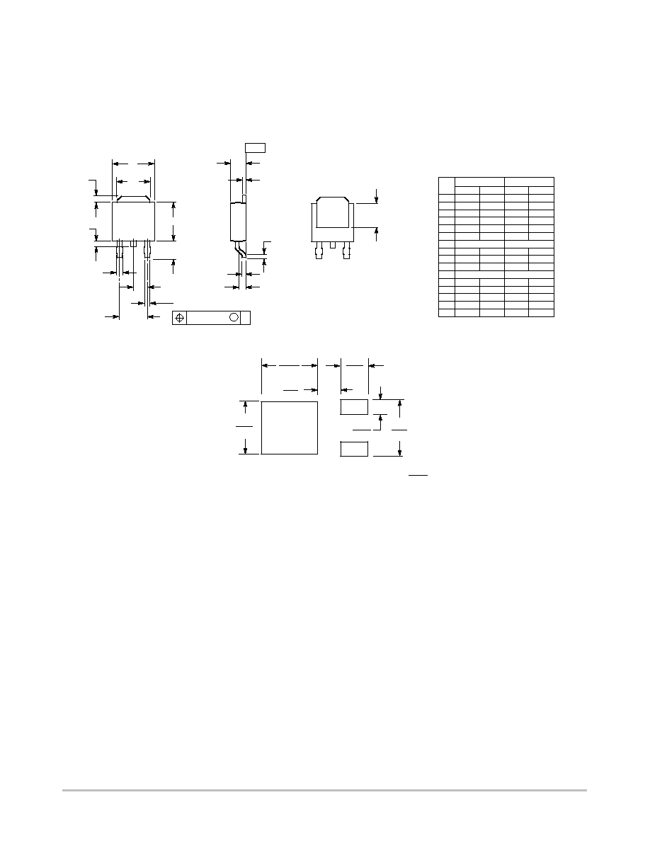
SOT-223
ST SUFFIX
CASE 318H-01
ISSUE O
……
……
NOTES:
1. DIMENSIONS ARE IN MILLIMETERS.
2. INTERPRET DIMENSIONS AND TOLERANCES
PER ASME Y14.5M, 1994.
3. DIMENSION E1 DOES NOT INCLUDE INTERLEAD
FLASH OR PROTRUSION. INTERLEAD FLASH OR
PROTRUSION SHALL NOT EXCEED 0.23 PER
SIDE.
4. DIMENSIONS b AND b2 DO NOT INCLUDE
DAMBAR PROTRUSION. ALLOWABLE DAMBAR
PROTRUSION SHALL BE 0.08 TOTAL IN EXCESS
OF THE b AND b2 DIMENSIONS AT MAXIMUM
MATERIAL CONDITION.
5. TERMINAL NUMBERS ARE SHOWN FOR
REFERENCE ONLY.
6. DIMENSIONS D AND E1 ARE TO BE DETERMINED
AT DATUM PLANE H.
DIM
MIN
MAX
MILLIMETERS
A
---
1.80
A1
0.02
0.11
b
0.60
0.88
b1
0.60
0.80
b2
2.90
3.10
b3
2.90
3.05
c
0.24
0.35
c1
0.24
0.30
D
6.30
6.70
E
6.70
7.30
E1
3.30
3.70
e
2.30
e1
4.60
L
0.25
---
T
0
10
T
_
_
c1
E
H
M
0.2
C
C
A
S
B
B
B
A
A
M
0.1
C
S
A
S
B
E1
B
D
4
3
2
1
e
e1
M
0.1
C
S
A
S
B
b2
b
A
0.08
A1
c
b1
(b)
(b2)
b3
SECTION B-B
L
««
…………………
…………………
««««««
SECTION A-A
1.5
0.059
mm
inches
SCALE 6:1
3.8
0.15
2.0
0.079
6.3
0.248
2.3
0.091
2.3
0.091
2.0
0.079
*For additional information on our Pb-Free strategy and soldering
details, please download the ON Semiconductor Soldering and
Mounting Techniques Reference Manual, SOLDERRM/D.
SOLDERING FOOTPRINT*
NCP1117, NCV1117
http://onsemi.com
15
PACKAGE DIMENSIONS
DPAK
DT SUFFIX
CASE 369C-01
ISSUE O
5.80
0.228
2.58
0.101
1.6
0.063
6.20
0.244
3.0
0.118
6.172
0.243
mm
inches
SCALE 3:1
*For additional information on our Pb-Free strategy and soldering
details, please download the ON Semiconductor Soldering and
Mounting Techniques Reference Manual, SOLDERRM/D.
SOLDERING FOOTPRINT*
D
A
K
B
R
V
S
F
L
G
2 PL
M
0.13 (0.005)
T
E
C
U
J
H
-T-
SEATING
PLANE
Z
DIM
MIN
MAX
MIN
MAX
MILLIMETERS
INCHES
A
0.235
0.245
5.97
6.22
B
0.250
0.265
6.35
6.73
C
0.086
0.094
2.19
2.38
D
0.027
0.035
0.69
0.88
E
0.018
0.023
0.46
0.58
F
0.037
0.045
0.94
1.14
G
0.180 BSC
4.58 BSC
H
0.034
0.040
0.87
1.01
J
0.018
0.023
0.46
0.58
K
0.102
0.114
2.60
2.89
L
0.090 BSC
2.29 BSC
R
0.180
0.215
4.57
5.45
S
0.025
0.040
0.63
1.01
U
0.020
---
0.51
---
V
0.035
0.050
0.89
1.27
Z
0.155
---
3.93
---
NOTES:
1. DIMENSIONING AND TOLERANCING
PER ANSI Y14.5M, 1982.
2. CONTROLLING DIMENSION: INCH.
1
2
3
4

NCP1117, NCV1117
http://onsemi.com
16
ON Semiconductor and are registered trademarks of Semiconductor Components Industries, LLC (SCILLC). SCILLC reserves the right to make changes without further notice
to any products herein. SCILLC makes no warranty, representation or guarantee regarding the suitability of its products for any particular purpose, nor does SCILLC assume any liability
arising out of the application or use of any product or circuit, and specifically disclaims any and all liability, including without limitation special, consequential or incidental damages.
"Typical" parameters which may be provided in SCILLC data sheets and/or specifications can and do vary in different applications and actual performance may vary over time. All
operating parameters, including "Typicals" must be validated for each customer application by customer's technical experts. SCILLC does not convey any license under its patent rights
nor the rights of others. SCILLC products are not designed, intended, or authorized for use as components in systems intended for surgical implant into the body, or other applications
intended to support or sustain life, or for any other application in which the failure of the SCILLC product could create a situation where personal injury or death may occur. Should
Buyer purchase or use SCILLC products for any such unintended or unauthorized application, Buyer shall indemnify and hold SCILLC and its officers, employees, subsidiaries, affiliates,
and distributors harmless against all claims, costs, damages, and expenses, and reasonable attorney fees arising out of, directly or indirectly, any claim of personal injury or death
associated with such unintended or unauthorized use, even if such claim alleges that SCILLC was negligent regarding the design or manufacture of the part. SCILLC is an Equal
Opportunity/Affirmative Action Employer. This literature is subject to all applicable copyright laws and is not for resale in any manner.
PUBLICATION ORDERING INFORMATION
N. American Technical Support: 800-282-9855 Toll Free
USA/Canada
Japan: ON Semiconductor, Japan Customer Focus Center
2-9-1 Kamimeguro, Meguro-ku, Tokyo, Japan 153-0051
Phone: 81-3-5773-3850
NCP1117/D
LITERATURE FULFILLMENT:
Literature Distribution Center for ON Semiconductor
P.O. Box 61312, Phoenix, Arizona 85082-1312 USA
Phone: 480-829-7710 or 800-344-3860 Toll Free USA/Canada
Fax: 480-829-7709 or 800-344-3867 Toll Free USA/Canada
Email: orderlit@onsemi.com
ON Semiconductor Website: http://onsemi.com
Order Literature: http://www.onsemi.com/litorder
For additional information, please contact your
local Sales Representative.