 | –≠–ª–µ–∫—Ç—Ä–æ–Ω–Ω—ã–π –∫–æ–º–ø–æ–Ω–µ–Ω—Ç: NCP1200A | –°–∫–∞—á–∞—Ç—å:  PDF PDF  ZIP ZIP |

©
Semiconductor Components Industries, LLC, 2004
October, 2004- Rev. 5
1
Publication Order Number:
NCP1200A/D
NCP1200A
PWM Current-Mode
Controller for Universal
Off-Line Supplies Featuring
Low Standby Power
Housed in SOIC-8 or PDIP-8 package, the NCP1200A enhances
the previous NCP1200 series by offering a reduced optocoupler
current together with an increased drive capability. Due to its novel
concept, the circuit allows the implementation of complete off-line
AC-DC adapters, battery charger or a SMPS where standby power is a
key parameter.
With an internal structure operating at a fixed 40 kHz, 60 kHz or
100 kHz, the controller supplies itself from the high-voltage rail,
avoiding the need of an auxiliary winding. This feature naturally eases
the designer task in battery charger applications. Finally,
current-mode control provides an excellent audio-susceptibility and
inherent pulse-by-pulse control.
When the current setpoint falls below a given value, e.g. the output
power demand diminishes, the IC automatically enters the so-called
skip cycle mode and provides excellent efficiency at light loads.
Because this occurs at a user adjustable low peak current, no acoustic
noise takes place.
The NCP1200A features an efficient protective circuitry which, in
presence of an overcurrent condition, disables the output pulses while
the device enters a safe burst mode, trying to restart. Once the default
has gone, the device auto-recovers.
Features
∑
Pb-Free Packages are Available
∑
No Auxiliary Winding Operation
∑
Auto-Recovery Internal Output Short-Circuit Protection
∑
Extremely Low No-Load Standby Power
∑
Current-Mode Control with Skip-Cycle Capability
∑
Internal Temperature Shutdown
∑
Internal Leading Edge Blanking
∑
250 mA Peak Current Capability
∑
Internally Fixed Frequency at 40 kHz, 60 kHz and 100 kHz
∑
Direct Optocoupler Connection
∑
SPICE Models Available for TRANsient and AC Analysis
∑
Pin to Pin Compatible with NCP1200
Typical Applications
∑
AC-DC Adapters for Portable Devices
∑
Offline Battery Chargers
∑
Auxiliary Power Supplies (USB, Appliances, TVs, etc.)
SOIC-8
D SUFFIX
CASE 751
1
8
MARKING
DIAGRAMS
PIN CONNECTIONS
PDIP-8
P SUFFIX
CASE 626
1
8
1
8
1200APxxx
AWL
YYWW
200Ay
ALYW
xxx
= Specific Device Code
(40, 60 or 100)
y
= Specific Device Code
(4 for 40, 6 for 60, 1 for 100)
A
= Assembly Location
WL, L
= Wafer Lot
Y, YY
= Year
W, WW = Work Week
1
Adj
8 HV
2
FB
3
CS
4
GND
7 NC
6 V
CC
5 Drv
(Top View)
MINIATURE PWM
CONTROLLER FOR HIGH
POWER AC-DC WALL
ADAPTERS AND OFFLINE
BATTERY CHARGERS
See detailed ordering and shipping information in the package
dimensions section on page 13 of this data sheet.
ORDERING INFORMATION
http://onsemi.com
1
8

NCP1200A
http://onsemi.com
2
Figure 1. Typical Application Example
EMI
FILTER
UNIVERSAL
INPUT
+
+
NCP1200A
+
V
OUT
Adj
FB
CS
GND
HV
V
CC
Drv
1
2
3
4
8
7
6
5
*
*Please refer to the application information section
PIN FUNCTION DESCRIPTION
Pin No.
Pin Name
Function
Pin Description
1
Adj
Adjust the skipping peak current
This pin lets you adjust the level at which the cycle skipping process takes
place. Shorting this pin to ground, permanently disables the skip cycle
feature.
2
FB
Sets the peak current setpoint
By connecting an optocoupler to this pin, the peak current setpoint is
adjusted accordingly to the output power demand.
3
CS
Current sense input
This pin senses the primary current and routes it to the internal comparator
via an L.E.B.
4
GND
The IC ground
-
5
Drv
Driving pulses
The driver's output to an external MOSFET.
6
V
CC
Supplies the IC
This pin is connected to an external bulk capacitor of typically 10
m
F.
7
NC
-
This unconnected pin ensures adequate creepage distance.
8
HV
Generates the V
CC
from the line
Connected to the high-voltage rail, this pin injects a constant current into
the V
CC
bulk capacitor.

NCP1200A
http://onsemi.com
3
Figure 2. Internal Circuit Architecture
OVERLOAD?
UVLO HIGH AND LOW
INTERNAL REGULATOR
±
250 mA
HV CURRENT
SOURCE
INTERNAL V
CC
8
7
6
5
HV
NC
V
CC
Drv
1
2
3
4
Q FLIP-FLOP
DCmax = 80%
Q
250 ns
L.E.B.
40-60-100 kHz
CLOCK
-
+
-
+
80 k
20 k
57 k
1 V
CURRENT
SENSE
GROUND
FB
Adj
24 k
25 k
+
-
V
REF
RESET
1.2 V
SKIP CYCLE
COMPARATOR
SET
FAULT DURATION
5 V
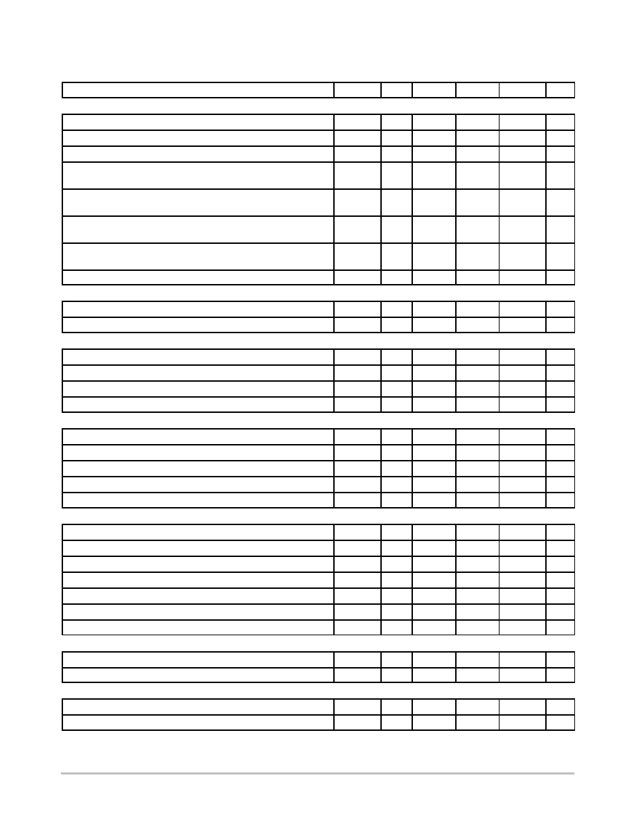
MAXIMUM RATINGS
Rating
Symbol
Value
Unit
Power Supply Voltage
V
CC
16
V
Thermal Resistance Junction-to-Air, PDIP-8 Version
Thermal Resistance Junction-to-Air, SOIC Version
R
q
JA
R
q
JA
100
178
∞
C/W
∞
C/W
Maximum Junction Temperature
T
J(max)
150
∞
C
Temperature Shutdown
-
145
∞
C
Storage Temperature Range
-
-60 to +150
∞
C
ESD Capability, HBM Model (All pins except V
CC
and HV)
-
2.0
kV
ESD Capability, Machine Model
-
200
V
Maximum Voltage on Pin 8 (HV), Pin 6 (V
CC
) Grounded
-
450
V
Maximum Voltage on Pin 8 (HV), Pin 6 (V
CC
) Decoupled to Ground with 10
m
F
-
500
V
Minimum Operating Voltage on Pin 8 (HV)
-
40
V
Maximum ratings are those values beyond which device damage can occur. Maximum ratings applied to the device are individual stress limit
values (not normal operating conditions) and are not valid simultaneously. If these limits are exceeded, device functional operation is not implied,
damage may occur and reliability may be affected.
NCP1200A
http://onsemi.com
4
ELECTRICAL CHARACTERISTICS
(For typical values T
J
= 25
∞
C, for min/max values T
J
= 0
∞
C to +125
∞
C, Max T
J
= 150
∞
C,
V
CC
= 11 V unless otherwise noted.)
Characteristic
Symbol
Pin
Min
Typ
Max
Unit
Dynamic Self-Supply (All frequency versions, otherwise noted)
V
CC
Increasing Level at which the Current Source Turns-Off
V
CC(off)
6
11.2
12.1
13.1
V
V
CC
Decreasing Level at which the Current Source Turns-On
V
CC(on)
6
9.0
10
11
V
V
CC
Decreasing Level at which the Latchoff Phase Ends
V
CC(latch)
6
-
5.4
-
V
Internal IC Consumption, No Output Load on Pin 5
ICC1
6
-
750
1000
(Note 1)
m
A
Internal IC Consumption, 1.0 nF Output Load on Pin 5, F
SW
= 40 kHz
ICC2
6
-
1.2
1.4
(Note 2)
mA
Internal IC Consumption, 1.0 nF Output Load on Pin 5, F
SW
= 60 kHz
ICC2
6
-
1.4
1.6
(Note 2)
mA
Internal IC Consumption, 1.0 nF Output Load on Pin 5, F
SW
= 100 kHz
ICC2
6
-
1.9
2.2
(Note 2)
mA
Internal IC Consumption, Latchoff Phase
ICC3
6
-
350
-
m
A
Internal Startup Current Source
(T
J
> 0
∞
C, pin 8 biased at 50 V)
High-Voltage Current Source, V
CC
= 10 V
IC1
8
4.0
7.0
-
mA
High-Voltage Current Source, V
CC
= 0
IC2
8
-
13
-
mA
Drive Output
Output Voltage Rise-Time @ CL = 1.0 nF, 10-90% of Output Signal
T
r
5
-
67
-
ns
Output Voltage Fall-Time @ CL = 1.0 nF, 10-90% of Output Signal
T
f
5
-
25
-
ns
Source Resistance
R
OH
5
27
40
61
W
Sink Resistance
R
OL
5
5.0
10
21
W
Current Comparator (Pin 5 unloaded unless otherwise noted)
Input Bias Current @ 1.0 V Input Level on Pin 3
I
IB
3
-
0.02
-
m
A
Maximum Internal Current Setpoint (Note 3)
I
Limit
3
0.8
0.9
1.0
V
Default Internal Current Setpoint for Skip Cycle Operation
I
Lskip
3
-
360
-
mV
Propagation Delay from Current Detection to Gate OFF State
T
DEL
3
-
90
160
ns
Leading Edge Blanking Duration (Note 3)
T
LEB
3
-
250
-
ns
Internal Oscillator (V
CC
= 11 V, pin 5 loaded by 1.0 k
W
)
Oscillation Frequency, 40 kHz Version
f
OSC
-
37
43
48
kHz
Built-in Frequency Jittering, f
sw
= 40 kHz
f
jitter
-
-
350
-
kHz
Oscillation Frequency, 60 kHz Version
f
OSC
-
53
61
68
kHz
Built-in Frequency Jittering, f
sw
= 60 kHz
f
jitter
-
-
460
-
kHz
Oscillation Frequency, 100 kHz Version
f
OSC
-
90
103
114
kHz
Built-in Frequency Jittering, f
sw
= 100 kHz
f
jitter
-
-
620
-
kHz
Maximum Duty Cycle
Dmax
-
74
83
87
%
Feedback Section (V
CC
= 11 V, pin 5 unloaded)
Internal Pullup Resistor
R
up
2
-
20
-
k
W
Pin 3 to Current Setpoint Division Ratio
I
ratio
-
-
3.3
-
-
Skip Cycle Generation
Default Skip Mode Level
V
skip
1
0.95
1.2
1.45
V
Pin 1 Internal Output Impedance
Z
out
1
-
22
-
k
W
1. Max value at T
J
= 0
∞
C.
2. Maximum value @ T
J
= 25
∞
C, please see characterization curves.
3. Pin 5 loaded by 1.0 nF.
NCP1200A
http://onsemi.com
5
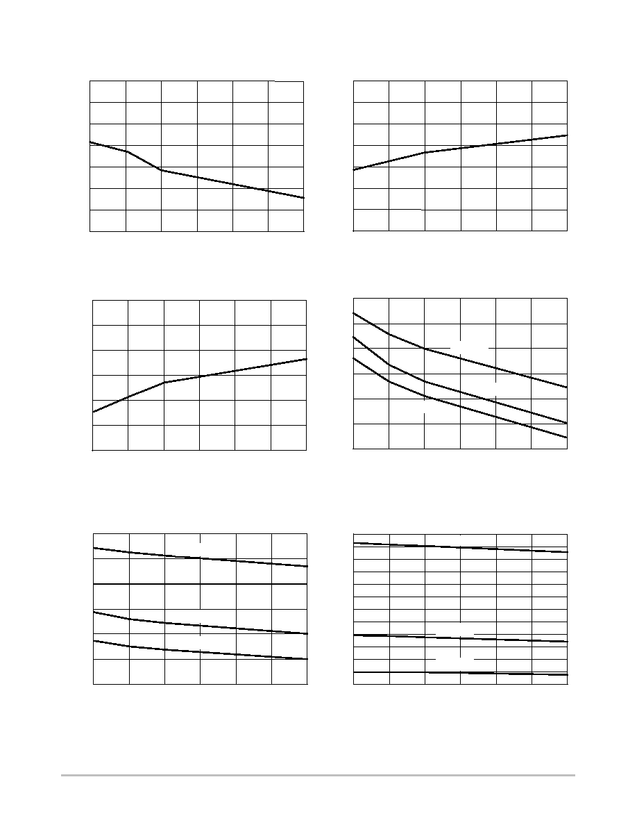
TYPICAL CHARACTERISTICS
9.6
9.7
9.8
9.9
10.0
10.1
10.2
-25
0
25
50
75
100
125
600
650
700
750
800
850
900
-25
0
25
50
75
100
125
0
10
20
30
40
50
60
70
-25
0
25
50
75
100
125
11.1
11.3
11.5
11.7
11.9
12.1
12.3
12.5
-25
0
25
50
75
100
125
0.90
1.10
1.30
1.50
1.70
1.90
2.10
-25
0
25
50
75
100
125
38
44
50
56
62
68
74
80
86
92
98
104
110
-25
0
25
50
75
100
125
TEMPERATURE (
∞
C)
LEAKAGE (
m
A)
Figure 3. HV Pin Leakage Current vs. Temperature
TEMPERATURE (
∞
C)
V
CC(of
f)
, THRESHOLD (V)
Figure 4. V
CC(off)
vs. Temperature
TEMPERATURE (
∞
C)
V
CC(on)
, (V)
Figure 5. V
CC(on)
vs. Temperature
TEMPERATURE (
∞
C)
ICC1 (
m
A)
100 kHz
60 kHz
40 kHz
Figure 6. ICC1 vs. Temperature
TEMPERATURE (
∞
C)
ICC2 (mA)
100 kHz
60 kHz
40 kHz
Figure 7. ICC2 vs. Temperature
TEMPERATURE (
∞
C)
F
SW
(kHz)
100 kHz
60 kHz
40 kHz
Figure 8. Switching Frequency vs. Temperature

NCP1200A
http://onsemi.com
6
TYPICAL CHARACTERISTICS
1.00
1.05
1.10
1.15
1.20
1.25
1.30
1.35
1.40
-25
0
25
50
75
100
125
-25
0
25
50
75
100
125
TEMPERATURE (
∞
C)
ICC3 (
m
A)
190
220
250
280
310
340
370
400
430
460
490
Figure 9. V
CC
Latchoff vs. Temperature
Figure 10. ICC3 vs. Temperature
Figure 11. Drive and Source Resistance vs.
Temperature
TEMPERATURE (
∞
C)
CURRENT SETPOINT (V)
Figure 12. Current Sense Limit vs. Temperature
TEMPERATURE (
∞
C)
V
SKIP
(V)
Figure 13. V
SKIP
vs. Temperature
Figure 14. Max Duty Cycle vs. Temperature
TEMPERATURE (
∞
C)
V
CC
LA
TCHOFF
5.15
5.20
5.25
5.30
5.35
5.40
5.45
5.50
-25
0
25
50
75
100
125
TEMPERATURE (
∞
C)
DUTY MAX (%)
-25
0
25
50
75
100
125
TEMPERATURE (
∞
C)
Ohm
0
10
20
30
40
50
60
Sink
Source
0.80
0.84
0.88
0.92
0.96
1.00
-25
0
25
50
75
100
125
73
75
77
79
81
83
85
87
-25
0
25
50
75
100
125
NCP1200A
http://onsemi.com
7
APPLICATION INFORMATION
Introduction
The NCP1200A implements a standard current mode
architecture where the switch-off time is dictated by the
peak current setpoint. This component represents the ideal
candidate where low part-count is the key parameter,
particularly in low-cost AC-DC adapters, auxiliary
supplies, etc. Due to its high-performance High-Voltage
technology, the NCP1200A incorporates all the necessary
components normally needed in UC384X based supplies:
timing components, feedback devices, low-pass filter and
self-supply. This later point emphasizes the fact that
ON Semiconductor's NCP1200A does NOT need an
auxiliary winding to operate: the product is naturally
supplied from the high-voltage rail and delivers a V
CC
to the
IC. This system is called the Dynamic Self-Supply (DSS).
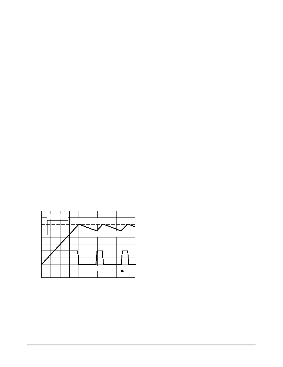
Dynamic Self-Supply
The DSS principle is based on the charge/discharge of the
V
CC
bulk capacitor from a low level up to a higher level. We
can easily describe the current source operation with a bunch
of simple logical equations:
POWER-ON: IF V
CC
< VCC
H
THEN Current Source is
ON, no output pulses
IF V
CC
decreasing > VCC
L
THEN Current Source is OFF,
output is pulsing
IF V
CC
increasing < VCC
H
THEN Current Source is ON,
output is pulsing
Typical values are: VCC
H
= 12 V, VCC
L
= 10 V
To better understand the operational principle, Figure 15's
sketch offers the necessary light:
Figure 15. The charge/discharge cycle over a
10
m
F V
CC
capacitor
10.0 M
30.0 M
50.0 M
70.0 M
90.0 M
V
CC
Current
Source
OFF
ON
OUTPUT PULSES
V
ripple
= 2 V
UVLO
H
= 12 V
UVLO
L
= 10 V
The DSS behavior actually depends on the internal IC
consumption and the MOSFET's gate charge Qg. If we
select a MOSFET like the MTP2N60E, Qg max equals
22 nC. With a maximum switching frequency of 68 kHz for
the P60 version, the average power necessary to drive the
MOSFET (excluding the driver efficiency and neglecting
various voltage drops) is:
F
SW
Qg
V
CC
with
F
SW
= maximum switching frequency
Qg = MOSFET's gate charge
V
CC
= V
GS
level applied to the gate
To obtain the final IC current, simply divide this result by
V
CC
: I
driver
= F
SW
Qg = 1.5 mA. The total standby power
consumption at no-load will therefore heavily rely on the
internal IC consumption plus the above driving current
(altered by the driver's efficiency). Suppose that the IC is
supplied from a 350 VDC line. The current flowing through
pin 8 is a direct image of the NCP1200A consumption
(neglecting the switching losses of the HV current source).
If ICC2 equals 2.3 mA @ T
J
= 25
∞
C, then the power
dissipated (lost) by the IC is simply: 350 x 2.3 m = 805 mW.
For design and reliability reasons, it would be interesting to
reduce this source of wasted power which increases the die
temperature. This can be achieved by using different
methods:
1. Use a MOSFET with lower gate charge Qg
2. Connect pin through a diode (1N4007 typically) to
one of the mains input. The average value on pin 8
becomes
VMAINS(peak)
@
2
p
. Our power
contribution example drops to: 223 x 2.3 m = 512
mW. If a resistor is installed between the mains and
the diode, you further force the dissipation to
migrate from the package to the resistor. The
resistor value should account for low-line startups.
3. Permanently force the V
CC
level above VCC
H
with
an auxiliary winding. It will automatically
disconnect the internal startup source and the IC
will be fully self-supplied from this winding.
Again, the total power drawn from the mains will
significantly decrease. Make sure the auxiliary
voltage never exceeds the 16 V limit.

NCP1200A
http://onsemi.com
8
Figure 16. A simple diode naturally reduces the average voltage on pin 8
8
7
6
5
1
2
3
4
mains
Cbulk
HV
Skipping Cycle Mode
The NCP1200A automatically skips switching cycles
when the output power demand drops below a given level.
This is accomplished by monitoring the FB pin. In normal
operation, pin 2 imposes a peak current accordingly to the
load value. If the load demand decreases, the internal loop
asks for less peak current. When this setpoint reaches a
determined level, the IC prevents the current from
decreasing further down and starts to blank the output
pulses: the IC enters the so-called skip cycle mode, also
named controlled burst operation. The power transfer now
depends upon the width of the pulse bunches (Figure 18).
Suppose we have the following component values:
Lp, primary inductance = 1 mH
F
SW
, switching frequency = 61 kHz
Ip skip = 200 mA (or 333 mV/R
SENSE
)
The theoretical power transfer is therefore:
1
2
@
Lp
@
Ip
2
@
FSW
+
1.2 W
If this IC enters skip cycle mode with a bunch length of
20 ms over a recurrent period of 100 ms, then the total
power transfer is: 1.2 . 0.2 = 240 mW.
To better understand how this skip cycle mode takes place,
a look at the operation mode versus the FB level
immediately gives the necessary insight:
Figure 17.
SKIP CYCLE OPERATION
I
P(min)
= 333 mV/R
SENSE
NORMAL CURRENT
MODE OPERATION
FB
1 V
4.2 V, FB Pin Open
3.2 V, Upper
Dynamic Range
When FB is above the skip cycle threshold (1 V by
default), the peak current cannot exceed 1 V/R
SENSE
. When
the IC enters the skip cycle mode, the peak current cannot go
below Vpin1 / 3.3. The user still has the flexibility to alter
this 1 V by either shunting pin 1 to ground through a resistor
or raising it through a resistor up to the desired level.
Grounding pin 1 permanently invalidates the skip cycle
operation.
Power P1
Power P2
Power P3
Figure 18. Output Pulses at Various Power Levels (X = 5.0
m
s/div) P1
t
P2
t
P3
NCP1200A
http://onsemi.com
9
Figure 19. The Skip Cycle Takes Place at Low Peak Currents which Guaranties Noise-Free
Operation
315.40
882.70
1.450 M
2.017 M
2.585 M
300 M
200 M
100 M
0
MAX PEAK
CURRENT
SKIP CYCLE
CURRENT LIMIT
We recommend a pin 1 operation between 400 mV and 1.3
V that will fix the skip peak current level between 120 mV
/ RSENSE and 390 mV / RSENSE.
Non-Latching Shutdown
In some cases, it might be desirable to shut off the part
temporarily and authorize its restart once the default has
disappeared. This option can easily be accomplished
through a single NPN bipolar transistor wired between FB
and ground. By pulling FB below the Adj pin 1 level, the
output pulses are disabled as long as FB is pulled below
pin 1. As soon as FB is relaxed, the IC resumes its operation.
Figure 20 depicts the application example:
Figure 20. Another Way of Shutting Down the IC without a Definitive Latchoff State
ON/OFF
Q1
8
7
6
5
1
2
3
4

NCP1200A
http://onsemi.com
10
Power Dissipation
The NCP1200A is directly supplied from the DC rail
through the internal DSS circuitry. The average current
flowing through the DSS is therefore the direct image of the
NCP1200A current consumption. The total power
dissipation can be evaluated using: (V
HVDC
- 11 V)
ICC2.
If we operate the device on a 250 VAC rail, the maximum
rectified voltage can go up to 350 VDC. However, as the
characterization curves show, the current consumption
drops at high junction temperature, which quickly occurs
due to the DSS operation. At T
J
= 50
∞
C, ICC2 = 1.7 mA for
the 61 kHz version over a 1 nF capacitive load. As a result,
the NCP1200A will dissipate 350 . 1.7 mA@T
J
= 50
∞
C =
595 mW. The SOIC-8 package offers a
junction-to-ambient thermal resistance R
qJA
of 178
∞
C/W.
Adding some copper area around the PCB footprint will help
decreasing this number: 12 mm x 12 mm to drop R
qJA
down
to 100
∞
C/W with 35
m copper thickness (1 oz.) or 6.5 mm x
6.5 mm with 70
m copper thickness (2 oz.). With this later
number, we can compute the maximum power dissipation
the package accepts at an ambient of 50
∞
C:
Pmax
+
TJmax
*
TAmax
R
q
JA
+
750 mW
which is okay with
our previous budget. For the DIP8 package, adding a
min-pad area of 80 mm
@ of 35 m copper (1 oz.), R
qJA
drops
from 100
∞
C/W to about 75
∞
C/W.
In the above calculations, ICC2 is based on a 1 nF output
capacitor. As seen before, ICC2 will depend on your
MOSFET's Qg: ICC2
ICC1 + F
SW
x Qg. Final calculation
shall thus accounts for the total gate-charge Qg your
MOSFET will exhibit. The same methodology can be
applied for the 100 kHz version but care must be taken to
keep T
J
below the 125
∞
C limit with the D100 (SOIC) version
and activated DSS in high-line conditions.
If the power estimation is beyond the limit, other solutions
are possible a) add a series diode with pin 8 (as suggested in
the above lines) and connect it to the half rectified wave. As
a result, it will drop the average input voltage and lower the
dissipation to:
350
@
2
p
@
1.7 m
+
380 mW
b) put an
auxiliary
winding to disable the DSS and decrease the power
consumption to V
CC
x ICC2. The auxiliary level should be
thus that the rectified auxiliary voltage permanently stays
above 10 V (to not re-activate the DSS) and is safely kept
below the 16 V maximum rating.
Overload Operation
In applications where the output current is purposely not
controlled (e.g. wall adapters delivering raw DC level), it is
interesting to implement a true short-circuit protection. A
short-circuit actually forces the output voltage to be at a low
level, preventing a bias current to circulate in the
optocoupler LED. As a result, the FB pin level is pulled up
to 4.2 V, as internally imposed by the IC. The peak current
setpoint goes to the maximum and the supply delivers a
rather high power with all the associated effects. Please note
that this can also happen in case of feedback loss, e.g. a
broken optocoupler. To account for this situation,
NCP1200A hosts a dedicated overload detection circuitry.
Once activated, this circuitry imposes to deliver pulses in a
burst manner with a low duty cycle. The system
auto-recovers when the fault condition disappears.
During the startup phase, the peak current is pushed to the
maximum until the output voltage reaches its target and the
feedback loop takes over. This period of time depends on
normal output load conditions and the maximum peak
current allowed by the system. The time-out used by this IC
works with the V
CC
decoupling capacitor: as soon as the
V
CC
decreases from the UVLO
H
level (typically 12 V) the
device internally watches for an overload current situation.
If this condition is still present when the UVLO
L
level is
reached, the controller stops the driving pulses, prevents the
self-supply current source to restart and puts all the circuitry
in standby, consuming as little as 350
mA typical (ICC3
parameter). As a result, the V
CC
level slowly discharges
toward 0.

NCP1200A
http://onsemi.com
11
DRIVER
PULSES
DRIVER
PULSES
TIME
TIME
TIME
Drv
V
CC
12 V
10 V
5.4 V
REGULATION
OCCURS
HERE
INTERNAL
FAULT FLAG
FAULT IS
RELAXED
FAULT OCCURS HERE
LATCHOFF
PHASE
STARTUP PHASE
Figure 21. If the fault is relaxed during the V
CC
natural fall down sequence, the IC automatically resumes.
If the fault still persists when V
CC
reached UVLO
L
, then the controller cuts everything off until recovery.
When this level crosses 5.4 V typical, the controller enters
a new startup phase by turning the current source on: V
CC
rises toward 12 V and again delivers output pulses at the
UVLO
H
crossing point. If the fault condition has been
removed before UVLO
L
approaches, then the IC continues
its normal operation. Otherwise, a new fault cycle takes
place. Figure 21 shows the evolution of the signals in
presence of a fault.
Calculating the V
CC
Capacitor
As the above section describes, the fall down sequence
depends upon the V
CC
level: how long does it take for the
V
CC
line to go from 12 V to 10 V? The required time depends
on the startup sequence of your system, i.e. when you first
apply the power to the IC. The corresponding transient fault
duration due to the output capacitor charging must be less
than the time needed to discharge from 12 V to 10 V,
otherwise the supply will not properly start. The test consists
in either simulating or measuring in the lab how much time
the system takes to reach the regulation at full load. Let's
suppose that this time corresponds to 6 ms. Therefore a V
CC
fall time of 10 ms could be well appropriated in order to not
trigger the overload detection circuitry. If the corresponding
IC consumption, including the MOSFET drive, establishes
at 1.8 mA for instance, we can calculate the required
capacitor using the following formula:
D
t
+ D
V
@
C
i
, with
DV = 2 V. Then for a wanted Dt of 10 ms, C equals 9 mF or
22
mF for a standard value. When an overload condition
occurs, the IC blocks its internal circuitry and its
consumption drops to 350
mA typical. This happens at
V
CC
= 10 V and it remains stuck until V
CC
reaches 5.4 V: we
are in latchoff phase. Again, using the calculated 22
mF and
350
mA current consumption, this latchoff phase lasts:
296 ms.

NCP1200A
http://onsemi.com
12
Protecting the Controller Against Negative Spikes
As with any controller built upon a CMOS technology, it
is the designer's duty to avoid the presence of negative
spikes on sensitive pins. Negative signals have the bad habit
to forward bias the controller substrate and induce erratic
behaviors. Sometimes, the injection can be so strong that
internal parasitic SCRs are triggered, engendering
irremediable damages to the IC if they are a low impedance
path is offered between V
CC
and GND. If the current sense
pin is often the seat of such spurious signals, the
high-voltage pin can also be the source of problems in
certain circumstances. During the turn-off sequence, e.g.
when the user unplugs the power supply, the controller is still
fed by its V
CC
capacitor and keeps activating the MOSFET
ON and OFF with a peak current limited by Rsense.
Unfortunately, if the quality coefficient Q of the resonating
network formed by Lp and Cbulk is low (e.g. the MOSFET
Rdson + Rsense are small), conditions are met to make the
circuit resonate and thus negatively bias the controller. Since
we are talking about ms pulses, the amount of injected
charge (Q = I x t) immediately latches the controller which
brutally discharges its V
CC
capacitor. If this V
CC
capacitor
is of sufficient value, its stored energy damages the
controller. Figure 22 depicts a typical negative shot
occurring on the HV pin where the brutal V
CC
discharge
testifies for latchup.
Figure 22. A negative spike takes place on the Bulk capacitor at the switch-off sequence
Simple and inexpensive cures exist to prevent from
internal parasitic SCR activation. One of them consists in
inserting a resistor in series with the high-voltage pin to
keep the negative current to the lowest when the bulk
becomes negative (Figure 23). Please note that the negative
spike is clamped to ≠2 x Vf due to the diode bridge. Please
refer to AND8069/D for power dissipation calculations.
Another option (Figure 24) consists in wiring a diode from
V
CC
to the bulk capacitor to force V
CC
to reach UVLOlow
sooner and thus stops the switching activity before the bulk
capacitor gets deeply discharged. For security reasons, two
diodes can be connected in series.
Figure 23. A simple resistor in series avoids any
latchup in the controller
CV
CC
D3
1N4007
8
7
6
5
1
2
3
4
+
Cbulk
+
1
3
CV
CC
Rbulk
> 4.7 k
8
7
6
5
1
2
3
4
+
Cbulk
+
1
2
3
Figure 24. or a diode forces V
CC
to reach
UVLOlow sooner

NCP1200A
http://onsemi.com
13
ORDERING INFORMATION
Device
Type
Marking
Package
Shipping
NCP1200AP40
1200AP40
PDIP-8
50 Units / Rail
NCP1200AP40G
F
SW
= 40 kHz
1200AP40
PDIP-8
(Pb-Free)
50 Units / Rail
NCP1200AD40R2
200A4
SOIC-8
2500 Units /Reel
NCP1200AP60
1200AP60
PDIP-8
50 Units / Rail
NCP1200AP60G
F
= 60 kHz
1200AP60
PDIP-8
(Pb-Free)
50 Units / Rail
NCP1200AD60R2
F
SW
= 60 kHz
200A6
SOIC-8
2500 Units /Reel
NCP1200AD60R2G
200A6
SOIC-8
(Pb-Free)
2500 Units /Reel
NCP1200AP100
1200AP100
PDIP-8
50 Units / Rail
NCP1200AP100G
F
= 100 kHz
1200AP100
PDIP-8
(Pb-Free)
50 Units / Rail
NCP1200AD100R2
F
SW
= 100 kHz
200A1
SOIC-8
2500 Units / Reel
NCP1200AD100R2G
200A1
SOIC-8
(Pb-Free)
2500 Units / Reel
For information on tape and reel specifications, including part orientation and tape sizes, please refer to our Tape and Reel Packaging
Specifications Brochure, BRD8011/D.

NCP1200A
http://onsemi.com
14
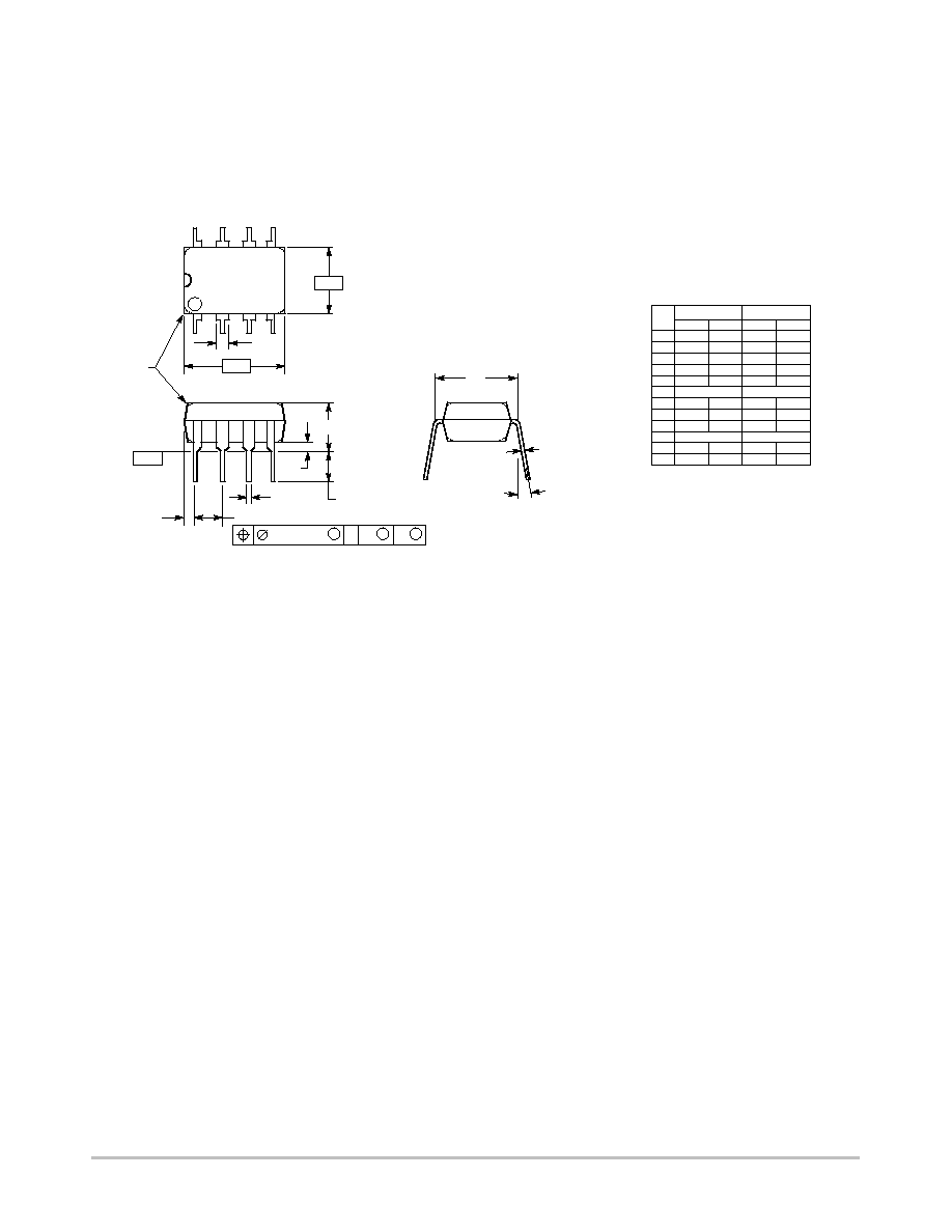
PACKAGE DIMENSIONS
SOIC-8
D SUFFIX
CASE 751-07
ISSUE AC
*For additional information on our Pb-Free strategy and soldering
details, please download the ON Semiconductor Soldering and
Mounting Techniques Reference Manual, SOLDERRM/D.
SOLDERING FOOTPRINT*
SEATING
PLANE
1
4
5
8
N
J
X 45
_
K
NOTES:
1. DIMENSIONING AND TOLERANCING PER
ANSI Y14.5M, 1982.
2. CONTROLLING DIMENSION: MILLIMETER.
3. DIMENSION A AND B DO NOT INCLUDE
MOLD PROTRUSION.
4. MAXIMUM MOLD PROTRUSION 0.15 (0.006)
PER SIDE.
5. DIMENSION D DOES NOT INCLUDE DAMBAR
PROTRUSION. ALLOWABLE DAMBAR
PROTRUSION SHALL BE 0.127 (0.005) TOTAL
IN EXCESS OF THE D DIMENSION AT
MAXIMUM MATERIAL CONDITION.
6. 751-01 THRU 751-06 ARE OBSOLETE. NEW
STANDARD IS 751-07.
A
B
S
D
H
C
0.10 (0.004)
DIM
A
MIN
MAX
MIN
MAX
INCHES
4.80
5.00
0.189
0.197
MILLIMETERS
B
3.80
4.00
0.150
0.157
C
1.35
1.75
0.053
0.069
D
0.33
0.51
0.013
0.020
G
1.27 BSC
0.050 BSC
H
0.10
0.25
0.004
0.010
J
0.19
0.25
0.007
0.010
K
0.40
1.27
0.016
0.050
M
0
8
0
8
N
0.25
0.50
0.010
0.020
S
5.80
6.20
0.228
0.244
-X-
-Y-
G
M
Y
M
0.25 (0.010)
-Z-
Y
M
0.25 (0.010)
Z
S
X
S
M
_
_
_
_
1.52
0.060
7.0
0.275
0.6
0.024
1.270
0.050
4.0
0.155
mm
inches
SCALE 6:1
NCP1200A
http://onsemi.com
15
PACKAGE DIMENSIONS
PDIP-8
P SUFFIX
CASE 626-05
ISSUE L
NOTES:
1. DIMENSION L TO CENTER OF LEAD WHEN
FORMED PARALLEL.
2. PACKAGE CONTOUR OPTIONAL (ROUND OR
SQUARE CORNERS).
3. DIMENSIONING AND TOLERANCING PER ANSI
Y14.5M, 1982.
1
4
5
8
F
NOTE 2
-A-
-B-
-T-
SEATING
PLANE
H
J
G
D
K
N
C
L
M
M
A
M
0.13 (0.005)
B
M
T
DIM
MIN
MAX
MIN
MAX
INCHES
MILLIMETERS
A
9.40
10.16
0.370
0.400
B
6.10
6.60
0.240
0.260
C
3.94
4.45
0.155
0.175
D
0.38
0.51
0.015
0.020
F
1.02
1.78
0.040
0.070
G
2.54 BSC
0.100 BSC
H
0.76
1.27
0.030
0.050
J
0.20
0.30
0.008
0.012
K
2.92
3.43
0.115
0.135
L
7.62 BSC
0.300 BSC
M
---
10
---
10
N
0.76
1.01
0.030
0.040
_
_

NCP1200A
http://onsemi.com
16
ON Semiconductor and are registered trademarks of Semiconductor Components Industries, LLC (SCILLC). SCILLC reserves the right to make changes without further notice
to any products herein. SCILLC makes no warranty, representation or guarantee regarding the suitability of its products for any particular purpose, nor does SCILLC assume any liability
arising out of the application or use of any product or circuit, and specifically disclaims any and all liability, including without limitation special, consequential or incidental damages.
"Typical" parameters which may be provided in SCILLC data sheets and/or specifications can and do vary in different applications and actual performance may vary over time. All
operating parameters, including "Typicals" must be validated for each customer application by customer's technical experts. SCILLC does not convey any license under its patent rights
nor the rights of others. SCILLC products are not designed, intended, or authorized for use as components in systems intended for surgical implant into the body, or other applications
intended to support or sustain life, or for any other application in which the failure of the SCILLC product could create a situation where personal injury or death may occur. Should
Buyer purchase or use SCILLC products for any such unintended or unauthorized application, Buyer shall indemnify and hold SCILLC and its officers, employees, subsidiaries, affiliates,
and distributors harmless against all claims, costs, damages, and expenses, and reasonable attorney fees arising out of, directly or indirectly, any claim of personal injury or death
associated with such unintended or unauthorized use, even if such claim alleges that SCILLC was negligent regarding the design or manufacture of the part. SCILLC is an Equal
Opportunity/Affirmative Action Employer. This literature is subject to all applicable copyright laws and is not for resale in any manner.
PUBLICATION ORDERING INFORMATION
N. American Technical Support: 800-282-9855 Toll Free
USA/Canada
Japan: ON Semiconductor, Japan Customer Focus Center
2-9-1 Kamimeguro, Meguro-ku, Tokyo, Japan 153-0051
Phone: 81-3-5773-3850
NCP1200A/D
The product described herein (NCP1200A), may be covered by the following U.S. patents: 6,271,735, 6,362,067, 6,385,060, 6,429,709, 6,587,357. There
may be other patents pending.
LITERATURE FULFILLMENT:
Literature Distribution Center for ON Semiconductor
P.O. Box 61312, Phoenix, Arizona 85082-1312 USA
Phone: 480-829-7710 or 800-344-3860 Toll Free USA/Canada
Fax: 480-829-7709 or 800-344-3867 Toll Free USA/Canada
Email: orderlit@onsemi.com
ON Semiconductor Website: http://onsemi.com
Order Literature: http://www.onsemi.com/litorder
For additional information, please contact your
local Sales Representative.