©
Semiconductor Components Industries, LLC, 2004
December, 2004 - Rev. 13
1
Publication Order Number:
NCP1200/D
NCP1200
PWM Current-Mode
Controller for Low-Power
Universal Off-Line Supplies
Housed in SOIC-8 or PDIP-8 package, the NCP1200 represents a
major leap toward ultra-compact Switchmode Power Supplies. Due to
a novel concept, the circuit allows the implementation of a complete
offline battery charger or a standby SMPS with few external
components. Furthermore, an integrated output short-circuit
protection lets the designer build an extremely low-cost AC-DC wall
adapter associated with a simplified feedback scheme.
With an internal structure operating at a fixed 40 kHz, 60 kHz or
100 kHz, the controller drives low gate-charge switching devices like
an IGBT or a MOSFET thus requiring a very small operating power.
Due to current-mode control, the NCP1200 drastically simplifies the
design of reliable and cheap offline converters with extremely low
acoustic generation and inherent pulse-by-pulse control.
When the current setpoint falls below a given value, e.g. the output
power demand diminishes, the IC automatically enters the skip cycle
mode and provides excellent efficiency at light loads. Because this
occurs at low peak current, no acoustic noise takes place.
Finally, the IC is self-supplied from the DC rail, eliminating the
need of an auxiliary winding. This feature ensures operation in
presence of low output voltage or shorts.
Features
∑
No Auxiliary Winding Operation
∑
Internal Output Short-Circuit Protection
∑
Extremely Low No-Load Standby Power
∑
Current-Mode with Skip-Cycle Capability
∑
Internal Leading Edge Blanking
∑
250 mA Peak Current Source/Sink Capability
∑
Internally Fixed Frequency at 40 kHz, 60 kHz and 100 kHz
∑
Direct Optocoupler Connection
∑
Built-in Frequency Jittering for Lower EMI
∑
SPICE Models Available for TRANsient and AC Analysis
∑
Internal Temperature Shutdown
∑
Pb-Free Packages are Available
Typical Applications
∑
AC-DC Adapters
∑
Offline Battery Chargers
∑
Auxiliary/Ancillary Power Supplies (USB, Appliances, TVs, etc.)
PDIP-8
P SUFFIX
CASE 626
1
8
1
8
SOIC-8
D SUFFIX
CASE 751
1
8
5
3
4
(Top View)
Adj
CS
HV
PIN CONNECTIONS
7
6
2
NC
FB
GND
Drv
V
CC
MARKING
DIAGRAMS
See detailed ordering and shipping information in the package
dimensions section on page 14 of this data sheet.
ORDERING INFORMATION
xxx
= Device Code: 40, 60 or 100
y
= Device Code:
4 for 40
6 for 60
1 for 100
A
= Assembly Location
L
= Wafer Lot
Y, YY
= Year
W, WW = Work Week
200Dy
ALYW
1200Pxxx
AWL
YYWW
1
8
http://onsemi.com
1
8

NCP1200
http://onsemi.com
2
6.5 V @ 600 mA
D2
1N5819
C5
10
m
F
+
C3
10
m
F
400 V
+
EMI
Filter
Adj
FB
CS
GND
C2
470
m
F/10 V
Rf
470
Drv
V
CC
NC
HV
1
2
3
4
8
7
6
5
Universal Input
M1
MTD1N60E
D8
5 V1
+
Figure 1. Typical Application
R
sense
*
*Please refer to the application information section
¡¡¡¡¡¡¡¡¡¡¡¡¡¡¡¡¡¡¡¡¡¡¡¡¡¡¡¡¡¡¡¡¡
¡¡¡¡¡¡¡¡¡¡¡¡¡¡¡¡¡¡¡¡¡¡¡¡¡¡¡¡¡¡¡¡¡
PIN FUNCTION DESCRIPTION
¡¡¡¡
¡¡¡¡
Pin No.
¡¡¡¡
¡¡¡¡
Pin Name
¡¡¡¡¡¡¡¡¡
¡¡¡¡¡¡¡¡¡
Function
¡¡¡¡¡¡¡¡¡¡¡¡¡¡¡¡¡¡¡
¡¡¡¡¡¡¡¡¡¡¡¡¡¡¡¡¡¡¡
Description
¡¡¡¡
¡
¡¡
¡
¡¡¡¡
1
¡¡¡¡
¡
¡¡
¡
¡¡¡¡
Adj
¡¡¡¡¡¡¡¡¡
¡
¡¡¡¡¡¡¡
¡
¡¡¡¡¡¡¡¡¡
Adjust the Skipping Peak Current
¡¡¡¡¡¡¡¡¡¡¡¡¡¡¡¡¡¡¡
¡
¡¡¡¡¡¡¡¡¡¡¡¡¡¡¡¡¡
¡
¡¡¡¡¡¡¡¡¡¡¡¡¡¡¡¡¡¡¡
This pin lets you adjust the level at which the cycle skipping process takes
place.
¡¡¡¡
¡¡¡¡
2
¡¡¡¡
¡¡¡¡
FB
¡¡¡¡¡¡¡¡¡
¡¡¡¡¡¡¡¡¡
Sets the Peak Current Setpoint
¡¡¡¡¡¡¡¡¡¡¡¡¡¡¡¡¡¡¡
¡¡¡¡¡¡¡¡¡¡¡¡¡¡¡¡¡¡¡
By connecting an Optocoupler to this pin, the peak current setpoint is ad-
justed accordingly to the output power demand.
¡¡¡¡
¡
¡¡
¡
¡¡¡¡
3
¡¡¡¡
¡
¡¡
¡
¡¡¡¡
CS
¡¡¡¡¡¡¡¡¡
¡
¡¡¡¡¡¡¡
¡
¡¡¡¡¡¡¡¡¡
Current Sense Input
¡¡¡¡¡¡¡¡¡¡¡¡¡¡¡¡¡¡¡
¡
¡¡¡¡¡¡¡¡¡¡¡¡¡¡¡¡¡
¡
¡¡¡¡¡¡¡¡¡¡¡¡¡¡¡¡¡¡¡
This pin senses the primary current and routes it to the internal comparator
via an L.E.B.
¡¡¡¡
¡¡¡¡
4
¡¡¡¡
¡¡¡¡
GND
¡¡¡¡¡¡¡¡¡
¡¡¡¡¡¡¡¡¡
The IC Ground
¡¡¡¡¡¡¡¡¡¡¡¡¡¡¡¡¡¡¡
¡¡¡¡¡¡¡¡¡¡¡¡¡¡¡¡¡¡¡
¡¡¡¡
¡¡¡¡
5
¡¡¡¡
¡¡¡¡
Drv
¡¡¡¡¡¡¡¡¡
¡¡¡¡¡¡¡¡¡
Driving Pulses
¡¡¡¡¡¡¡¡¡¡¡¡¡¡¡¡¡¡¡
¡¡¡¡¡¡¡¡¡¡¡¡¡¡¡¡¡¡¡
The driver's output to an external MOSFET.
¡¡¡¡
¡¡¡¡
6
¡¡¡¡
¡¡¡¡
V
CC
¡¡¡¡¡¡¡¡¡
¡¡¡¡¡¡¡¡¡
Supplies the IC
¡¡¡¡¡¡¡¡¡¡¡¡¡¡¡¡¡¡¡
¡¡¡¡¡¡¡¡¡¡¡¡¡¡¡¡¡¡¡
This pin is connected to an external bulk capacitor of typically 10
m
F.
¡¡¡¡
¡¡¡¡
7
¡¡¡¡
¡¡¡¡
NC
¡¡¡¡¡¡¡¡¡
¡¡¡¡¡¡¡¡¡
No Connection
¡¡¡¡¡¡¡¡¡¡¡¡¡¡¡¡¡¡¡
¡¡¡¡¡¡¡¡¡¡¡¡¡¡¡¡¡¡¡
This un-connected pin ensures adequate creepage distance.
¡¡¡¡
¡¡¡¡
8
¡¡¡¡
¡¡¡¡
HV
¡¡¡¡¡¡¡¡¡
¡¡¡¡¡¡¡¡¡
Generates the V
CC
from the Line
¡¡¡¡¡¡¡¡¡¡¡¡¡¡¡¡¡¡¡
¡¡¡¡¡¡¡¡¡¡¡¡¡¡¡¡¡¡¡
Connected to the high-voltage rail, this pin injects a constant current into
the V
CC
bulk capacitor.
NCP1200
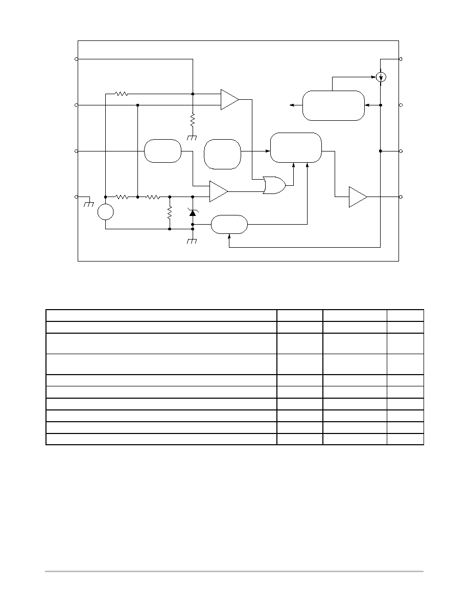
http://onsemi.com
3
-
+
-
+
-
+
250 ns
L.E.B.
40, 60 or
100 kHz
Clock
Overload?
Fault Duration
Skip Cycle
Comparator
1 V
V
ref
5.2 V
Q Flip-Flop
DCmax = 80%
±
110 mA
20 k
60 k
8 k
75.5 k
29 k
1.4 V
Reset
Q
Set
UVLO
High and Low
Internal Regulator
HV Current
Source
Internal
V
CC
4
3
2
1
Current
Sense
FB
Adj
Ground
Drv
V
CC
NC
HV
8
7
6
5
Figure 2. Internal Circuit Architecture
¡¡¡¡¡¡¡¡¡¡¡¡¡¡¡¡¡¡¡¡¡¡¡¡¡¡¡¡¡¡¡¡¡
¡¡¡¡¡¡¡¡¡¡¡¡¡¡¡¡¡¡¡¡¡¡¡¡¡¡¡¡¡¡¡¡¡
MAXIMUM RATINGS
¡¡¡¡¡¡¡¡¡¡¡¡¡¡¡¡¡¡¡¡¡
¡¡¡¡¡¡¡¡¡¡¡¡¡¡¡¡¡¡¡¡¡
Rating
¡¡¡¡¡
¡¡¡¡¡
Symbol
¡¡¡¡¡¡
¡¡¡¡¡¡
Value
¡¡¡¡
¡¡¡¡
Units
¡¡¡¡¡¡¡¡¡¡¡¡¡¡¡¡¡¡¡¡¡
¡¡¡¡¡¡¡¡¡¡¡¡¡¡¡¡¡¡¡¡¡
Power Supply Voltage
¡¡¡¡¡
¡¡¡¡¡
V
CC
¡¡¡¡¡¡
¡¡¡¡¡¡
16
¡¡¡¡
¡¡¡¡
V
¡¡¡¡¡¡¡¡¡¡¡¡¡¡¡¡¡¡¡¡¡
¡
¡¡¡¡¡¡¡¡¡¡¡¡¡¡¡¡¡¡¡
¡
¡¡¡¡¡¡¡¡¡¡¡¡¡¡¡¡¡¡¡¡¡
Thermal Resistance Junction-to-Air, PDIP-8 version
Thermal Resistance Junction-to-Air, SOIC version
¡¡¡¡¡
¡
¡¡¡
¡
¡¡¡¡¡
R
q
JA
R
q
JA
¡¡¡¡¡¡
¡
¡¡¡¡
¡
¡¡¡¡¡¡
100
178
¡¡¡¡
¡
¡¡
¡
¡¡¡¡
∞
C/W
¡¡¡¡¡¡¡¡¡¡¡¡¡¡¡¡¡¡¡¡¡
¡¡¡¡¡¡¡¡¡¡¡¡¡¡¡¡¡¡¡¡¡
Maximum Junction Temperature
Typical Temperature Shutdown
¡¡¡¡¡
¡¡¡¡¡
T
Jmax
-
¡¡¡¡¡¡
¡¡¡¡¡¡
150
140
¡¡¡¡
¡¡¡¡
∞
C
¡¡¡¡¡¡¡¡¡¡¡¡¡¡¡¡¡¡¡¡¡
¡¡¡¡¡¡¡¡¡¡¡¡¡¡¡¡¡¡¡¡¡
Storage Temperature Range
¡¡¡¡¡
¡¡¡¡¡
T
stg
¡¡¡¡¡¡
¡¡¡¡¡¡
-60 to +150
¡¡¡¡
¡¡¡¡
∞
C
¡¡¡¡¡¡¡¡¡¡¡¡¡¡¡¡¡¡¡¡¡
¡¡¡¡¡¡¡¡¡¡¡¡¡¡¡¡¡¡¡¡¡
ESD Capability, HBM Model (All Pins except V
CC
and HV)
¡¡¡¡¡
¡¡¡¡¡
-
¡¡¡¡¡¡
¡¡¡¡¡¡
2.0
¡¡¡¡
¡¡¡¡
kV
¡¡¡¡¡¡¡¡¡¡¡¡¡¡¡¡¡¡¡¡¡
¡¡¡¡¡¡¡¡¡¡¡¡¡¡¡¡¡¡¡¡¡
ESD Capability, Machine Model
¡¡¡¡¡
¡¡¡¡¡
-
¡¡¡¡¡¡
¡¡¡¡¡¡
200
¡¡¡¡
¡¡¡¡
V
¡¡¡¡¡¡¡¡¡¡¡¡¡¡¡¡¡¡¡¡¡
¡¡¡¡¡¡¡¡¡¡¡¡¡¡¡¡¡¡¡¡¡
Maximum Voltage on Pin 8 (HV), pin 6 (V
CC
) Grounded
¡¡¡¡¡
¡¡¡¡¡
-
¡¡¡¡¡¡
¡¡¡¡¡¡
450
¡¡¡¡
¡¡¡¡
V
¡¡¡¡¡¡¡¡¡¡¡¡¡¡¡¡¡¡¡¡¡
¡¡¡¡¡¡¡¡¡¡¡¡¡¡¡¡¡¡¡¡¡
Maximum Voltage on Pin 8 (HV), Pin 6 (V
CC
) Decoupled to Ground with 10
m
F
¡¡¡¡¡
¡¡¡¡¡
-
¡¡¡¡¡¡
¡¡¡¡¡¡
500
¡¡¡¡
¡¡¡¡
V
¡¡¡¡¡¡¡¡¡¡¡¡¡¡¡¡¡¡¡¡¡
¡¡¡¡¡¡¡¡¡¡¡¡¡¡¡¡¡¡¡¡¡
Minimum Operating Voltage on Pin 8 (HV)
¡¡¡¡¡
¡¡¡¡¡
-
¡¡¡¡¡¡
¡¡¡¡¡¡
30
¡¡¡¡
¡¡¡¡
V
Maximum ratings are those values beyond which device damage can occur. Maximum ratings applied to the device are individual stress limit
values (not normal operating conditions) and are not valid simultaneously. If these limits are exceeded, device functional operation is not implied,
damage may occur and reliability may be affected.

NCP1200
http://onsemi.com
4
ELECTRICAL CHARACTERISTICS
(For typical values T
J
= +25
∞
C, for min/max values T
J
= -25
∞
C to +125
∞
C, Max T
J
= 150
∞
C,
V
CC
= 11 V unless otherwise noted)
Rating
Pin
Symbol
Min
Typ
Max
Unit
DYNAMIC SELF-SUPPLY (All Frequency Versions, Otherwise Noted)
V
CC
Increasing Level at Which the Current Source Turns-off
6
V
CCOFF
10.3
11.4
12.5
V
V
CC
Decreasing Level at Which the Current Source Turns-on
6
V
CCON
8.8
9.8
11
V
V
CC
Decreasing Level at Which the Latchoff Phase Ends
6
V
CClatch
-
6.3
-
V
Internal IC Consumption, No Output Load on Pin 5
6
I
CC1
-
710
880
Note 1
m
A
Internal IC Consumption, 1 nF Output Load on Pin 5, F
SW
= 40 kHz
6
I
CC2
-
1.2
1.4
Note 2
mA
Internal IC Consumption, 1 nF Output Load on Pin 5, F
SW
= 60 kHz
6
I
CC2
-
1.4
1.6
Note 2
mA
Internal IC Consumption, 1 nF Output Load on Pin 5, F
SW
= 100 kHz
6
I
CC2
-
1.9
2.2
Note 2
mA
Internal IC Consumption, Latchoff Phase
6
I
CC3
-
350
-
m
A
INTERNAL CURRENT SOURCE
High-voltage Current Source, V
CC
= 10 V
8
I
C1
2.8
4.0
-
mA
High-voltage Current Source, V
CC
= 0 V
8
I
C2
-
4.9
-
mA
DRIVE OUTPUT
Output Voltage Rise-time @ CL = 1 nF, 10-90% of Output Signal
5
T
r
-
67
-
ns
Output Voltage Fall-time @ CL = 1 nF, 10-90% of Output Signal
5
T
f
-
28
-
ns
Source Resistance (drive = 0, Vgate = V
CCHMAX
- 1 V)
5
R
OH
27
40
61
W
Sink Resistance (drive = 11 V, Vgate = 1 V)
5
R
OL
5
12
25
W
CURRENT COMPARATOR (Pin 5 Un-loaded)
Input Bias Current @ 1 V Input Level on Pin 3
3
I
IB
-
0.02
-
m
A
Maximum internal Current Setpoint
3
I
Limit
0.8
0.9
1.0
V
Default Internal Current Setpoint for Skip Cycle Operation
3
I
Lskip
-
350
-
mV
Propagation Delay from Current Detection to Gate OFF State
3
T
DEL
-
100
160
ns
Leading Edge Blanking Duration
3
T
LEB
-
230
-
ns
INTERNAL OSCILLATOR (V
CC
= 11 V, Pin 5 Loaded by 1 k
W
)
Oscillation Frequency, 40 kHz Version
-
f
OSC
36
42
48
kHz
Oscillation Frequency, 60 kHz Version
-
f
OSC
52
61
70
kHz
Oscillation Frequency, 100 kHz Version
-
f
OSC
86
103
116
kHz
Built-in Frequency Jittering, F
SW
= 40 kHz
-
f
jitter
-
300
-
Hz/V
Built-in Frequency Jittering, F
SW
= 60 kHz
-
f
jitter
-
450
-
Hz/V
Built-in Frequency Jittering, F
SW
= 100 kHz
-
f
jitter
-
620
-
Hz/V
Maximum Duty Cycle
-
Dmax
74
80
87
%
FEEDBACK SECTION (V
CC
= 11 V, Pin 5 Loaded by 1 k
W
)
Internal Pullup Resistor
2
Rup
-
8.0
-
k
W
Pin 3 to Current Setpoint Division Ratio
-
Iratio
-
4.0
-
-
SKIP CYCLE GENERATION
Default skip mode level
1
Vskip
1.1
1.4
1.6
V
Pin 1 internal output impedance
1
Zout
-
25
-
k
W
1. Max value @ T
J
= -25
∞
C.
2. Max value @ T
J
= 25
∞
C, please see characterization curves.
NCP1200
http://onsemi.com
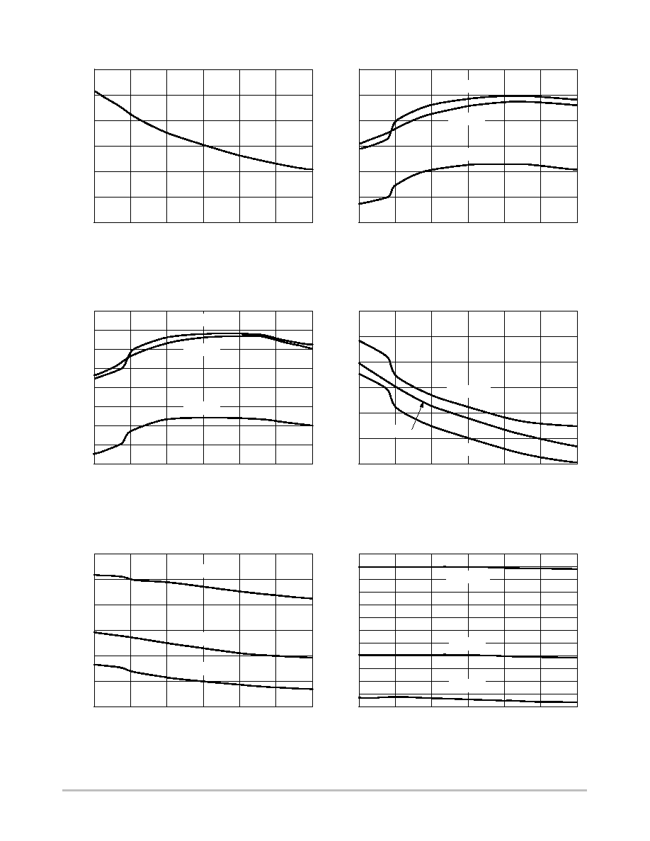
5
-25
75
50
25
100
125
0
-25
75
50
25
100
125
0
2.10
1.90
1.50
1.70
1.30
1.10
0.90
74
62
80
56
68
38
86
92
98
104
110
11.50
11.30
11.60
11.20
11.40
11.70
750
-25
60
75
30
50
25
LEAKAGE (
m
A)
0
TEMPERATURE (
∞
C)
Figure 3. HV Pin Leakage Current vs.
Temperature
Figure 4. V
CC
OFF vs. Temperature
V
CCOFF
(V)
9.85
9.80
9.75
9.70
9.65
9.60
9.55
9.50
9.45
Figure 5. V
CC
ON vs. Temperature
TEMPERATURE (
∞
C)
Figure 6. I
CC1
vs. Temperature
TEMPERATURE (
∞
C)
I
CC1
(
m
A)
V
CCON
(V)
Figure 7. I
CC2
vs. Temperature
TEMPERATURE (
∞
C)
Figure 8. Switching Frequency vs. T
J
TEMPERATURE (
∞
C)
I
CC2
(mA)
F
SW
(kHz)
650
800
700
600
850
900
100 kHz
TEMPERATURE (
∞
C)
10
20
40
50
100
125
11.10
0
-25
75
50
25
100
125
0
40 kHz
60 kHz
100 kHz
40 kHz
60 kHz
100 kHz
40 kHz
60 kHz
-25
75
50
25
100
125
0
100 kHz
40 kHz
60 kHz
50
44
-25
75
50
25
100
125
0
100 kHz
40 kHz
60 kHz