©
Semiconductor Components Industries, LLC, 2004
October, 2004- Rev. 4
1
Publication Order Number:
NCP1203/D
NCP1203
PWM Current-Mode
Controller for Universal
Off-Line Supplies Featuring
Standby and Short Circuit
Protection
Housed in SOIC-8 or PDIP-8 package, the NCP1203 represents a
major leap toward ultra-compact Switchmode Power Supplies and
represents an excellent candidate to replace the UC384X devices. Due
to its proprietary SMARTMOS
t Very High Voltage Technology, the
circuit allows the implementation of complete off-line AC-DC
adapters, battery charger and a high-power SMPS with few external
components.
With an internal structure operating at a fixed 40 kHz, 60 kHz or
100 kHz switching frequency, the controller features a high-voltage
startup FET which ensures a clean and loss-less startup sequence. Its
current-mode control naturally provides good audio-susceptibility
and inherent pulse-by-pulse control.
When the current setpoint falls below a given value, e.g. the output
power demand diminishes, the IC automatically enters the so-called
skip cycle mode and provides improved efficiency at light loads
while offering excellent performance in standby conditions. Because
this occurs at a user adjustable low peak current, no acoustic noise
takes place.
The NCP1203 also includes an efficient protective circuitry which,
in presence of an output over load condition, disables the output
pulses while the device enters a safe burst mode, trying to restart.
Once the default has gone, the device auto-recovers. Finally, a
temperature shutdown with hysteresis helps building safe and robust
power supplies.
Features
∑
Pb-Free Packages are Available
∑
High-Voltage Startup Current Source
∑
Auto-Recovery Internal Output Short-Circuit Protection
∑
Extremely Low No-Load Standby Power
∑
Current-Mode with Adjustable Skip-Cycle Capability
∑
Internal Leading Edge Blanking
∑
250 mA Peak Current Capability
∑
Internally Fixed Frequency at 40 kHz, 60 kHz and 100 kHz
∑
Direct Optocoupler Connection
∑
Undervoltage Lockout at 7.8 V Typical
∑
SPICE Models Available for TRANsient and AC Analysis
∑
Pin to Pin Compatible with NCP1200
Applications
∑
AC-DC Adapters for Notebooks, etc.
∑
Offline Battery Chargers
∑
Auxiliary Power Supplies (USB, Appliances, TVs, etc.)
SOIC-8
D1, D2 SUFFIX
CASE 751
1
8
MARKING
DIAGRAMS
PIN CONNECTIONS
PDIP-8
N SUFFIX
CASE 626
1
8
xx
= Specific Device Code
A
= Assembly Location
WL, L
= Wafer Lot
Y, YY
= Year
W, WW = Work Week
1
Adj
8 HV
2
FB
3
CS
4
GND
7 NC
6 V
CC
5 Drv
(Top View)
xxxxxxxxx
AWL
YYWW
1
8
See detailed ordering and shipping information in the package
dimensions section on page 12 of this data sheet.
ORDERING INFORMATION
http://onsemi.com
xxxxxx
ALYW
G
1
8

NCP1203
http://onsemi.com
2
Figure 1. Typical Application Example
EMI
FILTER
UNIVERSAL
INPUT
+
+
NCP1203
+
V
OUT
Aux.
Adj
FB
CS
GND
HV
V
CC
Drv
1
2
3
4
8
7
6
5
*
*Please refer to the application information section
PIN FUNCTION DESCRIPTION
Pin No.
Pin Name
Function
Pin Description
1
Adj
Adjust the skipping peak current
This pin lets you adjust the level at which the cycle skipping process takes
place. Shorting this pin to ground, permanently disables the skip cycle
feature.
2
FB
Sets the peak current setpoint
By connecting an optocoupler to this pin, the peak current setpoint is
adjusted accordingly to the output power demand. Skip cycle occurs when
FB falls below Vpin1.
3
CS
Current sense input
This pin senses the primary current and routes it to the internal comparator
via an L.E.B.
4
GND
The IC ground
-
5
Drv
Driving pulses
The driver's output to an external MOSFET.
6
V
CC
Supplies the IC
This pin is connected to an external bulk capacitor of typically 22
m
F.
7
NC
-
This unconnected pin ensures adequate creepage distance.
8
HV
Ensure a clean and lossless
startup sequence
Connected to the high-voltage rail, this pin injects a constant current into
the V
CC
capacitor during the startup sequence.
NCP1203
http://onsemi.com
3
Figure 2. Internal Circuit Architecture
OVERLOAD
MANAGEMENT
UVLO HIGH AND LOW
INTERNAL REGULATOR
±
250 mA
HV CURRENT
SOURCE
INTERNAL V
CC
8
7
6
5
HV
NC
V
CC
Drv
1
2
3
4
Q FLIP-FLOP
DCmax = 80%
Q
250 ns
L.E.B.
40-60-100 kHz
CLOCK
-
+
-
+
80 k
20 k
57 k
1 V
CURRENT
SENSE
GROUND
FB
Adj
24 k
25 k
+
-
V
REF
RESET
1.2 V
SKIP CYCLE
COMPARATOR
SET
MAXIMUM RATINGS
Rating
Symbol
Value
Unit
Power Supply Voltage
V
CC
, Drv
16
V
Power Supply Voltage on all other pins except Pin 5 (Drv), Pin 6 (V
CC
) and Pin 8 (HV)
-
-0.3 to 10
V
Maximum Current into all pins except Pin 6 (V
CC
) and Pin 8 (HV) when
10 V ESD diodes are activated
-
5.0
mA
Thermal Resistance Junction-to-Air, PDIP-8 Version
Thermal Resistance Junction-to-Air, SOIC Version
R
q
JA
R
q
JA
100
178
∞
C/W
∞
C/W
Maximum Junction Temperature
TJ
MAX
150
∞
C
Temperature Shutdown
-
170
∞
C
Hysteresis in Shutdown
-
30
∞
C
Storage Temperature Range
-
-60 to +150
∞
C
ESD Capability, HBM Model, All pins except Pin 6 (V
CC
) and Pin 8 (HV)
-
2.0
KV
ESD Capability, Machine Model
-
200
V
Maximum Voltage on Pin 6 (V
CC
) and Pin 8 (HV) Decoupled to Ground with 10
m
F
-
450
V
Maximum ratings are those values beyond which device damage can occur. Maximum ratings applied to the device are individual stress limit
values (not normal operating conditions) and are not valid simultaneously. If these limits are exceeded, device functional operation is not implied,
damage may occur and reliability may be affected.
NCP1203
http://onsemi.com
4
ELECTRICAL CHARACTERISTICS
(For typical values T
J
= 25
∞
C, for min/max values T
J
= 0
∞
C to +125
∞
C, Max T
J
= 150
∞
C,
V
CC
= 11 V unless otherwise noted.)
Characteristic
Symbol
Pin
Min
Typ
Max
Unit
Supply Section (All frequency versions, otherwise noted)
Turn-on Threshold Level, V
CC
Going Up
V
CC(on)
6
12.2
12.8
14
V
Minimum Operating Voltage after Turn-on
V
CC(min)
6
7.2
7.8
8.4
V
V
CC
Decreasing Level at which the Latchoff Phase Ends
V
CClatch
6
-
4.9
-
V
Internal IC Consumption, No Output Load on Pin 5
ICC1
6
-
750
880
(Note 1)
m
A
Internal IC Consumption, 1.0 nF Output Load on Pin 5,
F
SW
= 40 kHz
ICC2
6
-
1.2
1.4
(Note 2)
mA
Internal IC Consumption, 1.0 nF Output Load on Pin 5,
F
SW
= 60 kHz
ICC2
6
-
1.4
1.6
(Note 2)
mA
Internal IC Consumption, 1.0 nF Output Load on Pin 5,
F
SW
= 100 kHz
ICC2
6
-
2.0
2.2
(Note 2)
mA
Internal IC Consumption, Latch-off Phase, V
CC
= 6.0 V
ICC3
6
-
250
-
m
A
Internal Startup Current Source (Pin 8 biased at 50 V)
High-Voltage Current Source, V
CC
= 10 V
IC1
8
3.5
6.0
9.0
mA
High-Voltage Current Source, V
CC
= 0
IC2
8
-
11
-
mA
Drive Output
Output Voltage Rise-Time @ CL = 1.0 nF, 10-90% of
Output Signal
T
r
5
-
67
-
ns
Output Voltage Fall-Time @ CL = 1.0 nF, 10-90% of
Output Signal
T
f
5
-
28
-
ns
Source Resistance
R
OH
5
27
40
61
W
Sink Resistance
R
OL
5
5.0
10
20
W
Current Comparator (Pin 5 loaded unless otherwise noted)
Input Bias Current @ 1.0 V Input Level on Pin 3
I
IB
3
-
0.02
-
m
A
Maximum Internal Current Setpoint (Note 3)
I
Limit
3
0.85
0.92
1.0
V
Default Internal Current Setpoint for Skip Cycle Operation
I
Lskip
3
-
360
-
mV
Propagation Delay from Current Detection to Gate OFF
State
T
DEL
3
-
90
160
ns
Leading Edge Blanking Duration (Note 3)
T
LEB
3
-
230
-
ns
Internal Oscillator (V
CC
= 11 V, Pin 5 loaded by 1 nF)
Oscillation Frequency, 40 kHz Version
f
OSC
-
37
42
47
kHz
Oscillation Frequency, 60 kHz Version
f
OSC
-
57
65
73
kHz
Oscillation Frequency, 100 kHz Version
f
OSC
-
90
103
115
kHz
Maximum Duty-Cycle
Dmax
-
74
80
87
%
Feedback Section (V
CC
= 11 V, Pin 5 unloaded)
Internal Pullup Resistor
Rup
2
-
20
-
k
W
Pin 3 to Current Setpoint Division Ratio
Iratio
-
-
3.3
-
-
Skip Cycle Generation
Default Skip Mode Level
Vskip
1
1.0
1.2
1.4
V
Pin 1 Internal Output Impedance
Zout
1
-
22
-
k
W
1. Max value at T
J
= 0
∞
C.
2. Maximum value @ T
J
= 25
∞
C, please see characterization curves.
3. Pin 5 loaded by 1 nF.
NCP1203
http://onsemi.com
5
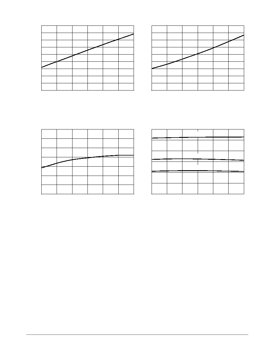
TEMPERATURE (
∞
C)
125
100
75
50
25
0
-25
150
200
250
300
350
400
I
CC
@ V
CC
= 6 V (
m
A)
Figure 3. V
CC(on)
Threshold versus
Temperature
Figure 4. V
CC(min)
Level versus Temperature
8.4
8.2
-25
0
8.0
7.6
7.2
125
-25
14.0
13.8
50
12.6
12.4
12.2
100
7.4
25
25
0
125
TEMPERATURE (
∞
C)
TEMPERATURE (
∞
C)
V
CC(min)
LEVEL (V)
V
CC(on)
THRESHOLD (V)
75
13.0
12.8
13.2
13.6
13.4
50
75
100
7.8
Figure 5. I
C
Current Consumption (No Load)
versus Temperature
Figure 6. I
CC
Consumption (Loaded by 1 nF)
versus Temperature
TEMPERATURE (
∞
C)
Figure 7. HV Current Source at V
CC
= 10 V
versus Temperature
Figure 8. I
C
Consumption at V
CC
= 6 V
versus Temperature
TEMPERATURE (
∞
C)
TEMPERATURE (
∞
C)
125
100
75
50
25
0
-25
500
550
600
650
700
750
950
1000
I
CC
, CURRENT CONSUMPTION (
m
A)
800
850
900
100 kHz
60 kHz
40 kHz
125
100
75
50
25
0
-25
1.0
1.2
1.4
1.6
1.8
2.0
I
CC
, 1 nF LOAD CONSUMPTION (mA)
100 kHz
60 kHz
40 kHz
125
100
75
50
25
0
-25
4.0
4.5
5.0
5.5
6.0
6.5
7.5
8.0
7.0
HV CURRENT SOURCE (mA)
100 kHz
40 & 60 kHz
NCP1203
http://onsemi.com
6
Figure 9. Drive Source Resistance versus
Temperature
Figure 10. Drive Sink Resistance versus
Temperature
20
16
-25
0
14
6
2
125
-25
60
50
50
25
20
15
100
4
25
25
0
125
TEMPERATURE (
∞
C)
TEMPERATURE (
∞
C)
DRIVE SINK RESIST
ANCE (
W
)
DRIVE SOURCE RESIST
ANCE (
W
)
75
30
35
45
40
50
75
100
8
Figure 11. Maximum Current Setpoint versus
Temperature
Figure 12. Frequency versus Temperature
-25
0.99
0.97
50
0.89
0.87
0.85
100
25
0
125
TEMPERATURE (
∞
C)
TEMPERATURE (
∞
C)
MAXIMUM CURRENT SETPOINT (V)
75
0.91
0.93
0.95
55
10
12
18
125
100
75
50
25
0
-25
0
20
40
60
80
100
120
f, FREQUENCY (kHz)
100 kHz
60 kHz
40 kHz

NCP1203
http://onsemi.com
7
APPLICATION INFORMATION
Introduction
The NCP1203 implements a standard current mode
architecture where the switch-off time is dictated by the
peak current setpoint. This component represents the ideal
candidate where low part-count is the key parameter,
particularly in low-cost AC-DC adapters, auxiliary
supplies etc. Due to its high-performance SMARTMOS
High-Voltage technology, the NCP1203 incorporates all the
necessary components normally needed in UC384X based
supplies: timing components, feedback devices, low-pass
filter and startup device. This later point emphasizes the fact
that ON Semiconductor's NCP1203 does not need an
external startup resistance but supplies the startup current
directly from the high-voltage rail. On the other hand, more
and more applications are requiring low no-load standby
power, e.g. for AC-DC adapters, VCRs etc. UC384X series
have a lot of difficulty to reduce the switching losses at low
power levels. NCP1203 elegantly solves this problem by
skipping unwanted switching cycles at a user-adjustable
power level. By ensuring that skip cycles take place at low
peak current, the device ensures quiet, noise free operation.
Finally, an auto-recovery output short-circuit protection
(OCP) prevents from any lethal thermal runaway in
overload conditions.
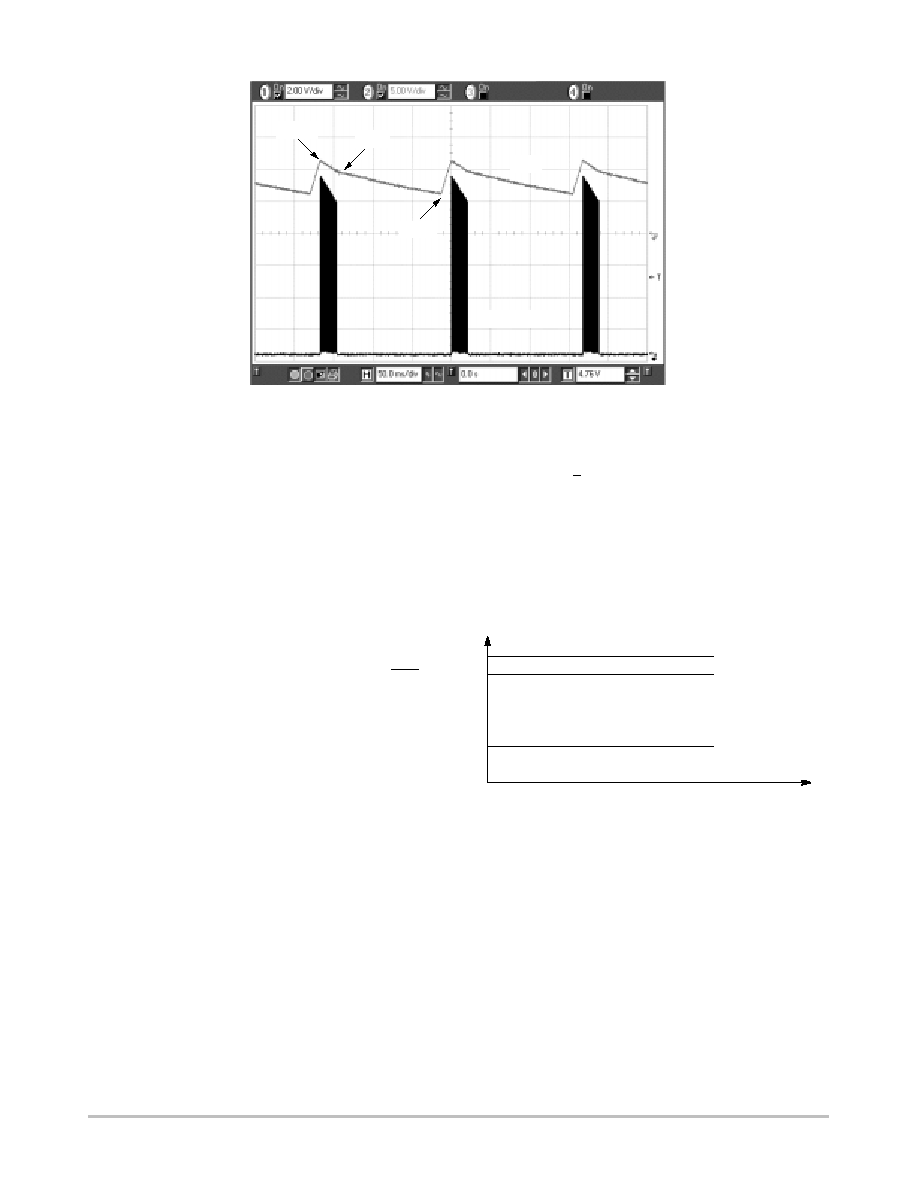
Startup Sequence
When the power supply is first powered from the mains
outlet, the internal current source (typically 6.0 mA) is
biased and charges up the V
CC
capacitor. When the voltage
on this V
CC
capacitor reaches the V
CC(on)
level (typically
12.8 V), the current source turns off and no longer wastes
any power. At this time, the V
CC
capacitor only supplies the
controller and the auxiliary supply is supposed to take over
before V
CC
collapses below V
CC(min)
. Figure 13 shows the
internal arrangement of this structure:
Figure 13. The Current Source Brings V
CC
Above 12.8 V and then Turns Off
-
+
8
6
4
6 mA or 0
CV
CC
Aux
HV
12.8 V/4.9 V
Once the power supply has started, the V
CC
shall be
constrained below 16 V, which is the maximum rating on
pin 6. Figure 14 portrays a typical startup sequence with a
V
CC
regulated at 12.5 V:
Figure 14. A Typical Startup Sequence for
the NCP1203
t, TIME (sec)
3.00 M
8.00 M
13.0 M
18.0 M
23.0 M
13.5
12.5
11.5
10.5
9.5
REGULATION
12.8 V

NCP1203
http://onsemi.com
8
Current-Mode Operation
As the UC384X series, the NCP1203 features a
well-known current mode control architecture which
provides superior input audio-susceptibility compared to
traditional voltage-mode controllers. Primary current
pulse-by-pulse checking together with a fast over current
comparator offers greater security in the event of a difficult
fault condition, e.g. a saturating transformer.
Adjustable Skip Cycle Level
By offering the ability to tailor the level at which the skip
cycle takes place, the designer can make sure that the skip
operation only occurs at low peak current. This point
guarantees a noise-free operation with cheap transformers.
Skip cycle offers a proven mean to reduce the standby power
in no or light loads situations.
Wide Switching-Frequency Offer
Four different options are available: 40 kHz - 65 kHz ≠
100 kHz. Depending on the application, the designer can
pick up the right device to help reducing magnetics or
improve the EMI signature before reaching the 150 kHz
starting point.
Overcurrent Protection (OCP)
When the auxiliary winding collapses below UVLOlow,
the controller stops switching and reduces its consumption.
It stays in this mode until Vcc reaches 4.9 V typical, where
the startup source is reactivated and a new startup sequence
is attempted. The power supply is thus operated in burst
mode and avoids any lethal thermal runaway. When the
default goes way, the power supply automatically resumes
operation.
Wide Duty-Cycle Operation
Wide mains operation requires a large duty-cycle
excursion. The NCP1203 can go up to 80% typically.
Low Standby Power
If SMPS naturally exhibit a good efficiency at nominal
load, they begin to be less efficient when the output power
demand diminishes. By skipping un-needed switching
cycles, the NCP1203 drastically reduces the power wasted
during light load conditions. In no-load conditions, the
NCP1203 allows the total standby power to easily reach next
International Energy Agency (IEA) recommendations.
No Acoustic Noise while Operating
Instead of skipping cycles at high peak currents, the
NCP1203 waits until the peak current demand falls below a
user-adjustable 1/3
rd
of the maximum limit. As a result,
cycle skipping can take place without having a singing
transformer
...
You can thus select cheap magnetic
components free of noise problems.
External MOSFET Connection
By leaving the external MOSFET external to the IC, you
can select avalanche proof devices which, in certain cases
(e.g. low output powers), let you work without an active
clamping network. Also, by controlling the MOSFET gate
signal flow, you have an option to slow down the device
commutation, therefore reducing the amount of
ElectroMagnetic Interference (EMI).
SPICE Model
A dedicated model to run transient cycle-by-cycle
simulations is available but also an averaged version to help
you closing the loop. Ready-to-use templates can be
downloaded in OrCAD's Pspice and INTUSOFT's from ON
Semiconductor web site, NCP1203 related section.
Overload Operation
In applications where the output current is purposely not
controlled (e.g. wall adapters delivering raw DC level), it is
interesting to implement a true short-circuit protection. A
short-circuit actually forces the output voltage to be at a low
level, preventing a bias current to circulate in the
optocoupler LED. As a result, the auxiliary voltage also
decreases because it also operates in Flyback and thus
duplicates the output voltage, providing the leakage
inductance
between windings is kept low. To account for this
situation and properly protect the power supply, NCP1203
hosts a dedicated overload detection circuitry. Once
activated, this circuitry imposes to deliver pulses in a burst
manner with a low duty-cycle. The system auto-recovers
when the fault condition disappears.
During the startup phase, the peak current is pushed to the
maximum until the output voltage reaches its target and the
feedback loop takes over. The auxiliary voltage takes place
after a few switching cycles and self-supplies the IC. In
presence of a short circuit on the output, the auxiliary
voltage will go down until it crosses the undervoltage
lockout level of typically 7.8 V. When this happens,
NCP1203 immediately stops the switching pulses and
unbias all unnecessary logical blocks. The overall
consumption drops, while keeping the gate grounded, and
the V
CC
slowly falls down. As soon as V
CC
reaches typically
4.8 V, the startup source turns-on again and a new startup
sequence occurs, bringing V
CC
toward 12.8 V as an attempt
to restart. If the default has gone, then the power supply
normally restarts. If not, a new protective burst is initiated,
shielding the SMPS from any runaway. Figure 15, on the
following page, portrays the typical operating signals in
short circuit.
NCP1203
http://onsemi.com
9
Figure 15. Typical Waveforms in Short Circuit Conditions
7.8 V
12.8 V
4.9 V
V
CC
DRIVING PULSES
Calculating the V
CC
Capacitor
The V
CC
capacitor can be calculated knowing the IC
consumption as soon as V
CC
reaches 12.8 V. Suppose that a
NCP1203P60 is used and drives a MOSFET with a 30 nC
total gate charge (Qg). The total average current is thus made
of ICC1 (700
mA) plus the driver current, Fsw x Qg or
1.8 mA. The total current is therefore 2.5 mA. The
DV
available to fully startup the circuit (e.g. never reach the
7.8 V UVLO during power on) is 12.8≠7.8 = 5 V. We have
a capacitor who then needs to supply the NCP1203 with
2.5 mA during a given time until the auxiliary supply takes
over. Suppose that this time was measured at around 15 ms.
CV
CC
is calculated using the equation
C
+
D
t ∑ i
D
V
or
C
w
7.5
m
F
. Select a 22
mF/16 V and this will fit.
Skipping Cycle Mode
The NCP1203 automatically skips switching cycles when
the output power demand drops below a given level. This is
accomplished by monitoring the FB pin. In normal
operation, pin 2 imposes a peak current accordingly to the
load value. If the load demand decreases, the internal loop
asks for less peak current. When this setpoint reaches a
determined level (Vpin 1), the IC prevents the current from
decreasing further down and starts to blank the output
pulses: the IC enters the so-called skip cycle mode, also
named controlled burst operation. The power transfer now
depends upon the width of the pulse bunches (Figure 17).
Suppose we have the following component values:
Lp, primary inductance = 350
mH
Fsw , switching frequency = 61 kHz
Ip skip = 600 mA (or 333 mV/Rsense)
The theoretical power transfer is therefore:
1
2
∑ Lp ∑ Ip2 ∑ Fsw
+
3.8 W
If this IC enters skip cycle mode with a bunch length of
10 ms over a recurrent period of 100 ms, then the total power
transfer is:
3.8 . 0.1
+
380 mW
.
To better understand how this skip cycle mode takes place,
a look at the operation mode versus the FB level
immediately gives the necessary insight:
Figure 16.
SKIP CYCLE OPERATION
I
P(min)
= 333 mV/R
SENSE
NORMAL CURRENT
MODE OPERATION
FB
1 V
4.2 V, FB Pin Open
3.2 V, Upper
Dynamic Range
When FB is above the skip cycle threshold (1.0 V by
default), the peak current cannot exceed 1.0 V/Rsense.
When the IC enters the skip cycle mode, the peak current
cannot go below Vpin1/3.3/Rsense. The user still has the
flexibility to alter this 1.0 V by either shunting pin 1 to
ground through a resistor or raising it through a resistor up
to the desired level. Grounding pin 1 permanently
invalidates the skip cycle operation. However, given the
extremely low standby power the controller can reach, the
PWM in no-load conditions can quickly enter the minimum
t
on
and still transfer too much power. An instability can take
place. We recommend in that case to leave a little bit of skip
level to always allow 0% duty cycle.
NCP1203
http://onsemi.com
10
Power P1
Power P2
Power P3
Figure 17. Output Pulses at Various Power Levels (X = 5.0
m
s/div) P1
t
P2
t
P3
Figure 18. The Skip Cycle Takes Place at Low Peak Currents which Guaranties Noise-Free Operation
315.40
882.70
1.450 M
2.017 M
2.585 M
300 M
200 M
100 M
0
MAX PEAK
CURRENT
SKIP CYCLE
CURRENT LIMIT
We recommend a pin 1 operation between 400 mV and
1.3 V that will fix the skip peak current level between
120 mV/Rsense and 390 mV/Rsense.
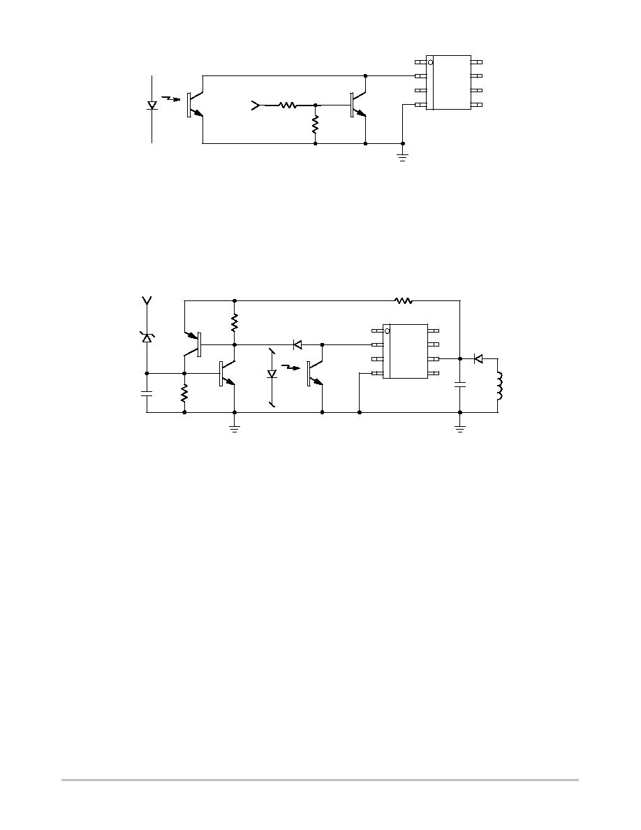
Non-Latching Shutdown
In some cases, it might be desirable to shut off the part
temporarily and authorize its restart once the default has
disappeared. This option can easily be accomplished
through a single NPN bipolar transistor wired between FB
and ground. By pulling FB below the Adj pin 1 level, the
output pulses are disabled as long as FB is pulled below
pin 1. As soon as FB is relaxed, the IC resumes its operation.
Figure 19 depicts the application example.
NCP1203
http://onsemi.com
11
Figure 19. Another Way of Shutting Down the IC without a Definitive Latch-Off State
ON/OFF
Q1
8
7
6
5
1
2
3
4
Full Latching Shutdown
Other applications require a full latching shutdown, e.g.
when an abnormal situation is detected (overtemperature or
overvoltage). This feature can easily be implemented
through two external transistors wired as a discrete SCR.
When the V
CC
level exceeds the zener breakdown voltage,
the NPN biases the PNP and fires the equivalent SCR,
permanently bringing down the FB pin. The switching
pulses are disabled until the user unplugs the power supply.
Figure 20. Two Bipolars Ensure a Total Latch-Off of the SMPS in Presence of an OVP
LAux
NCP1203
CV
CC
Rhold
12 k
0.1
m
F
10 k
10 k
8
7
6
5
1
2
3
4
OVP
Rhold ensures that the SCR stays on when fired. The bias
current flowing through Rhold should be small enough to let
the V
CC
ramp up (12.8 V) and down (4.9 V) when the SCR
is fired. The NPN base can also receive a signal from a
temperature sensor. Typical bipolars can be MMBT2222
and MMBT2907 for the discrete latch. The MMBT3946
features two bipolars NPN+PNP in the same package and
could also be used.
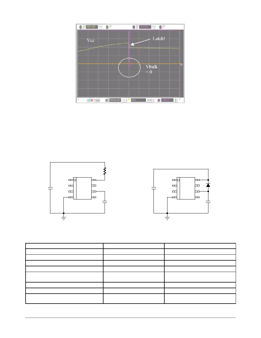
Protecting the Controller Against Negative Spikes
As with any controller built upon a CMOS technology, it
is the designer's duty to avoid the presence of negative
spikes on sensitive pins. Negative signals have the bad habit
to forward bias the controller substrate and induce erratic
behaviors. Sometimes, the injection can be so strong that
internal parasitic SCRs are triggered, engendering
irremediable damages to the IC if they are a low impedance
path is offered between V
CC
and GND. If the current sense
pin is often the seat of such spurious signals, the
high-voltage pin can also be the source of problems in
certain circumstances. During the turn-off sequence, e.g.
when the user un-plugs the power supply, the controller is
still fed by its V
CC
capacitor and keeps activating the
MOSFET ON and OFF with a peak current limited by
Rsense. Unfortunately, if the quality coefficient Q of the
resonating network formed by Lp and Cbulk is low (e.g. the
MOSFET Rdson + Rsense are small), conditions are met to
make the circuit resonate and thus negatively bias the
controller. Since we are talking about ms pulses, the amount
of injected charge (Q = I x t) immediately latches the
controller which brutally discharges its V
CC
capacitor. If this
V
CC
capacitor is of sufficient value, its stored energy
damages the controller. Figure 21 depicts a typical negative
shot occurring on the HV pin where the brutal V
CC
discharge
testifies for latchup.
NCP1203
http://onsemi.com
12
Figure 21. A negative spike takes place on the Bulk capacitor at the switch-off sequence
Simple and inexpensive cures exist to prevent from
internal parasitic SCR activation. One of them consists in
inserting a resistor in series with the high-voltage pin to
keep the negative current to the lowest when the bulk
becomes negative (Figure 22). Please note that the negative
spike is clamped to ≠2 x Vf due to the diode bridge. Also, the
power dissipation of this resistor is extremely small since it
only heats up during the startup sequence.
Another option (Figure 23) consists in wiring a diode from
V
CC
to the bulk capacitor to force V
CC
to reach UVLOlow
sooner and thus stops the switching activity before the bulk
capacitor gets deeply discharged. For security reasons, two
diodes can be connected in series.
Figure 22. A simple resistor in series avoids any
latchup in the controller
CV
CC
D3
1N4007
8
7
6
5
1
2
3
4
+
Cbulk
+
CV
CC
Rbulk
> 4.7 k
8
7
6
5
1
2
3
4
+
Cbulk
+
Figure 23. or a diode forces V
CC
to reach
UVLOlow sooner
ORDERING INFORMATION
Device
Package
Shipping
NCP1203P40
PDIP-8
50 Units / Tube
NCP1203D40R2
SOIC-8
2500 Units / Tape & Reel
NCP1203P60
PDIP-8
50 Units / Tube
NCP1203D60R2
SOIC-8
2500 Units / Tape & Reel
NCP1203D60R2G
SOIC-8
(Pb-Free)
2500 Units / Tape & Reel
NCP1203P100
PDIP-8
50 Units / Tube
NCP1203D100R2
SOIC-8
2500 Units / Tape & Reel
NCP1203D100R2G
SOIC-8
(Pb-Free)
2500 Units / Tape & Reel
For information on tape and reel specifications, including part orientation and tape sizes, please refer to our Tape and Reel Packaging
Specifications Brochure, BRD8011/D.
NCP1203
http://onsemi.com
13
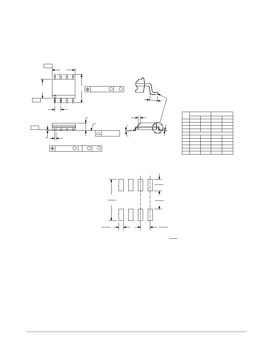
PACKAGE DIMENSIONS
SOIC-8
D1, D2 SUFFIX
CASE 751-07
ISSUE AC
*For additional information on our Pb-Free strategy and soldering
details, please download the ON Semiconductor Soldering and
Mounting Techniques Reference Manual, SOLDERRM/D.
SOLDERING FOOTPRINT*
SEATING
PLANE
1
4
5
8
N
J
X 45
_
K
NOTES:
1. DIMENSIONING AND TOLERANCING PER
ANSI Y14.5M, 1982.
2. CONTROLLING DIMENSION: MILLIMETER.
3. DIMENSION A AND B DO NOT INCLUDE
MOLD PROTRUSION.
4. MAXIMUM MOLD PROTRUSION 0.15 (0.006)
PER SIDE.
5. DIMENSION D DOES NOT INCLUDE DAMBAR
PROTRUSION. ALLOWABLE DAMBAR
PROTRUSION SHALL BE 0.127 (0.005) TOTAL
IN EXCESS OF THE D DIMENSION AT
MAXIMUM MATERIAL CONDITION.
6. 751-01 THRU 751-06 ARE OBSOLETE. NEW
STANDARD IS 751-07.
A
B
S
D
H
C
0.10 (0.004)
DIM
A
MIN
MAX
MIN
MAX
INCHES
4.80
5.00
0.189
0.197
MILLIMETERS
B
3.80
4.00
0.150
0.157
C
1.35
1.75
0.053
0.069
D
0.33
0.51
0.013
0.020
G
1.27 BSC
0.050 BSC
H
0.10
0.25
0.004
0.010
J
0.19
0.25
0.007
0.010
K
0.40
1.27
0.016
0.050
M
0
8
0
8
N
0.25
0.50
0.010
0.020
S
5.80
6.20
0.228
0.244
-X-
-Y-
G
M
Y
M
0.25 (0.010)
-Z-
Y
M
0.25 (0.010)
Z
S
X
S
M
_
_
_
_
1.52
0.060
7.0
0.275
0.6
0.024
1.270
0.050
4.0
0.155
mm
inches
SCALE 6:1

NCP1203
http://onsemi.com
14
PACKAGE DIMENSIONS
PDIP-8
N SUFFIX
CASE 626-05
ISSUE L
NOTES:
1. DIMENSION L TO CENTER OF LEAD WHEN
FORMED PARALLEL.
2. PACKAGE CONTOUR OPTIONAL (ROUND OR
SQUARE CORNERS).
3. DIMENSIONING AND TOLERANCING PER ANSI
Y14.5M, 1982.
1
4
5
8
F
NOTE 2
-A-
-B-
-T-
SEATING
PLANE
H
J
G
D
K
N
C
L
M
M
A
M
0.13 (0.005)
B
M
T
DIM
MIN
MAX
MIN
MAX
INCHES
MILLIMETERS
A
9.40
10.16
0.370
0.400
B
6.10
6.60
0.240
0.260
C
3.94
4.45
0.155
0.175
D
0.38
0.51
0.015
0.020
F
1.02
1.78
0.040
0.070
G
2.54 BSC
0.100 BSC
H
0.76
1.27
0.030
0.050
J
0.20
0.30
0.008
0.012
K
2.92
3.43
0.115
0.135
L
7.62 BSC
0.300 BSC
M
---
10
---
10
N
0.76
1.01
0.030
0.040
_
_
ON Semiconductor and are registered trademarks of Semiconductor Components Industries, LLC (SCILLC). SCILLC reserves the right to make changes without further notice
to any products herein. SCILLC makes no warranty, representation or guarantee regarding the suitability of its products for any particular purpose, nor does SCILLC assume any liability
arising out of the application or use of any product or circuit, and specifically disclaims any and all liability, including without limitation special, consequential or incidental damages.
"Typical" parameters which may be provided in SCILLC data sheets and/or specifications can and do vary in different applications and actual performance may vary over time. All
operating parameters, including "Typicals" must be validated for each customer application by customer's technical experts. SCILLC does not convey any license under its patent rights
nor the rights of others. SCILLC products are not designed, intended, or authorized for use as components in systems intended for surgical implant into the body, or other applications
intended to support or sustain life, or for any other application in which the failure of the SCILLC product could create a situation where personal injury or death may occur. Should
Buyer purchase or use SCILLC products for any such unintended or unauthorized application, Buyer shall indemnify and hold SCILLC and its officers, employees, subsidiaries, affiliates,
and distributors harmless against all claims, costs, damages, and expenses, and reasonable attorney fees arising out of, directly or indirectly, any claim of personal injury or death
associated with such unintended or unauthorized use, even if such claim alleges that SCILLC was negligent regarding the design or manufacture of the part. SCILLC is an Equal
Opportunity/Affirmative Action Employer. This literature is subject to all applicable copyright laws and is not for resale in any manner.
PUBLICATION ORDERING INFORMATION
N. American Technical Support: 800-282-9855 Toll Free
USA/Canada
Japan: ON Semiconductor, Japan Customer Focus Center
2-9-1 Kamimeguro, Meguro-ku, Tokyo, Japan 153-0051
Phone: 81-3-5773-3850
NCP1203/D
The product described herein (NCP1203), may be covered by the following U.S. patents: 6,271,735, 6,362,067, 6,385,060, 6,429,709, 6,587,357. There may
be other patents pending.
SMARTMOS is a trademark of Motorola, Inc.
LITERATURE FULFILLMENT:
Literature Distribution Center for ON Semiconductor
P.O. Box 61312, Phoenix, Arizona 85082-1312 USA
Phone: 480-829-7710 or 800-344-3860 Toll Free USA/Canada
Fax: 480-829-7709 or 800-344-3867 Toll Free USA/Canada
Email: orderlit@onsemi.com
ON Semiconductor Website: http://onsemi.com
Order Literature: http://www.onsemi.com/litorder
For additional information, please contact your
local Sales Representative.