©
Semiconductor Components Industries, LLC, 2004
October, 2004 - Rev. 2
1
Publication Order Number:
NCP1215/D
NCP1215
Product Preview
Low Cost Variable OFF Time
Switched Mode Power
Supply Controller
The NCP1215 is a controller for low power off-line flyback
Switchemode Power Supplies (SMPS) featuring low size, weight and
cost constraints together with a good low standby power performance.
The operating principle uses switching frequency reduction at light
load by increasing the OFF Time. Also, when OFF Time expands, the
peak current is gradually reduced down to approximately 1/4 of the
maximum peak current to prevent from exciting the transformer
mechanical resonances. The risk of acoustic noise is thus greatly
diminished while keeping good standby power performance.
A low power internal supply block also ensures very low current
consumption at startup without hampering the standby power
performance.
A special primary current sensing technique minimizes the impact
of SMPS switching on control IC operation. The choice of peak
voltage across the current sense resistor allows dissipation to be
further reduced. The negative current sensing technique offers
advantages over a traditional approach by avoiding the voltage drop
incurred by traditional MOSFET source sensing. Thus, the IC drive
capability is greatly improved.
Finally, the bulk input ripple ensures a natural frequency dithering
which smooths the EMI signature.
Features
∑
Pb-Free Package is Available
∑
Variable OFF Time Control Method
∑
Very Low Current Consumption at Startup
∑
Natural Frequency Dithering for Improved EMI Signature
∑
Current Mode Control Operation
∑
Peak Current Compression Reduces Transformer Noise
∑
Programmable Current Sense Resistor Peak Voltage
∑
Undervoltage Lockout
Typical Applications
∑
Auxiliary Power Supply
∑
Standby Power Supply
∑
AC-DC Adapter
∑
Off-line Battery Charger
This document contains information on a product under development. ON Semiconductor
reserves the right to change or discontinue this product without notice.
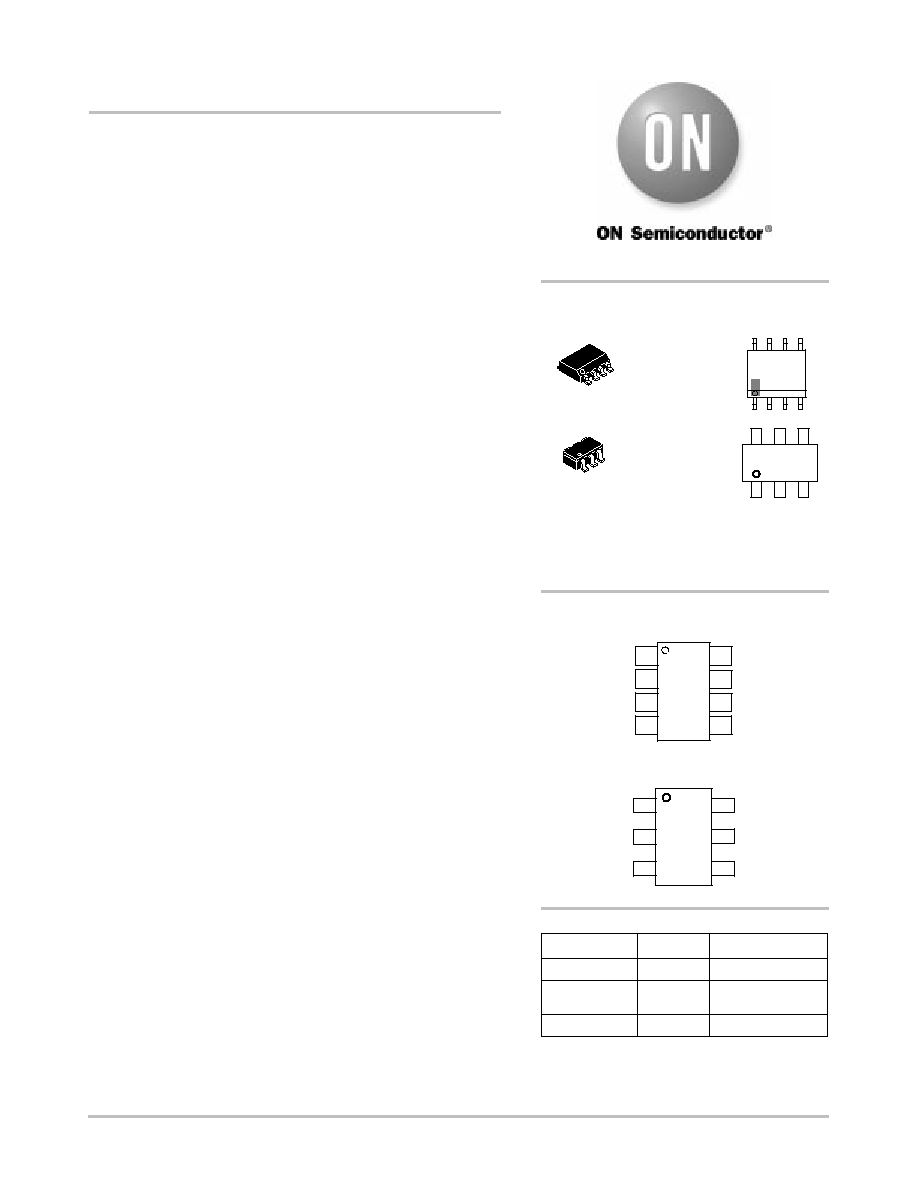
1
8
SOIC-8
D SUFFIX
CASE 751
1
8
5
3
4
(Top View)
FB
CS
NC
PIN CONNECTIONS
7
6
2
NC
CT
GND
Gate
V
CC
MARKING
DIAGRAMS
FAA
= Specific Device Code
A
= Assembly Location
L
= Wafer Lot
Y
= Year
W
= Work Week
1
6
TSOP-6
(SOT23-6, SC59-6)
SN SUFFIX
CASE 318G
FAAYW
1
6
SOIC-8
1
3
FB
CS
2
GND
CT
4
Gate
6
(Top View)
5
V
CC
TSOP-6
ORDERING INFORMATION
P1215
ALYW
Device
Package
Shipping
NCP1215DR2
SOIC-8
2500 Tape & Reel
NCP1215SNT1
TSOP-6
3000 Tape & Reel
For information on tape and reel specifications,
including part orientation and tape sizes, please
refer to our Tape and Reel Packaging Specifications
Brochure, BRD8011/D.
1
8
http://onsemi.com
NCP1215DR2G
SOIC-8
(Pb-Free)
2500 Tape & Reel
NCP1215
http://onsemi.com
2
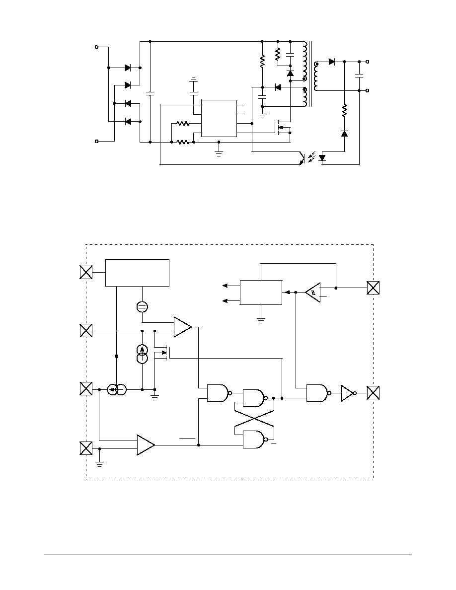
Figure 1. Typical Application
Line
Line
N
+
FB
GND
CT
CS
Gate
Vcc
NC
NC
+
+
+
-
*
* If your application requires a gate-source resistor, please refer to design guidelines in this document.
Figure 2. Representative Block Diagram
Feedback Loop
Control
-
+
FB
+
-
Off-Time
Comparator
CT
Voffset
0-7 V
10
m
A
12.5-50
m
A
CS
+
-
GND
Current Sense Comparator
Reset
Set
Q
Q
Reference
Regulator
V
DD
I
ref
-
+
Undervoltage
Lockout
12/8.5 V
Gate
V
CC
Gate Driver

NCP1215
http://onsemi.com
3
¡¡¡¡¡¡¡¡¡¡¡¡¡¡¡¡¡¡¡¡¡¡¡¡¡¡¡¡¡¡¡¡¡
¡
¡¡¡¡¡¡¡¡¡¡¡¡¡¡¡¡¡¡¡¡¡¡¡¡¡¡¡¡¡¡¡
¡
¡¡¡¡¡¡¡¡¡¡¡¡¡¡¡¡¡¡¡¡¡¡¡¡¡¡¡¡¡¡¡¡¡
PIN FUNCTION DESCRIPTION
¡¡¡¡
¡¡¡¡
TSOP-6
¡¡¡¡
¡¡¡¡
SOIC-8
¡¡¡¡¡¡
¡¡¡¡¡¡
Symbol
¡¡¡¡¡¡¡¡¡¡¡¡¡¡¡¡¡¡¡¡¡¡
¡¡¡¡¡¡¡¡¡¡¡¡¡¡¡¡¡¡¡¡¡¡
Description
4
1
FB
The FB pin provides voltage feedback loop. The current injected into the pin determines the
primary switch OFF time interval. It also influences the peak value of the primary current.
3
2
CT
Connection for an external timing programming capacitor.
1
3
CS
The CS pin senses the power switch current.
2
4
GND
Primary and internal ground.
6
5
Gate
Output drive for an external power MOSFET.
5
6
Vcc
Power supply voltage and Undervoltage Lockout.
7
7
NC
Unconnected pin.
8
8
NC
Unconnected pin.
¡¡¡¡¡¡¡¡¡¡¡¡¡¡¡¡¡¡¡¡¡¡¡¡¡¡¡¡¡¡¡¡¡
¡
¡¡¡¡¡¡¡¡¡¡¡¡¡¡¡¡¡¡¡¡¡¡¡¡¡¡¡¡¡¡¡
¡
¡¡¡¡¡¡¡¡¡¡¡¡¡¡¡¡¡¡¡¡¡¡¡¡¡¡¡¡¡¡¡¡¡
MAXIMUM RATINGS
¡¡¡¡¡¡¡¡¡¡¡¡¡¡¡¡¡¡¡¡¡¡
¡
¡¡¡¡¡¡¡¡¡¡¡¡¡¡¡¡¡¡¡¡
¡
¡¡¡¡¡¡¡¡¡¡¡¡¡¡¡¡¡¡¡¡¡¡
Rating
¡¡¡¡¡
¡
¡¡¡
¡
¡¡¡¡¡
Symbol
¡¡¡¡¡¡
¡
¡¡¡¡
¡
¡¡¡¡¡¡
Value
¡¡¡
¡
¡
¡
¡¡¡
Unit
Power Supply Voltage
V
cc
18
V
FB Pins Voltage Range
V
FB
-0.3 to 18
V
CS and CT Pin Voltage Range
V
in
-0.3 to 10
V
Thermal Resistance, Junction-to-Air (SOIC-8 Version)
R
q
JA
178
∞
C/W
Junction Temperature
T
J
150
∞
C
Storage Temperature Range
T
stg
-60 to +150
∞
C
ESD Voltage Protection, Human Body Model (Except CT Pin)
V
ESD-HBM
2.0
kV
ESD Voltage Protection, Human Body Model for CT Pin
V
ESD-HBM-CT
1.5
kV
ESD Voltage Protection, Machine Model (Except CT Pin)
V
ESD-MM
200
V
ESD Voltage Protection, Machine Model for CT Pin
V
ESD-MM-CT
150
V
Maximum ratings are those values beyond which device damage can occur. Maximum ratings applied to the device are individual stress limit
values (not normal operating conditions) and are not valid simultaneously. If these limits are exceeded, device functional operation is not implied,
damage may occur and reliability may be affected.

NCP1215
http://onsemi.com
4
ELECTRICAL CHARACTERISTICS
(V
CC
= 12 V, for typical values T
j
= 25
∞
C, for min/max values T
j
= 0
∞
C to +105
∞
C, unless
otherwise noted.)
Characteristic
Symbol
Min
Typ
Max
Unit
VOLTAGE FEEDBACK
Offset Voltage
V
offset
1.05
1.19
1.34
V
Maximum CT Pin Voltage at FB Current = 25
m
A (Including V
offset
)
V
CT-25
m
A
2.4
3.1
4.3
V
Maximum CT Pin Voltage at FB Current = 50
m
A (Including V
offset
)
V
CT-50
m
A
3.6
4.6
6.2
V
CT PIN - OFF TIME CONTROL
Source Current (CT Pin Grounded)
I
CT
8.0
9.8
11.5
m
A
Source Current Maximum Voltage Capability
V
CT-max
-
6.5
-
V
Minimum CT Pin Voltage (Pin Unloaded, Discharge Switch Turned On)
V
CT-min
-
-
20
mV
CURRENT SENSE
Minimum Source Current (I
FB
= 180
m
A, CT Pin Grounded)
I
CS-min
8.0
12.5
16
m
A
Maximum Source Current (I
FB
= 0
m
A, CT Pin Grounded)
I
CS-max
40
49
58
m
A
Comparator Threshold Voltage
V
th
15
42
80
mV
Propagation Delay (CS Falling Edge to Gate Output)
t
delay
-
215
310
ns
GATE DRIVE
Sink Resistance (I
sink
= 30 mA)
R
OL
25
40
90
W
Source Resistance (I
source
= 30 mA)
R
OH
60
80
130
W
POWER SUPPLY
V
CC
Startup Voltage
V
startup
-
12.5
14.2
V
Undervoltage Lockout Threshold Voltage
V
UVLO
7.2
9.0
-
V
Hysteresis (V
startup
- V
UVLO
)
V
hys
2.2
3.5
-
V
V
CC
Startup Current Consumption (V
CC
= 8.0 V)
I
CC-start
-
2.8
6.5
m
A
V
CC
Steady State Current Consumption
(C
GATE
= 1.0 nF, f
SW
= 100 kHz, FB open)
I
CC-SW
0.55
0.9
1.75
mA
NCP1215
http://onsemi.com
5
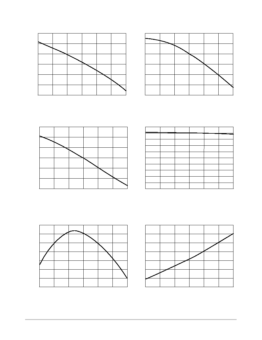
TYPICAL CHARACTERISTICS
-25
11.5
50
11.2
25
0
V
star
tup
, (V)
11.0
T
J
, JUNCTION TEMPERATURE (
∞
C)
11.6
T
J
, JUNCTION TEMPERATURE (
∞
C)
11.1
11.3
11.4
125
V
of
fset
, (V)
1.08
Figure 3. V
startup
Threshold vs. Junction
Temperature
Figure 4. V
UVLO
Threshold vs. Junction
Temperature
Figure 5. Operating Current Consumption vs.
Junction Temperature
Figure 6. Offset Voltage vs. Junction
Temperature
T
J
, JUNCTION TEMPERATURE (
∞
C)
Figure 7. Current Sense Source Current vs.
Junction Temperature
T
J
, JUNCTION TEMPERATURE (
∞
C)
Figure 8. Current Sense Threshold vs.
Junction Temperature
T
J
, JUNCTION TEMPERATURE (
∞
C)
1.12
1.00
1.16
1.20
75
100
-25
8.7
50
8.4
25
0
V
UVLO
, (V)
8.2
8.8
8.3
8.5
8.6
125
75
100
-25
0.985
50
0.970
25
0
I
CC-
SW
, (mA)
0.960
0.990
T
J
, JUNCTION TEMPERATURE (
∞
C)
0.965
0.975
0.980
125
75
100
-25
50
25
0
125
75
100
1.04
1.06
1.10
1.14
1.18
1.02
-25
48.0
50
46.5
25
0
I
CS-
m
ax
, (
m
A)
45.5
49.0
46.0
47.0
47.5
125
75
100
48.5
-25
55
50
40
25
0
V
CS-
t
h
, (mV)
30
65
35
45
50
125
75
100
60
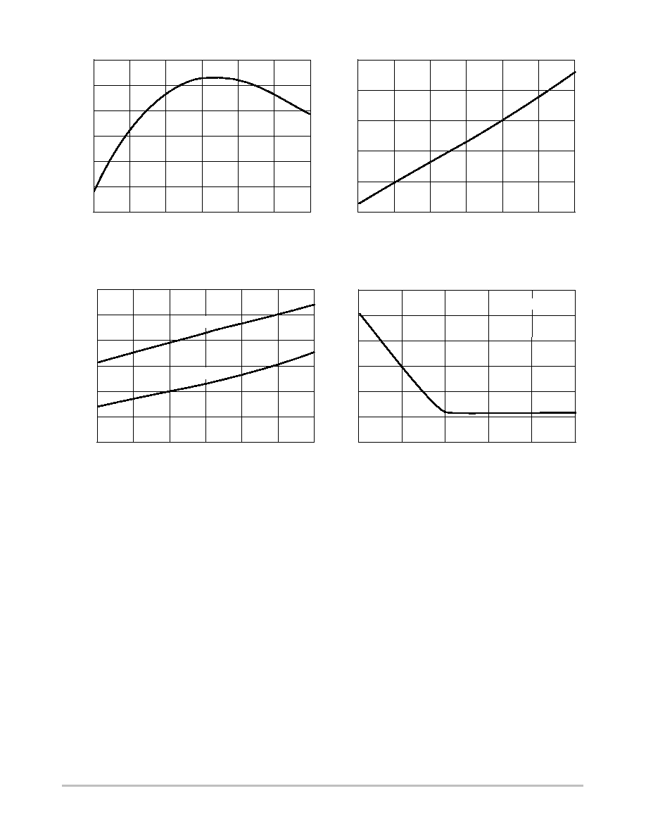
NCP1215
http://onsemi.com
6
-25
9.9
50
9.6
25
0
I
CT
, (
m
A)
9.4
T
J
, JUNCTION TEMPERATURE (
∞
C)
10.0
T
J
, JUNCTION TEMPERATURE (
∞
C)
9.5
9.7
9.8
125
I
CS
, (
m
A)
40.0
Figure 9. CT pin Source Current vs. Junction
Temperature
Figure 10. CT pin Threshold vs. Junction
Temperature
Figure 11. Drive Sink and Source Resistance
vs. Junction Temperature
Figure 12. Current Sense Source Current vs.
Feedback Current
I
fb
, FEEDBACK CURRENT (
m
A)
60.0
0.0
75
100
-25
50
10
25
0
V
CT-
m
in
, (mV)
6
16
8
12
14
125
75
100
-25
100
50
40
25
0
R
source
-R
sink,
(
W
)
0
120
T
J
, JUNCTION TEMPERATURE (
∞
C)
20
60
80
125
75
100
50
25
0
125
75
100
20.0
30.0
50.0
10.0
R
source
R
sink
T
J
= 25
∞
C
NCP1215
http://onsemi.com
7
APPLICATION INFORMATION
The NCP1215 implements a current mode SMPS with a
variable OFF-time dependant upon output power demand.
It can be seen from the typical application that NCP1215 is
designed to operate with a minimum number of external
component. The NCP1215 incorporates the following
features:
∑
Frequency Foldback: Since the switch-off time
increases when power demand decreases, the switching
frequency naturally diminishes in light load conditions.
This helps to minimize switching losses and offers
excellent standby power performance.
∑
Very Low Startup Current: The patented internal
supply block is specially designed to offer a very low
current consumption during startup. It allows the use of
a very high value external startup resistor, greatly
reducing dissipation, improving efficiency and
minimizing standby power consumption.
∑
Natural Frequency Dithering: The quasi-fixed T
on
mode of operation improves the EMI signature since
the switching frequency varies with the natural bulk
ripple voltage.
∑
Peak Current Compression: As the load becomes
lighter, the frequency decreases and can enter the
audible range. To avoid exciting transformer
mechanical resonances, hence generating acoustic
noise, the NCP1215 includes a patented technique,
which reduces the peak current as power goes down.
As such, inexpensive transformer can be used without
having noise problems.
∑
Negative Primary Current Sensing: By sensing
the total current, this technique does not modify the
MOSFET driving voltage (Vgs) while switching.
Furthermore, the programming resistor together with the
pin capacitance, forms a residual noise filter which
blanks spurious spikes. Also fixing primary current level
to a maximum value sets the maximum power limit.
∑
Programmable Primary Current Sense: It offers a
second peak current adjustment variable which improves
the design flexibility.
∑
Secondary or Primary Regulation: The feedback
loop arrangement allows simple secondary or primary
side regulation without significant additional external
components.
A detailed description of each internal block within the IC
is given in the following.
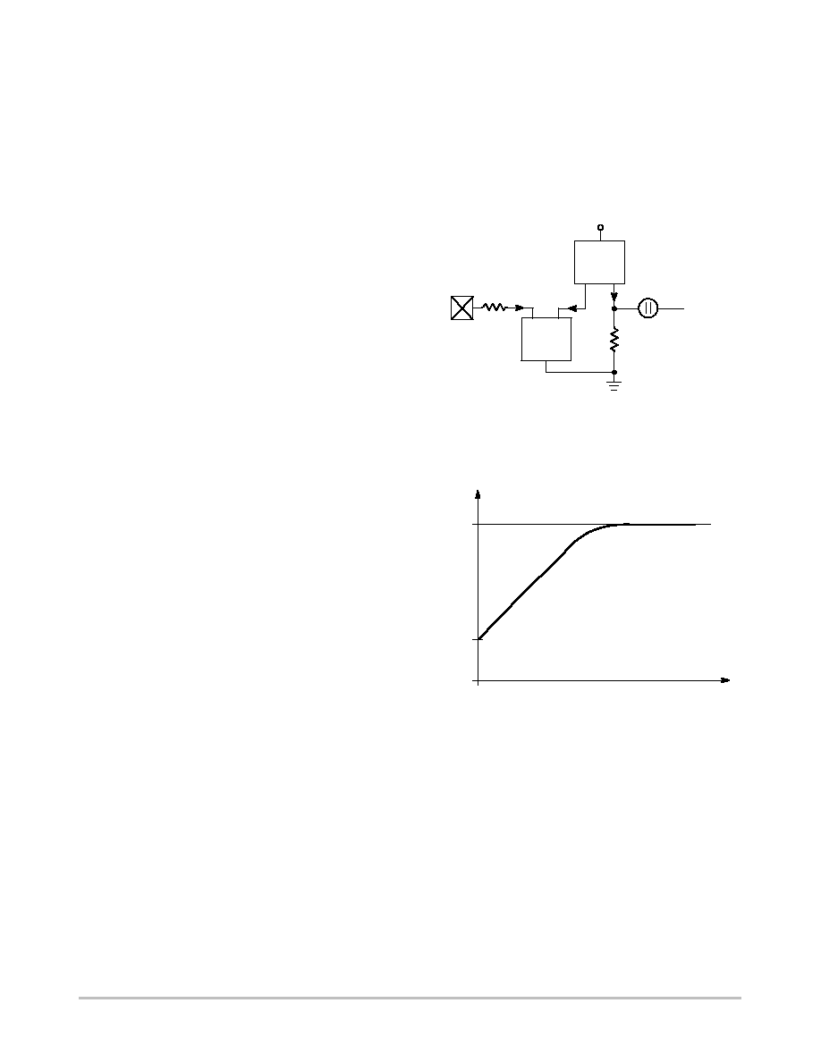
Feedback Loop Control
The main task of the Feedback Loop Block is to control
the SMPS output voltage through the change of primary
switch OFF time interval. It sets the peak voltage of the
timing capacitor, which varies upon the output power
demand. Figure 13 shows the simplified internal schematic:
Figure 13. Feedback Loop - OFF Time Control
FB
17 k
Current
Mirror
1:1
Current
Mirror
1:1
-
+
To OFF
Time
Comparator
45 k
V
offset
V
CC
The voltage feedback signal is sensed as a current injected
through the FB pin.
Figure 14. FB Loop Transfer Characteristic
OFF-T
ime
Comparator Input V
oltage
V
DD
V
offset
0
m
A
FB Pin Sink Current
The transfer characteristic (output voltage to input
current) of the feedback loop control block can be seen in
Figure 14. V
DD
refers to the internal stabilized supply
whereas the offset value sets the maximum switching
frequency in lack of optocoupler current (e.g. an output
short-circuit).
To keep the switching frequency above the audio range in
light load condition the FB pin also regulates in certain range
the peak primary current. The corresponding block diagram
can be seen from Figure 15.
NCP1215
http://onsemi.com
8
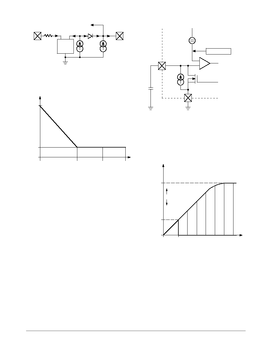
Figure 15. Feedback Loop - Current Sense Control
FB
17 k
Current
Mirror
4:3
37.5
m
A
12.5
m
A
CS
To Current Sense Comparator
The resulting current sense regulation characteristic can
be seen from Figure 16.
Figure 16. Current Sense Regulation Characteristic
CS Pin Source Current
12.5
m
A
50
m
A
140
m
A
100
m
A
50
m
A
0
m
A
FB Pin Sink Current
When the load goes light, the compression circuitry
decreases the peak current. This has the effect of slightly
increasing the switching frequency but the compression
ratio is selected to not hamper the standby power.
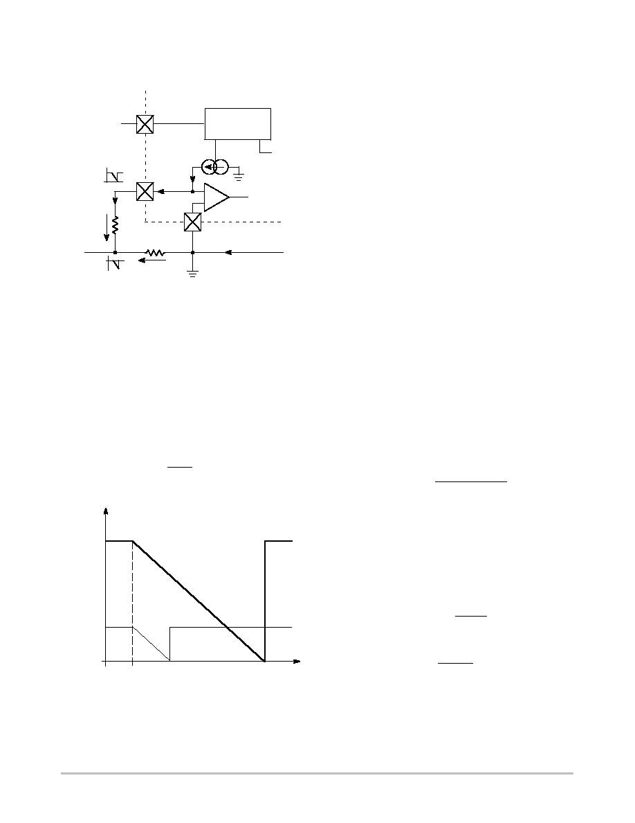
OFF Time Control
The loop signal together with the internal current source,
via an external capacitor, controls the switch-off time. This
is portrayed in Figure 17.
Figure 17. OFF Time Control
-
+
+
-
CT
Voffset
10
m
A
From Feedback Loop Block
V
offset
to V
DD
To Latch's Set Input
To Latch's Output
GND
CT
During the switch-ON time, the CT capacitor is kept
discharged by a MOSFET switch. As soon as the latch
output changes to a low state, the voltage across CT created
by the internal current source, starts to ramp-up until its
value reaches the threshold given by the feedback loop
demand.
Figure 18. CT
Pin Voltage (P
out
1
u
P
out
2
u
P
out
3)
V
offset
V
DD
V
CT Pin
Voltage
P
OUT
Goes Down
P
OUT
Goes Up
t
off-min
t
P3
P2
P1
The voltage that can be observed on CT pin is shown in
Figure 18. The bold waveform shows the maximum output
power when the OFF time is at its minimum. The IC allows
an OFF time of several seconds.
NCP1215
http://onsemi.com
9
Primary Current Sensing
The primary current sensing circuit is shown in Figure 19.
CS
R
shift
V
shift
R
CS
V
CS
GND
+
-
To Latch
I
primary
Figure 19. Primary Current Sensing
12.5
m
A
B
50
m
A
Feedback Loop
Control
FB
When the primary switch is ON, the transformer current
flows through the sense resistor R
cs
. The current creates a
voltage, V
cs
which is negative with respect to GND. Since
the comparator connected to CS pin requires a positive
voltage, the voltage V
shift
is developed across the resistor
R
shift
by a current source which level-shifts the negative
voltage V
cs
. The level-shift current is in range from 12.5 to
50
mA depending on the Feedback Loop Control block
signal (see more details in the Feedback Loop Control
section).
The peak primary current is thus equal to:
Ipk
+
Rshift
RCS
∑ ICS
(eq. 1)
A typical CS pin voltage waveform is shown in Figure 20.
Figure 20. CS Pin Voltage
0
t
Switch
Turn-on
I
shift
= 12.5
m
A
I
shift
= 50
m
A
V
Figure 20 also shows the effect of the inductor current of
differing output power demand.
The primary current sensing method we described, brings
the following benefits compared to the traditional approach:
∑
Maximum peak voltage across the current sense resistor
is determined and can be optimized by the value of the
shift resistor.
∑
CS pin is not exposed to negative voltage, which could
induce a parasitic substrate current within the IC and
distort the surrounding internal circuitry.
∑
The gate drive capability is improved because the
current sense resistor is located out of the gate driver
loop and does not deteriorate the turn-on and also
turn-off gate drive amplitude.
Gate Driver
The Gate Driver consists of a CMOS buffer designed to
directly drive a power MOSFET.
It features an unbalanced source and sink capabilities to
optimize turn ON and OFF performance without additional
external components. Since the power MOSFET turns-off
at high drain current, to minimize its turn-off losses the sink
capability of the gate driver is increased for a faster turn-off.
To the opposite, the source capability is lower to slow-down
power MOSFET at turn-on in order to reduce the EMI noise.
Whenever the IC supply voltage is lower than the
undervoltage threshold, the Gate Driver is low, pulling down
the gate to ground. It eliminates the need for an external
resistor.
Startup Circuit
An external startup resistor is connected between high
voltage potential of the input bulk capacitor and Vcc supply
capacitor. The value of the resistor can be calculated as
follows:
Rstartup
+
Vbulk
*
Vstartup
Istartup
(eq. 2)
Where:
V
startup
V
cc
voltage at which IC starts operation
(see spec.)
I
startup
Startup current
V
bulk
Input bulk capacitor's voltage
Since the V
bulk
voltage has obviously much higher value
than V
startup
the equation can be simplified in the following
way:
Rstartup
+
Vbulk
Istartup
(eq. 3)
The startup current can be calculated as follows:
Istartup
+
CVcc
Vstartup
tstartup
)
ICC-start
(eq. 4)
Where:
C
Vcc
Vcc capacitor value
t
startup
Startup time
I
CC-start
IC current consumption (see spec.)

NCP1215
http://onsemi.com
10
If the IC current consumption is assumed constant during
the startup phase, one can obtain resulting equation for
startup resistor calculation:
Rstartup
+
Vbulk
CVcc
Vstartup
tstartup
)
ICC-start
(eq. 5)
Switching Frequency
The switching frequency varies with the output load and
input voltage. The highest frequency appears at highest
input voltage and maximum output power.
Since the peak primary current is fixed, the on time
portion of the switching period can be calculated:
ton
+
Lp
Ipk
Vbulk
(eq. 6)
Where:
L
p
Transformer primary inductance
I
pk
Peak primary current
Using equation for peak primary current estimation the
switch-on time is:
ton
+
Lp
Rshift
Rcs ∑ Vbulk
50 ∑ 10-6
(eq. 7)
Minimum switch-on time occurs at maximum input
voltage:
ton- min
+
Lp
Rshift
Rcs ∑ Vbulk- max
50 ∑ 10-6
(eq. 8)
As it can be seen from the above equation, the switch-on
time linearly depends on the input bulk capacitor voltage.
Since this voltage has ripple due to AC input voltage and
input rectifier, it allows natural frequency dithering to
improve EMI signature of the SMPS.
The switch-off time is determined by the charge of an
external capacitor connected to the CT pin. The minimum
Toff value can be computed by:
toff- min
+
CT
Voffset
ICt
+
CT
1.2
10-5
(eq. 9)
+
0.12 ∑ 106 CT
Where:
V
offset
Offset voltage (see spec.)
I
Ct
CT pin source current (see spec.)
The maximum switching frequency then can be evaluated
by:
(eq. 10)
fsw- max
+
1
ton- min
)
toff- min
+
1
Lp ∑ Rshift
Vbulk ∑ Rcs
∑ 50 ∑ 10-6
)
0.12 ∑ 106 ∑ CT
As output power diminishes, the switching frequency
decreases because the switch-off time prolongs upon
feedback loop. The range of the frequency change is
sufficient to keep output voltage regulation in any light load
condition.
Application Design Example
An example of the typical wall adapter application is
described hereafter.
As a wall adapter it should be able to operate properly with
wide range of the input voltage from 90 VAC up to 265 VAC.
The bulk capacitor voltage then can be calculated:
(eq. 11)
Vbulk- min
+
VAC- min 2
+
90 ∑
2
+
127 VDC
(eq. 12)
Vbulk- max
+
VAC- max 2
+
265 ∑
2
+
375 VDC
The requested output power is 5.2 Watts.
Assuming 80% efficiency the input power is equal to:
(eq. 13)
Pin
+
Pout
h +
5.2
0.8
+
6.5 W
The average value of input current at minimum input
voltage is:
(eq. 14)
Iin-avg
+
Pin
Vbulk- min
+
6.5
127
+
51.2 mA
The suitable reflected primary winding voltage for 600 V
rated MOSFET switch is:
(eq. 15)
Vflbk
+
600 V
*
Vbulk- max
*
Vspike
+
600
*
375
*
100
+
125 V
Using calculated flyback voltage the maximum duty cycle
can be calculated:
(eq. 16)
d
max
+
Vflbk
Vflbk
)
Vbulk- min
+
125
125
)
127
+
0.496
+
0.5
Following equation determines peak primary current:
(eq. 17)
Ippk
+
2 ∑ Iin-avg
d
max
+
2 ∑ 51.2 ∑ 10-3
0.5
+
204.7 mA
The desired maximum switching frequency at minimum
input voltage is 75 kHz.
The highest switching frequency occurs at the highest
input voltage and its value can be estimated as follows:
(eq. 18)
f max -high
+
f max -low
Vbulk- max
Vbulk- min
d
max
+
75 ∑ 103
375
127
0.5
+
110.7 kHz
This frequency is much below 150 kHz, so that the desired
operating frequency can be exploited for further calculation
of the primary inductance:
(eq. 19)
Lp
+
Vbulk- min ∑
d
max
Ippk ∑ fsw- max
+
127 ∑ 0.5
0.2047 ∑ 75 ∑ 103
+
4.14 mH

NCP1215
http://onsemi.com
11
The EF16 core for transformer was selected. It has
cross-section area A
e
= 20.1 mm
2
. The N67 magnetic
allows to use maximum operating flux density
B
max
= 0.28 Tesla.
The number of turns of the primary winding is:
(eq. 20)
np
+
Lp ∑ Ippk
B max ∑ Ae
+
4.14 ∑ 10-3 ∑ 0.2047
0.28 ∑ 20.1 ∑ 10-6
+
150 turns
The A
L
factor of the transformer's core can be calculated:
(eq. 21)
AL
+
Lp
(np)2
+
4.14 ∑ 10-3 ∑
(150)2
+
184 nH
For an adapter output voltage of 6.5 V, the number of turns
of the secondary winding can be calculated accounting
Schottky diode for output rectifier as follows:
(eq. 22)
ns
+
(Vs
)
Vfwd)(1
* d
max)np
d
max ∑ Vbulk- min
+
(6.5
)
0.7)(1
*
0.5)150
0.5 ∑ 127
+
8.5
+
9 turns
The number of turns for auxiliary winding can be
calculated similarly:
(eq. 23)
ns
+
(Vs
)
Vfwd)(1
* d
max)np
d
max ∑ Vbulk- min
+
(12
)
1)(1
*
0.5)150
0.5 ∑ 127
+
15.35
+
15 turns
The peak primary current is known from initial
calculations. The current sense method allows choosing the
voltage drop across the current sense resistor. Let's use a
value of 0.5 V. The value of the current sense resistor can
then be evaluated as follows:
(eq. 24)
RCS
+
VCS
Ippk
+
0.5
0.2047
+
2.442
W +
2.7
W
The voltage drop across the sense resistor needs to be
recalculated:
(eq. 25)
VCS
+
RCS ∑ Ippk
+
2.7 ∑ 0.2047
+
0.553 V
Using the above results the value of the shift resistor is:
(eq. 26)
Rshift
+
VCS
ICS
+
0.553
50 ∑ 10-6
+
11.06 k
W +
11 k
W
The value of timing capacitor for the off time control has
to be calculated for minimum bulk capacitor voltage since
at these conditions the converter should be able to deliver
specified maximum output power. The value of the timing
capacitor is then given by the following equation:
(eq. 27)
CT
+
1
fsw
*
Lp ∑ Ippk
Vbulk- min
1.2 ∑ 106
+
1
75 ∑ 103
*
4.14 ∑ 10
*
3 ∑ 0.2047
127
0.12 ∑ 106
+
55.5 pF
+
56 pF
The value of the startup resistor for startup time of 200 ms
and Vcc capacitor of 200 nF is following:
(eq. 28)
Rstartup
+
Vbulk- min
CVcc
Vstartup
tstartup
)
ICC-start MAX
+
127
200 ∑ 10-9
12
0.2
)
10 ∑ 10-6
+
5.77 M
W +
5.6 M
W
The result of all the calculations is the application
schematic depicted in Figure 21.
NCP1215
http://onsemi.com
12
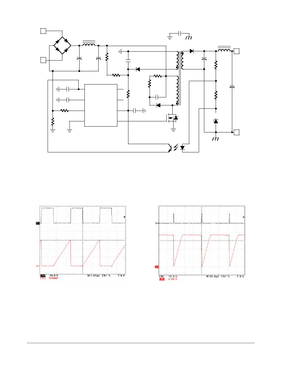
Figure 21. Adaptor Application Schematic
Line
J1
1
S250
3 D1
Neutral
J2
1
4
2
2.2
m
F/
400 V
C1
+
+ 1
L1
2.2 mH
2.2
m
F/
400 V
C2
+
R3
2M7
R4
2M7
C5
100 nF
D5
LL4448
IC1
GND
CS
CT
FB
10 nF
4
3
2
1
C3
C4
56 pF
11 k R2
R1
2.7
NCP1215
Gate
V
CC
NC2
NC1
X
X
5
6
7
8
R5
220
C6
100 nF
R7
47 k
R6
47 k
1 nF/
500 V
C7
D8
MURA160T3
MTD1N60
Q1
1
2
3
4
5
8
D9 MBRS360T3
J3
1
+6.5 V@
800 mA
L2
4.7
m
H
+
C9
470
m
F/
16 V
R8
220
10
m
F/
16 V +
C10
BZX84C5V6
R9
1 k
D7
J4
1
GND
ISO1
PC817
-
T1
C8
1 nF/Y
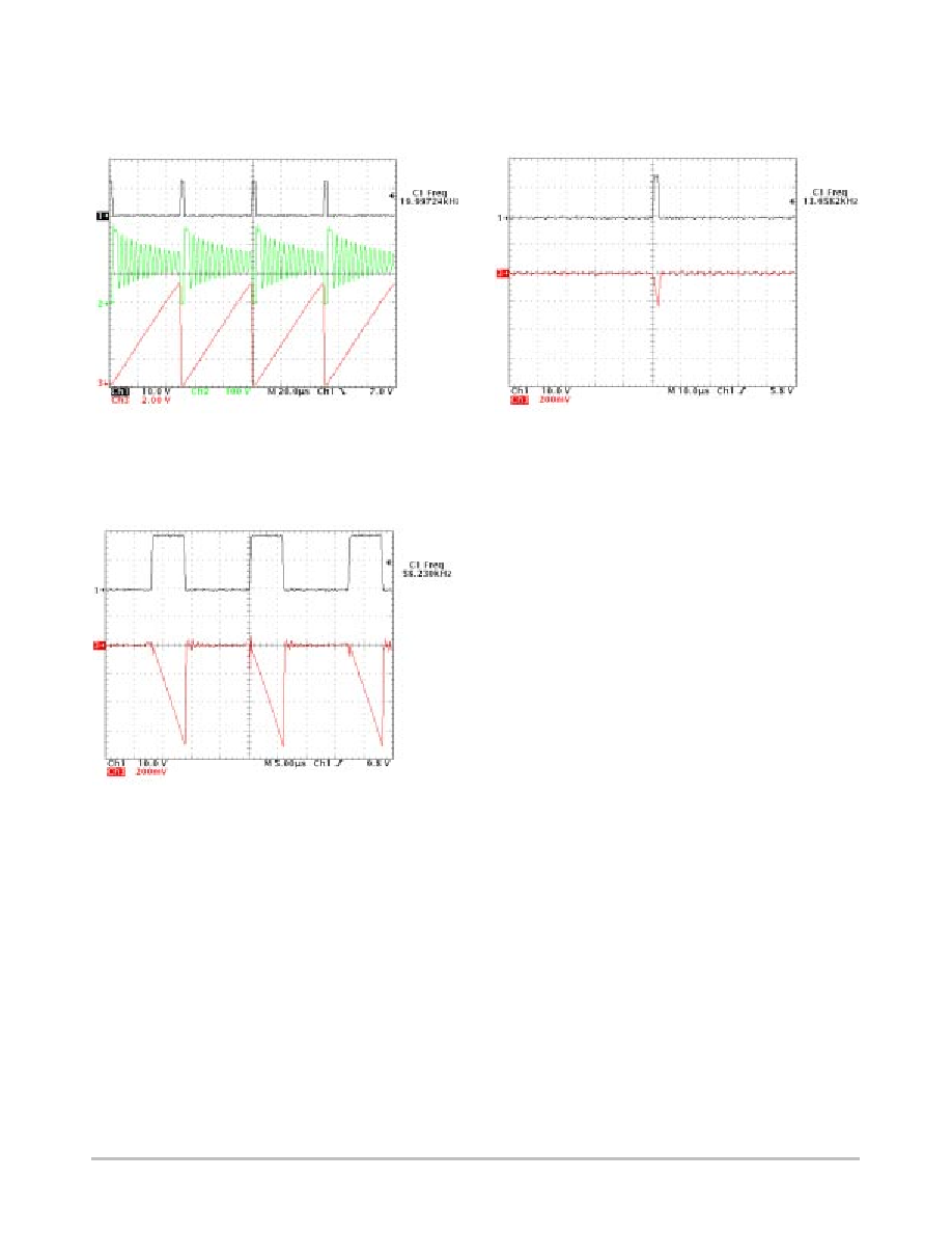
The following oscilloscope snapshots illustrate the
operation of the working adapter. The Channel 3 in
Figure 22 shows CT pin voltage at full output load. The
Channel 1 is a gate driver output.
The CT voltage at no load condition is depicted in
Figure 23.
Figure 22. CT Voltage at Full Load Condition
Figure 23. CT Voltage at No Load Condition
NCP1215
http://onsemi.com
13
Figure 24 shows CT voltage and also by Channel 2 the
switch's drain voltage at light load conditions.
Figure 24. CT and Drain at Light Load
The waveform on the current sense pin at full load
conditions can be observed from Channel 3 in Figure 25.
Figure 25. CS Pin at Full Load Condition
Figure 26 demonstrates the reduction of the peak primary
current at light load conditions.
Figure 26. CS Pin at Light Load Condition
Gate-Source Resistor Design Guidelines
In some applications, there is a need to wire a resistor
between the MOSFET gate and source connections. This
can preclude an eventual MOSFET destruction if, in the
production stage, the converter is powered whilst the gate is
left unconnected. However, dealing with an extremely low
startup current implies a careful selection of the gate-source
resistance. With the NCP1215, the gate-source resistor must
be calculated to allow the growth of the V
CC
capacitor to
4.0 V in order to not interfere with the power-on sequence.
The following equation helps deriving Rgate-source,
accounting for the minimum rectified input voltage and the
startup resistor: Vin
min
x Rgate-source/(Rgate-source +
Rstartup)
u 4.0 V. If we take a Vin
min
of 100 VDC, a startup
resistor of 4.0 M
W, then Rgate-source equals 180 kW as a
minimum normalized value.
NCP1215
http://onsemi.com
14
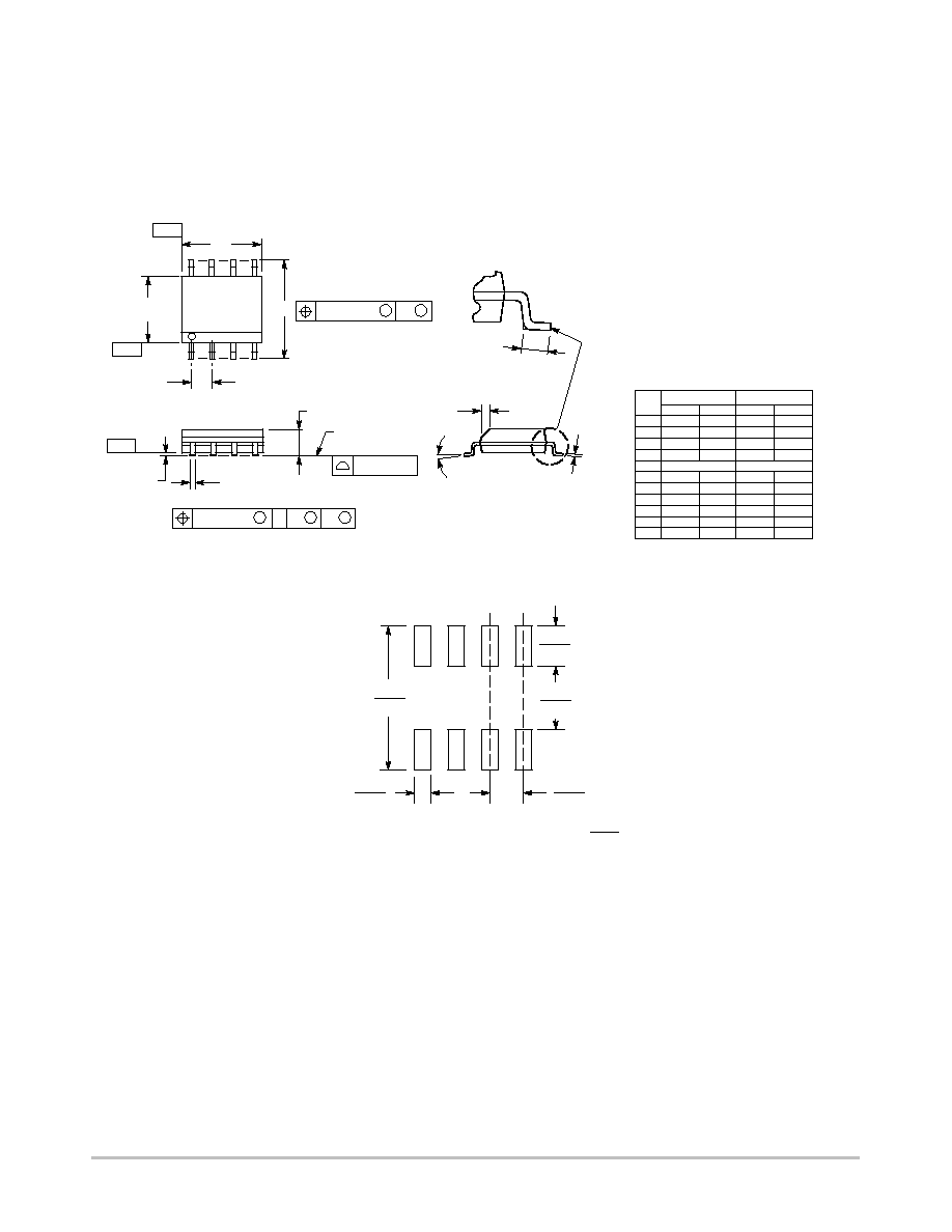
PACKAGE DIMENSIONS
SOIC-8
D SUFFIX
CASE 751-07
ISSUE AC
*For additional information on our Pb-Free strategy and soldering
details, please download the ON Semiconductor Soldering and
Mounting Techniques Reference Manual, SOLDERRM/D.
SOLDERING FOOTPRINT*
SEATING
PLANE
1
4
5
8
N
J
X 45
_
K
NOTES:
1. DIMENSIONING AND TOLERANCING PER
ANSI Y14.5M, 1982.
2. CONTROLLING DIMENSION: MILLIMETER.
3. DIMENSION A AND B DO NOT INCLUDE
MOLD PROTRUSION.
4. MAXIMUM MOLD PROTRUSION 0.15 (0.006)
PER SIDE.
5. DIMENSION D DOES NOT INCLUDE DAMBAR
PROTRUSION. ALLOWABLE DAMBAR
PROTRUSION SHALL BE 0.127 (0.005) TOTAL
IN EXCESS OF THE D DIMENSION AT
MAXIMUM MATERIAL CONDITION.
6. 751-01 THRU 751-06 ARE OBSOLETE. NEW
STANDARD IS 751-07.
A
B
S
D
H
C
0.10 (0.004)
DIM
A
MIN
MAX
MIN
MAX
INCHES
4.80
5.00
0.189
0.197
MILLIMETERS
B
3.80
4.00
0.150
0.157
C
1.35
1.75
0.053
0.069
D
0.33
0.51
0.013
0.020
G
1.27 BSC
0.050 BSC
H
0.10
0.25
0.004
0.010
J
0.19
0.25
0.007
0.010
K
0.40
1.27
0.016
0.050
M
0
8
0
8
N
0.25
0.50
0.010
0.020
S
5.80
6.20
0.228
0.244
-X-
-Y-
G
M
Y
M
0.25 (0.010)
-Z-
Y
M
0.25 (0.010)
Z
S
X
S
M
_
_
_
_
1.52
0.060
7.0
0.275
0.6
0.024
1.270
0.050
4.0
0.155
mm
inches
SCALE 6:1
NCP1215
http://onsemi.com
15
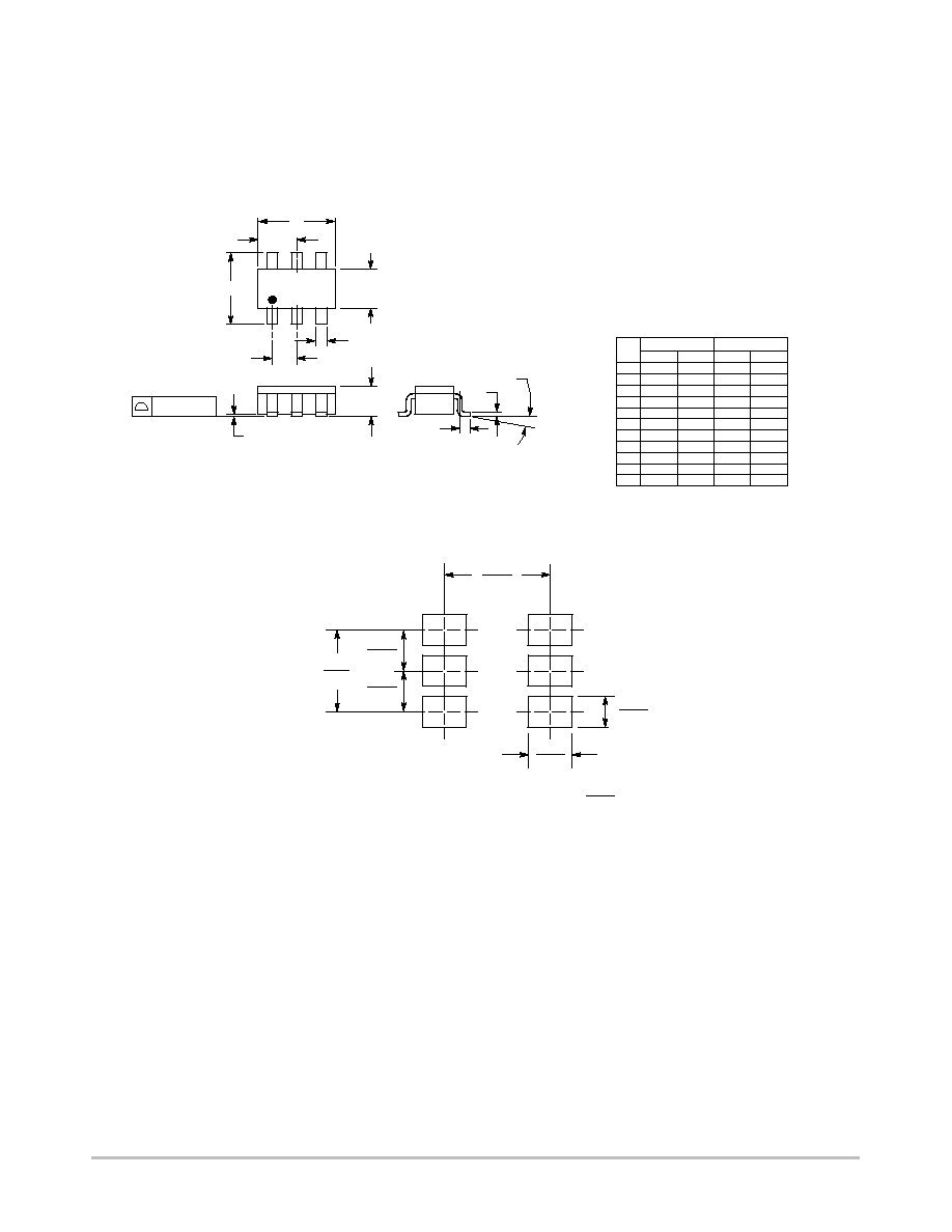
PACKAGE DIMENSIONS
TSOP-6
CASE 318G-02
ISSUE M
0.95
0.037
1.9
0.075
0.95
0.037
mm
inches
SCALE 10:1
1.0
0.039
2.4
0.094
0.7
0.028
2
3
4
5
6
A
L
1
S
G
D
B
H
C
0.05 (0.002)
DIM
MIN
MAX
MIN
MAX
INCHES
MILLIMETERS
A
0.1142 0.1220
2.90
3.10
B
0.0512 0.0669
1.30
1.70
C
0.0354 0.0433
0.90
1.10
D
0.0098 0.0197
0.25
0.50
G
0.0335 0.0413
0.85
1.05
H
0.0005 0.0040
0.013
0.100
J
0.0040 0.0102
0.10
0.26
K
0.0079 0.0236
0.20
0.60
L
0.0493 0.0610
1.25
1.55
M
0
10
0
10
S
0.0985 0.1181
2.50
3.00
_
_
_
_
NOTES:
1. DIMENSIONING AND TOLERANCING PER
ANSI Y14.5M, 1982.
2. CONTROLLING DIMENSION: MILLIMETER.
3. MAXIMUM LEAD THICKNESS INCLUDES
LEAD FINISH THICKNESS. MINIMUM LEAD
THICKNESS IS THE MINIMUM THICKNESS
OF BASE MATERIAL.
4. DIMENSIONS A AND B DO NOT INCLUDE
MOLD FLASH, PROTRUSIONS, OR GATE
BURRS.
M
J
K
*For additional information on our Pb-Free strategy and soldering
details, please download the ON Semiconductor Soldering and
Mounting Techniques Reference Manual, SOLDERRM/D.
SOLDERING FOOTPRINT*

NCP1215
http://onsemi.com
16
ON Semiconductor and are registered trademarks of Semiconductor Components Industries, LLC (SCILLC). SCILLC reserves the right to make changes without further notice
to any products herein. SCILLC makes no warranty, representation or guarantee regarding the suitability of its products for any particular purpose, nor does SCILLC assume any liability
arising out of the application or use of any product or circuit, and specifically disclaims any and all liability, including without limitation special, consequential or incidental damages.
"Typical" parameters which may be provided in SCILLC data sheets and/or specifications can and do vary in different applications and actual performance may vary over time. All
operating parameters, including "Typicals" must be validated for each customer application by customer's technical experts. SCILLC does not convey any license under its patent rights
nor the rights of others. SCILLC products are not designed, intended, or authorized for use as components in systems intended for surgical implant into the body, or other applications
intended to support or sustain life, or for any other application in which the failure of the SCILLC product could create a situation where personal injury or death may occur. Should
Buyer purchase or use SCILLC products for any such unintended or unauthorized application, Buyer shall indemnify and hold SCILLC and its officers, employees, subsidiaries, affiliates,
and distributors harmless against all claims, costs, damages, and expenses, and reasonable attorney fees arising out of, directly or indirectly, any claim of personal injury or death
associated with such unintended or unauthorized use, even if such claim alleges that SCILLC was negligent regarding the design or manufacture of the part. SCILLC is an Equal
Opportunity/Affirmative Action Employer. This literature is subject to all applicable copyright laws and is not for resale in any manner.
PUBLICATION ORDERING INFORMATION
N. American Technical Support: 800-282-9855 Toll Free
USA/Canada
Japan: ON Semiconductor, Japan Customer Focus Center
2-9-1 Kamimeguro, Meguro-ku, Tokyo, Japan 153-0051
Phone: 81-3-5773-3850
NCP1215/D
The product described herein (NCP1215), may be covered by the following U.S. patents: 6,385,060, 6,605,978. There may be other patents pending.
LITERATURE FULFILLMENT:
Literature Distribution Center for ON Semiconductor
P.O. Box 61312, Phoenix, Arizona 85082-1312 USA
Phone: 480-829-7710 or 800-344-3860 Toll Free USA/Canada
Fax: 480-829-7709 or 800-344-3867 Toll Free USA/Canada
Email: orderlit@onsemi.com
ON Semiconductor Website: http://onsemi.com
Order Literature: http://www.onsemi.com/litorder
For additional information, please contact your
local Sales Representative.