
©
Semiconductor Components Industries, LLC, 2003
July, 2003 - Rev. 1
1
Publication Order Number:
NCP1216/D
NCP1216
PWM Current-Mode
Controller for High-Power
Universal Off-line Supplies
Housed in a SO-8 or DIP7 package, the NCP1216 represents an
enhanced version of NCP1200-based controllers. Due to its high drive
capability, NCP1216 drives large gate-charge MOSFETs, which
together with internal ramp compensation and built-in frequency
jittering, ease the design of modern AC/DC adapters.
With an internal structure operating at different fixed frequencies,
the controller supplies itself from the high-voltage rail, avoiding the
need of an auxiliary winding. This feature naturally eases the designer
task in some particular applications, e.g. battery chargers or TV sets.
C u r re nt -mod e co n trol a ls o p r ov i de s an excell en t input
audio-susceptibility and inherent pulse-by-pulse control. Internal
ramp compensation easily prevents sub-harmonic oscillations from
taking place in continuous conduction mode designs.
When the current setpoint falls below a given value, e.g. the output
power demand diminishes, the IC automatically enters the so-called
skip cycle mode and provides excellent efficiency at light loads.
Because this occurs at a user adjustable low peak current, no acoustic
noise takes place.
The NCP1216 features an efficient protective circuitry, which in
presence of an over current condition disables the output pulses while
the device enters a safe burst mode, trying to re-start. Once the default
has gone, the device auto-recovers.
Features
∑
No Auxiliary Winding Operation
∑
Current-Mode Control with Adjustable Skip-Cycle Capability
∑
Internal Ramp Compensation
∑
Built-In Frequency Jittering for Better EMI Signature
∑
Auto-Recovery Internal Output Short-Circuit Protection
∑
Extremely Low No-Load Stand-By Power
∑
500 mA Peak Current Capability
∑
Fixed Frequency Versions at 65 kHz, 100 kHz, 133 kHz
∑
Internal Temperature Shutdown
∑
Direct Optocoupler Connection
∑
SPICE Models Available for TRANsient and AC Analysis
∑
Pin-to-Pin Compatible with NCP1200 Series
Typical Applications
∑
High Power AC/DC Converters for TVs, Set-Top Boxes, etc.
∑
Offline Adapters for Notebooks
∑
Telecom DC-DC Converters
∑
All Power Supplies
This document contains information on a product under development. ON Semiconductor
reserves the right to change or discontinue this product without notice.
http://onsemi.com
SO-8
D SUFFIX
CASE 751
MINIATURE PWM
CONTROLLER FOR HIGH
POWER AC/DC WALL
ADAPTERS AND OFFLINE
BATTERY CHARGERS
MARKING
DIAGRAMS
16Dyy
ALYW
1
8
PDIP-7
P SUFFIX
CASE 626B
P1216Pxxx
AWL
YYWW
1
xxx
= Specific Device Code: 065, 100 or 133
yy
= Specific Device Code
(06 for 65, 10 for 100, 13 for 133)
A
= Assembly Location
WL, L
= Wafer Lot
YY, Y
= Year
WW, W = Work Week
PIN CONNECTIONS
1
Adj
8 HV
2
FB
3
CS
4
Gnd
7 NC
6 V
CC
5 Drv
See detailed ordering and shipping information in the package
dimensions section on page 15 of this data sheet.
ORDERING INFORMATION

NCP1216
http://onsemi.com
2
Universal Input
Fosc = 35kHz
HV
Vcc
Drv
GND
Adj
FB
CS
NCP1216
EMI
Filter
1
2
3
4
5
6
7
8
R
sense
R
comp
+
+
+
*See Application Section
Figure 1. Typical Application Example
¡¡¡¡¡¡¡¡¡¡¡¡¡¡¡¡¡¡¡¡¡¡¡¡¡¡¡¡¡¡¡¡¡
¡
¡¡¡¡¡¡¡¡¡¡¡¡¡¡¡¡¡¡¡¡¡¡¡¡¡¡¡¡¡¡¡
¡
¡¡¡¡¡¡¡¡¡¡¡¡¡¡¡¡¡¡¡¡¡¡¡¡¡¡¡¡¡¡¡¡¡
PIN FUNCTION DESCRIPTION
Pin No.
Pin Name
Function
Pin Description
1
Adj
Adjust the Skipping Peak Current
This pin lets you adjust the level at which the cycle skipping
process takes place. Shorting this pin to ground, permanently
disables the skip cycle feature.
2
FB
Sets the Peak Current Setpoint
By connecting an Optocoupler to this pin, the peak current set-
point is adjusted accordingly to the output power demand.
3
CS
Current Sense Input
This pin senses the primary current and routes it to the internal
comparator via an L.E.B. By inserting a resistor in series with the
pin, you control the amount of ramp compensation you need.
4
GND
IC Ground
-
5
Drv
Driving Pulses
The driver's output to an external MOSFET.
6
V
CC
Supplies the IC
This pin is connected to an external bulk capacitor of typically
22
m
F.
7
NC
-
This un-connected pin ensures adequate creepage distance.
8
HV
Generates the V
CC
from the Line
Connected to the high-voltage rail, this pin injects a constant
current into the V
CC
bulk capacitor.
NCP1216
http://onsemi.com
3
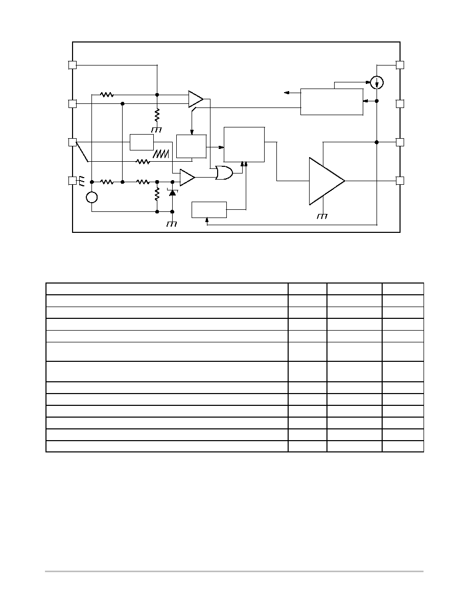
Q
Set
Reset
1 V
HV
1
2
3
4
5
6
7
8
Drv
GND
NC
Current
Sense
Adj
FB
Skip Cycle Comparator
.
.
1.1 V
Overload?
Fault Duration
20 k
19 k
Clock Jittering
57 k
25 k
96 k
25 k
5 V
Figure 2. Internal Circuit Architecture
-
+
-
+
Pull-up Resistor
UVLO High and Low
Internal Regulator
HV Current Source
Q Flip-Flop
D
Cmax
= 75%
Reset
65 kHz
100 kHz
133kHz
Ramp
Compensation
-
+
V
ref
220 ns
L.E.B
$
500 mA
V
CC
Internal V
CC
MAXIMUM RATINGS
Rating
Symbol
Value
Unit
Power Supply Voltage, V
CC
Pin
V
CC
16
V
Maximum Voltage on Low Power Pins (except Pin 8 and Pin 6)
-0.3 to 10
V
Maximum Voltage on Pin 8 (HV), Pin 6 (V
CC
) Decoupled to Ground with 10
m
F
500
V
Maximum Voltage on Pin 8 (HV), Pin 6 (V
CC
) Grounded
450
V
Maximum Current into all Pins except V
CC
(Pin 6) and HV (Pin 8) when 10 V ESD
Diodes are Activated
5.0
mA
Thermal Resistance Junction-to-Air, PDIP7 Version
Thermal Resistance Junction-to-Air, SO-8 Version
R
q
J-A
R
q
J-A
100
178
∞
C/W
Maximum Junction Temperature
T
JMAX
150
∞
C
Temperature Shutdown
TSD
155
∞
C
Hysteresis in Shutdown
30
∞
C
Storage Temperature Range
-60 to +150
∞
C
ESD Capability, HBM Model (All Pins except V
CC
and HV)
2.0
kV
ESD Capability, Machine Model
200
V

NCP1216
http://onsemi.com
4
ELECTRICAL CHARACTERISTICS
(For typical values T
J
= 25
∞
C, for min/max values T
J
= 0
∞
C to +125
∞
C, Maximum T
J
= 150
∞
C,
V
CC
= 11 V unless otherwise noted.)
Characteristic
Pin
Symbol
Min
Typ
Max
Unit
DYNAMIC SELF-SUPPLY
V
CC
Increasing Level at which the Current Source Turns Off
6
VCC
OFF
11.2
12.2
13.4
(Note 1)
V
V
CC
Decreasing Level at which the Current Source Turns On
6
VCC
ON
9.2
10.0
11.0
(Note 1)
V
V
CC
Decreasing Level at which the Latch-off Phase Ends
6
VCC
latch
5.6
V
Internal IC Consumption, No Output Load on Pin 5, F
SW
= 65 kHz
6
I
CC1
990
1110
(Note 2)
m
A
Internal IC Consumption, No Output Load on Pin 5, F
SW
= 100 kHz
6
I
CC1
1025
1180
(Note 2)
m
A
Internal IC Consumption, No Output Load on Pin 5, F
SW
= 133 kHz
6
I
CC1
1060
1200
(Note 2)
m
A
Internal IC Consumption, 1.0 nF Output Load on Pin 5, F
SW
= 65 kHz
6
I
CC2
1.7
2.0
(Note 3)
mA
Internal IC Consumption, 1.0 nF Output Load on Pin 5, F
SW
= 100 kHz
6
I
CC2
2.1
2.4
(Note 3)
mA
Internal IC Consumption, 1.0 nF Output Load on Pin 5, F
SW
= 133 kHz
6
I
CC2
2.4
2.9
(Note 3)
mA
Internal IC Consumption, Latch-off Phase, V
CC
= 6.0 V
6
I
CC3
350
m
A
INTERNAL START-UP CURRENT SOURCE (T
J
> 0
∞
C)
High-voltage Current Source, V
CC
= 10 V
8
IC1
4.9
(Note 4)
8.0
11
mA
High-voltage Current Source, V
CC
= 0 V
8
IC2
9.0
mA
DRIVE OUTPUT
Output Voltage Rise-time @ C
L
= 1.0 nF, 10-90% of a 12 V Output Signal
5
T
r
60
ns
Output voltage fall-time @ C
L
= 1.0 nF, 10-90% of a 12 V Output Signal
5
T
f
20
ns
Source Resistance
5
R
OH
15
20
35
W
Sink Resistance
5
R
OL
5.0
10
18
W
CURRENT COMPARATOR (Pin 5 Unloaded)
Input Bias Current @ 1.0 V Input Level on Pin 3
3
I
IB
0.02
m
A
Maximum Internal Current Setpoint
3
I
Limit
0.93
1.08
1.14
V
Default Internal Current Setpoint for Skip Cycle Operation
3
I
Lskip
330
mV
Propagation Delay from Current Detection to Gate OFF State
3
T
DEL
80
130
ns
Leading Edge Blanking Duration
3
T
LEB
220
ns
1.
V
CC
OFF
and
V
CC
ON
min-max always ensure an hysteresis of 2.0 V.
2. Maximum value at T
J
= 0
∞
C.
3. Maximum value @ T
J
= 25
∞
C, please see characterization curves.
4. Minimum value for T
J
= 125
∞
C.
NCP1216
http://onsemi.com
5
ELECTRICAL CHARACTERISTICS
(continued)
(For typical values T
J
= 25
∞
C, for min/max values T
J
= 0
∞
C to +125
∞
C, Maximum
T
J
= 150
∞
C, V
CC
= 11 V unless otherwise noted.)
Characteristic
Pin
Symbol
Min
Typ
Max
Unit
INTERNAL OSCILLATOR (V
CC
= 11 V, Pin 5 Loaded by 1.0 k
W
)
Oscillation Frequency, 65 kHz Version
f
OSC
58.5
65
71.5
kHz
Oscillation Frequency, 100 kHz Version
f
OSC
90
100
110
kHz
Oscillation Frequency, 133 kHz Version
f
OSC
120
133
146
kHz
Built-in Frequency Jittering in Percentage of f
OSC
f
jitter
±
4.0
%
Maximum Duty-cycle NCP1216
D
max
69
75
81
%
FEEDBACK SECTION (V
CC
= 11 V, Pin 5 Loaded by 1.0 k
W
)
Internal Pull-up Resistor
2
R
up
20
k
W
Pin 2 (FB) to Internal Current Setpoint Division Ratio
-
I
ratio
3.3
SKIP CYCLE GENERATION
Default Skip Mode Level
1
V
skip
0.9
1.1
1.26
V
Pin 1 Internal Output Impedance
1
Z
out
25
k
W
INTERNAL RAMP COMPENSATION
Internal Ramp Level @ 25
∞
C (Note 5)
3
V
ramp
2.6
2.9
3.2
V
Internal Ramp Resistance to C
S
Pin
3
R
ramp
19
k
W
5. A 1.0 M
W
resistor is connected to the ground for the measurement.

NCP1216
http://onsemi.com
6
TEMPERATURE (
∞
C)
Figure 3. High Voltage Pin Leakage Current vs.
Temperature
0
10
20
30
40
50
-25
0
25
50
75
100
125
HV PIN LEAKAGE CURRENT @ 500 V
(
m
A)
Figure 4. VCC
OFF
vs. Temperature
11.0
11.5
12.0
12.5
13.0
13.5
14.0
-25
0
25
50
75
100
125
TEMPERATURE (
∞
C)
VCC
OFF
(V)
Figure 5. VCC
ON
vs. Temperature
9.0
9.5
10.0
10.5
11.0
11.5
12.0
-25
0
25
50
75
100
125
VCC
ON
(V)
TEMPERATURE (
∞
C)
500
600
700
800
900
1000
1100
1200
1300
1400
-25
0
25
50
75
100
125
TEMPERATURE (
∞
C)
I
CC1
(
m
A)
Figure 6. I
CC1
(@ V
CC
= 11 V) vs. Temperature
65 kHz
133 kHz
100 kHz
1.00
1.20
1.40
1.60
1.80
2.00
2.20
2.40
2.60
2.80
-25
0
25
50
75
100
125
TEMPERATURE (
∞
C)
I
CC2
(mA)
133 kHz
100 kHz
65 kHz
Figure 7. I
CC2
vs. Temperature
50
70
90
110
130
150
-25
0
25
50
75
100
125
133 kHz
100 kHz
65 kHz
F
OS
C
(kHz)
TEMPERATURE (
∞
C)
Figure 8. Switching Frequency vs.
Temperature
TYPICAL CHARACTERISTICS

NCP1216
http://onsemi.com
7
5.30
5.40
5.50
5.60
5.70
5.80
5.90
-25
0
25
50
75
100
125
TEMPERATURE (
∞
C)
VCC
latch
(V)
Figure 9. VCC
latch
vs. Temperature
Figure 10. I
CC3
vs. Temperature
200
250
300
350
400
-25
0
25
50
75
100
125
TEMPERATURE (
∞
C)
I
CC3
(
m
A)
0
5
10
15
20
25
30
-25
0
25
50
75
100
125
DRIVER RESIST
ANCE (
W
)
TEMPERATURE (
∞
C)
Figure 11. Drive Sink and Source Resistance
vs. Temperature
Source
Sink
0.93
0.98
1.03
1.08
1.13
-25
0
25
50
75
100
125
TEMPERATURE (
∞
C)
CURRENT SENSE LIMIT (V)
Figure 12. Current Sense Limit vs.
Temperature
65 kHz
133 kHz
100 kHz
-25
0
25
50
75
100
125
1.00
1.05
1.10
1.15
1.20
TEMPERATURE (
∞
C)
V
skip
(V)
Figure 13. V
skip
vs. Temperature
72.0
72.5
73.0
73.5
74.0
74.5
75.0
-25
0
25
50
75
100
125
TEMPERATURE (
∞
C)
DUTY CYCLE (%)
100 kHz
133 kHz
65 kHz
Figure 14. Max Duty-Cycle vs. Temperature

NCP1216
http://onsemi.com
8
2.70
2.75
2.80
2.85
2.90
2.95
3.00
3.05
3.10
-25
0
25
50
75
100
125
TEMPERATURE (
∞
C)
V
ram
p
(V)
Figure 15. V
ramp
vs. Temperature
65 kHz
133 kHz
100 kHz
2
4
6
8
10
12
14
-25
0
25
50
75
100
125
IC1 (mA)
TEMPERATURE (
∞
C)
Figure 16. High Voltage Current Source
(@ V
CC
= 10 V) vs. Temperature

NCP1216
http://onsemi.com
9
APPLICATION INFORMATION
Introduction
The NCP1216 implements a standard current mode
architecture where the switch-off event is dictated by the
peak current setpoint. This component represents the ideal
candidate where low part-count is the key parameter,
particularly in low-cost AC/DC adapters, TV power
supplies etc. Due to its high-performance High-Voltage
technology, the NCP1216 incorporates all the necessary
components normally needed in UC384X based supplies:
timing components, feedback devices, low-pass filter and
self-supply. This later point emphasizes the fact that ON
Semiconductor's NCP1216 does NOT need an auxiliary
winding to operate: the product is naturally supplied from
the high-voltage rail and delivers a V
CC
to the IC. This
system is called the Dynamic Self-Supply (DSS):
Dynamic Self-Supply (DSS): Due to its Very High
Voltage Integrated Circuit (VHVIC) technology,
ON Semiconductor's NCP1216 allows for a direct pin
connection to the high-voltage DC rail. A dynamic current
source charges up a capacitor and thus provides a fully
independent V
CC
level to the NCP1216. As a result, there is
no need for an auxiliary winding whose management is
always a problem in variable output voltage designs (e.g.
battery chargers).
Adjustable Skip Cycle Level: By offering the ability to tailor
the level at which the skip cycle takes place, the designer can
make sure that the skip operation only occurs at low peak
current. This point guarantees a noise-free operation with
cheap transformers. Skip cycle offers a proven mean to
reduce the standby power in no or light loads situations.
Internal Frequency Dithering for Improved EMI
Signature: By modulating the internal switching frequency
with the DSS V
CC
ripple, natural energy spread appears and
softens the controller's EMI signature.
Wide Switching - Frequency Offered with Different
Options (65 kHz - 100 kHz - 133 kHz): Depending on the
application, the designer can pick up the right device to help
reducing magnetics or improve the EMI signature before
reaching the 150 kHz starting point.
Ramp Compensation: By inserting a resistor between the
current-sense (CS) pin and the actual sense resistor, it
becomes possible to inject a given amount of ramp
compensation since the internal sawtooth clock is routed to
the CS pin. Sub-harmonic oscillations in Continuous
Conduction Mode (CCM) can thus be compensated via a
single resistor.
Over Current Protection (OCP): By continuously
monitoring
the FB line activity, NCP1216 enters burst mode
as soon as the power supply undergoes an overload. The
device enters a safe low power operation, which prevents
from any lethal thermal runaway. As soon as the default
disappears, the power supply resumes operation. Unlike
other controllers, overload detection is performed
independently of any auxiliary winding level. In presence of
a bad coupling between both power and auxiliary windings,
the short circuit detection can be severely affected. The DSS
naturally shields you against these troubles.
Wide Duty-
Cycle Operation: Wide mains operation requires
a large duty-cycle excursion. The NCP1216 can go up to 75%
typically. For Continuous Conduction Mode (CCM)
applications, the internal ramp compensation lets you fight
against sub-harmonic oscillations.
Low Stand-By-Power: If SMPS naturally exhibit a good
efficiency at nominal load, they begin to be less efficient
when the output power demand diminishes. By skipping
unnecessary switching cycles, the NCP1216 drastically
reduces the power wasted during light load conditions. In
no-load conditions, the NPC1216 allows the total standby
power to easily reach next International Energy Agency
(IEA) recommendations.
No Acoustic Noise While Operating: Instead of skipping
cycles at high peak currents, the NCP1216 waits until the
peak current demand falls below a user-adjustable 1/3
rd
of
the maximum limit. As a result, cycle skipping can take
place without having a singing transformer, one can thus
select cheap magnetic components free of noise problems.
External MOSFET Connection: By leaving the external
MOSFET external to the IC, you can select avalanche proof
devices, which in certain cases (e.g. low output powers), let
you work without an active clamping network. Also, by
controlling the MOSFET gate signal flow; you have an
option to slow down the device commutation, therefore
reducing the amount of ElectroMagnetic Interference
(EMI).
SPICE Model: A dedicated model to run transient
cycle-by-cycle simulations is available but also an
averaged
version to help you closing the loop. Ready-to-use
templates can be downloaded in OrCAD's PSpice and
INTUSOFT's IsSpice from ON Semiconductor web site, in
the NCP1216 related section.

NCP1216
http://onsemi.com
10
Dynamic Self-Supply
The DSS principle is based on the charge/discharge of the
V
CC
bulk capacitor from a low level up to a higher level. We
can easily describe the current source operation with a bunch
of simple logical equations:
POWER-ON: If V
CC
< VCC
OFF
then the Current Source
is ON, no output pulses
If V
CC
decreasing > VCC
ON
then the Current Source is
OFF, output is pulsing
If V
CC
increasing < VCC
OFF
then the Current Source is
ON, output is pulsing
Typical values are: VCC
OFF
= 12.2 V, VCC
ON
= 10 V
To better understand the operational principle, Figure 17
offers the necessary light:
10
30
50
70
90
Figure 17. The Charge/Discharge Cycle Over a
10
m
F V
CC
Capacitor
VCC
OFF
= 12.2 V
VCC
ON
= 10 V
V
ripple
= 2.2 V
ON, I = 8 mA
OFF, I = 0 mA
Output Pulse
The DSS behavior actually depends on the internal IC
consumption and the MOSFET's gate charge Q
g
. If we
select a 600 V 10 A MOSFET featuring a 30 nC Q
g
, then we
can compute the resulting average consumption supported
by the DSS which is:
Itotal
[
Fsw
Qg
)
ICC1.
(eq. 1)
The total IC heat dissipation incurred by the DSS only is
given by:
Itotal
Vpin8.
(eq. 2)
Suppose that we select the NCP1216P065 with the above
MOSFET, the total current is
(30 n
65 k)
)
900
m +
2.9 mA.
(eq. 3)
Supplied from a 350 VDC rail (250 VAC), the heat
dissipated by the circuit would then be:
350 V
2.9 mA
+
1 W
(eq. 4)
As you can see, it exists a tradeoff where the dissipation
capability of the NCP1216 fixes the maximum Q
g
that the
circuit can drive, keeping its dissipation below a given
target. Please see the "Power Dissipation" section for a
complete design example and discover how a resistor can
help to heal the NCP1216 heat equation.
Application note AND8069/D details tricks to widen the
NCP1216 driving implementation, in particular for large Q
g
MOSFETs. This document can be downloaded at
www.onsemi.com/pub/Collateral/AND8069-D.PDF.
Ramp Compensation
Ramp compensation is a known mean to cure
sub-harmonic oscillations. These oscillations take place at
half the switching frequency and occur only during
Continuous Conduction Mode (CCM) with a duty-cycle
greater than 50%. To lower the current loop gain, one usually
injects between 50% and 100% of the inductor down-slope.
Figure 18 depicts how internally the ramp is generated:
CS
L.E.B
19 k
2.9V
0V
Figure 18. Inserting a Resistor in Series with the
Current Sense Information brings Ramp
Compensation
-
+
From Set-point
R
sense
R
comp
DC
max
= 75
∞
C
In the NCP1216, the ramp features a swing of 2.9 V with
a Duty cycle max at 75%. Over a 65 kHz frequency, it
corresponds to a
2.9
0.75
65 kHz
+
251 mV
m
s ramp.
(eq. 5)
In our FLYBACK design, let's suppose that our primary
inductance L
p
is 350
mH, delivering 12 V with a Np : Ns
ratio of 1:0.1. The OFF time primary current slope is thus
given by:
Vout
)
Vf
Lp
Np
Ns
+
371 mA
m
s or37 mV
m
s
(eq. 6)
when projected over an R
sense
of 0.1
W, for instance. If we
select 75% of the down-slope as the required amount of
ramp compensation, then we shall inject 27 mV/
ms. Our
internal compensation being of 251 mV/
ms, the divider ratio
(divratio) between R
comp
and the 19 k
W is 0.107. A few lines
of algebra to determine R
comp
:
19 k
divratio
1
*
divratio
+
2.37 k
W
(eq. 7)
Frequency Jittering
Frequency jittering is a method used to soften the EMI
signature by spreading the energy in the vicinity of the main
switching component. NCP1216 offers a
$4% deviation of

NCP1216
http://onsemi.com
11
the nominal switching frequency whose sweep is
synchronized
with the V
CC
ripple. For instance, with a 2.2 V
peak-to-peak ripple, the NCP1216P065 frequency will
equal 65 kHz in the middle of the ripple and will increase as
V
CC
rises or decrease as V
CC
ramps down. Figure 19
portrays the behavior we have adopted:
Figure 19. V
CC
Ripple is Used to Introduce a
Frequency Jittering on the Internal Oscillator
Sawtooth
65 kHz
68 kHz
VCC
OFF
V
CC
Ripple
VCC
ON
62 kHz
Skipping Cycle Mode
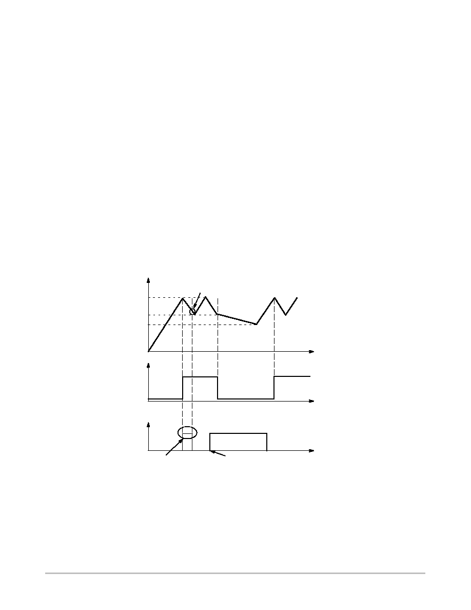
The NCP1216 automatically skips switching cycles when
the output power demand drops below a given level. This is
accomplished by monitoring the FB pin. In normal
operation, pin 2 imposes a peak current accordingly to the
load value. If the load demand decreases, the internal loop
asks for less peak current. When this setpoint reaches a
determined level, the IC prevents the current from
decreasing further down and starts to blank the output
pulses: the IC enters the so-called skip cycle mode, also
named controlled burst operation. The power transfer now
depends upon the width of the pulse bunches (Figure 21).
Suppose we have the following component values:
L
p
, primary inductance = 350
mH
F
sw
, switching frequency = 65 kHz
I
p
skip = 600 mA (or 333 mV / R
sense
)
The theoretical power transfer is therefore:
1
2
Lp
Ip2
Fsw
+
4 W.
(eq. 8)
If this IC enters skip cycle mode with a bunch length of
10 ms over a recurrent period of 100 ms, then the total power
transfer is:
4
0.1
+
400 mW.
(eq. 9)
To better understand how this skip cycle mode takes place,
a look at the operation mode versus the FB level
immediately gives the necessary insight:
Figure 20.
4.2 V, F
B
Pin Open
3.2 V, Upper
Dynamic Range
Normal Current Mode Operation
Skip Cycle Operation
I
pMIN
= 333 mV / R
sense
FB
1 V
When FB is above the skip cycle threshold (1.0 V by
default), the peak current cannot exceed 1.0 V/R
sense
. When
the IC enters the skip cycle mode, the peak current cannot go
below V
pin1
/ 3.3. The user still has the flexibility to alter this
1.0 V by either shunting pin 1 to ground through a resistor
or raising it through a resistor up to the desired level.
Grounding pin 1 permanently invalidates the skip cycle
operation.
Figure 21. Output Pulses at Various Power Levels
(X = 5
m
s/div) P1 < P2 < P3
Power P1
Power
P2
Power
P3
NCP1216
http://onsemi.com
12
315.4U
882.7U
1.450M
2.017M
2.585M
300
200
100
0
Figure 22. The Skip Cycle Takes Place at Low Peak
Currents which Guarantees Noise Free Operation
Skip Cycle
Current Limit
Max Peak
Current
Non-Latching Shutdown
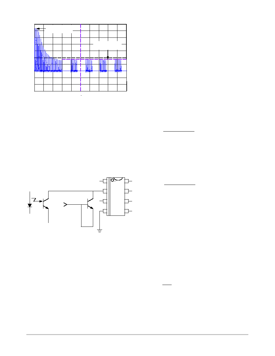
In some cases, it might be desirable to shut off the part
temporarily and authorize its re-start once the default has
disappeared. This option can easily be accomplished
through a single NPN bipolar transistor wired between FB
and ground. By pulling FB below the Adj pin 1 level, the
output pulses are disabled as long as FB is pulled below
pin 1. As soon as FB is relaxed, the IC resumes its operation.
Figure 23 depicts the application example:
1
2
3
4
5
8
6
7
Q1
ON/OFF
Figure 23. Another Way of Shutting Down the IC
without a Definitive Latch-off State
A full latching shutdown, including over-temperature
protection, is described in application note AND8069/D.
Power Dissipation
The NCP1216 is directly supplied from the DC rail
through the internal DSS circuitry. The current flowing
through the DSS is therefore the direct image of the
NCP1216 current consumption. The total power dissipation
can be evaluated using:
(VHVDC
*
11 V)
ICC2
(eq. 10)
which is, as we saw, directly related to the MOSFET Q
g
. If
we operate the device on a 90-250 VAC rail, the maximum
rectified voltage can go up to 350 VDC. However, as the
characterization curves show, the current consumption
drops at a higher junction temperature, which quickly occurs
due to the DSS operation. In our example, at
T
ambient
= 50
∞
C, I
CC2
is measured to be 2.9 mA with a
10 A / 600 V MOSFET. As a result, the NCP1216 will
dissipate from a 250 VAC network,
350 V
2.9 mA@TA
+
50 C
+
1 W
(eq. 11)
∞
The PDIP7 package offers a junction-to-ambient thermal
resistance R
qJ-A
of 100
∞
C/W. Adding some copper area
around the PCB footprint will help decreasing this number:
12 mm x 12 mm to drop R
qJ-A
down to 75
∞
C/W with 35
m
copper thickness (1 oz.) or 6.5 mm x 6.5 mm with 70
m
copper thickness (2 oz.). For a SO-8, the original 178
∞
C/W
will drop to 100
∞
C/W with the same amount of copper. With
this later PDIP7 number, we can compute the maximum
power dissipation that the package accepts at an ambient of
50
∞
C:
P max
+
TJmax
*
TAmax
R
q
J
*
A
+
1 W
(eq. 12)
which barely matches our previous budget. Several
solutions exist to help improving the situation:
1- Insert a Resistor in Series with Pin 8: This resistor will
take a part of the heat normally dissipated by the NCP1216.
Calculations of this resistor imply that V
pin8
does not drop
below 50 V in the lowest mains conditions. Therefore, R
drop
can be selected with:
Rdrop
v
Vbulkmin
*
50 V
8 mA
(eq. 13)
In our case, V
bulk
minimum is 120 VDC, which leads to a
dropping resistor of 8.7 k
W. With the above example in
mind, the DSS will exhibit a duty-cycle of:
2.9 mA 8 mA
+
36%
(eq. 14)
By inserting the 8.7 k
W resistor, we drop
8.7 k
W
* 8 mA
+
69.6 V
(eq. 15)
during the DSS activation. The power dissipated by the
NCP1216 is therefore:
Pinstant * DSSduty
*
cycle
+
(eq. 16)
(350
*
69) * 8 m * 0.36
+
800 mW
We can pass the limit and the resistor will dissipate
(eq. 17)
1 W
*
800 mW
+
200 mW
or
(eq. 18)
pdrop
+
692
8.7 k
* 0.36
2- Select a MOSFET with a Lower Q
g
: Certain MOSFETs
exhibit different total gate charges depending on the
technology they use. Careful selection of this component
can help to significantly decrease the dissipated heat.
NCP1216
http://onsemi.com
13
3- Implement Figure 3, from AN8069/D, Solution: This is
another possible option to keep the DSS functionality (good
short-circuit protection and EMI jittering) while driving any
types of MOSFETs. This solution is recommended when the
designer plans to use SO-8 controllers.
4- Connect an Auxiliary Winding: If the mains conditions
are such that you simply can't match the maximum power
dissipation, then you need to connect an auxiliary winding
to permanently disconnect the start-up source.
Overload Operation
In applications where the output current is purposely not
controlled (e.g. wall adapters delivering raw DC level), it is
interesting to implement a true short-circuit protection. A
short-circuit actually forces the output voltage to be at a low
level, preventing a bias current to circulate in the
Optocoupler LED. As a result, the FB pin level is pulled up
to 4.2 V, as internally imposed by the IC. The peak current
setpoint goes to the maximum and the supply delivers a
rather high power with all the associated effects. Please note
that this can also happen in case of feedback loss, e.g. a
broken Optocoupler. To account for this situation, NCP1216
hosts a dedicated overload detection circuitry. Once
activated, this circuitry imposes to deliver pulses in a burst
manner with a low duty-cycle. The system auto-recovers
when the fault condition disappears.
During the start-up phase, the peak current is pushed to
the maximum until the output voltage reaches its target and
the feedback loop takes over. This period of time depends on
normal output load conditions and the maximum peak
current allowed by the system. The time-out used by this IC
works with the V
CC
decoupling capacitor: as soon as the
V
CC
decreases from the VCC
OFF
level (typically 12.2 V) the
device internally watches for an overload current situation.
If this condition is still present when the VCC
ON
level is
reached, the controller stops the driving pulses, prevents the
self-supply current source to restart and puts all the circuitry
in standby, consuming as little as 350
mA typical (I
CC3
parameter). As a result, the V
CC
level slowly discharges
toward 0 V. When this level crosses 5.6 V typical, the
controller enters a new start-up phase by turning the current
source on: V
CC
rises toward 12.2 V and again delivers
output pulses at the VCC
OFF
crossing point. If the fault
condition has been removed before VCC
ON
approaches,
then the IC continues its normal operation. Otherwise, a new
fault cycle takes place. Figure 24 shows the evolution of the
signals in presence of a fault.
Figure 24.
Latch-off
Phase
Time
Time
Time
Fault is
Relaxed
Regulation
Occurs Here
V
CC
12.2 V
10 V
5.6 V
Fault Occurs Here
Start-up Phase
Internal
Fault Flag
Driver
Pulses
Drv
Driver
Pulses
VCC
OFF
= 12.2 V
VCC
ON
= 10 V
VCC
latch
= 5.6 V
If the fault is relaxed during the V
CC
natural fall down
sequence, the IC automatically resumes.
If the fault still persists when V
CC
reached VCC
ON
, then the
controller cuts everything off until recovery.
Calculating the VCC Capacitor
As the above section describes, the fall down sequence
depends upon the V
CC
level: how long does it take for the
V
CC
line to go from 12.2 V to 10 V
. The required time

NCP1216
http://onsemi.com
14
depends on the start-up sequence of your system, i.e. when
you first apply the power to the IC. The corresponding
transient fault duration due to the output capacitor charging
must be less than the time needed to discharge from 12.2 V
to 10 V, otherwise the supply will not properly start. The test
consists in either simulating or measuring in the lab how
much time the system takes to reach the regulation at full
load. Let's suppose that this time corresponds to 6ms.
Therefore a V
CC
fall time of 10 ms could be well
appropriated in order to not trigger the overload detection
circuitry. If the corresponding IC consumption, including
the MOSFET drive, establishes at 2.9 mA, we can calculate
the required capacitor using the following formula:
D
t
+ D
V∑C
i
(eq. 19)
with
DV = 2.2 V. Then for a wanted Dt of 30 ms, C equals
39.5
mF or a 68 mF for a standard value (including
±
20%
dispersions). When an overload condition occurs, the IC
blocks its internal circuitry and its consumption drops to
350
mA typical. This happens at V
CC
= 10 V and it remains
stuck until V
CC
reaches 5.6 V: we are in latch-off phase.
Again, using the selected 68
mF and 350 mA current
consumption, this latch-off phase lasts: 780 ms.
Protecting the Controller Against Negative Spikes
As with any controller built upon a CMOS technology, it
is the designer's duty to avoid the presence of negative
spikes on sensitive pins. Negative signals have the bad habit
to forward bias the controller substrate and induce erratic
behaviors. Sometimes, the injection can be so strong that
internal parasitic SCRs are triggered, engendering
irremediable damages to the IC if a low impedance path is
offered between V
CC
and GND. If the current sense pin is
often the seat of such spurious signals, the high-voltage pin
can also be the source of problems in certain circumstances.
During the turn-off sequence, e.g. when the user unplugs the
power supply, the controller is still fed by its V
CC
capacitor
and keeps activating the MOSFET ON and OFF with a peak
current limited by R
sense
. Unfortunately, if the quality
coefficient Q of the resonating network formed by L
p
and
C
bulk
is low (e.g. the MOSFET R
dson
+ R
sense
are small),
conditions are met to make the circuit resonate and thus
negatively bias the controller. Since we are talking about ms
pulses, the amount of injected charge,
(Q
=
I
*
t),
immediately latches the controller that brutally discharges
its V
CC
capacitor. If this V
CC
capacitor is of sufficient value,
its stored energy damages the controller. Figure 25 depicts
a typical negative shot occurring on the HV pin where the
brutal V
CC
discharge testifies for latch-up.
Figure 25. A Negative Spike Takes Place on the Bulk Capacitor at the Switch-off Sequence
V
CC
5 V/DIV
10 ms/DIV
V
latch
1 V/DIV
0
Simple and inexpensive cures exist to prevent from
internal parasitic SCR activation. One of them consists in
inserting a resistor in series with the high-voltage pin to
keep the negative current to the lowest when the bulk
becomes negative (Figure 26). Please note that the negative
spike is clamped to (-2 * V
f
) due to the diode bridge. Also,
the power dissipation of this resistor is extremely small since
it only heats up during the start-up sequence.
Another option (Figure 27) consists in wiring a diode
from V
CC
to the bulk capacitor to force V
CC
to reach
VCC
ON
sooner and thus stops the switching activity before
the bulk capacitor gets deeply discharged. For security
reasons, two diodes can be connected in series.

NCP1216
http://onsemi.com
15
Figure 26.
Figure 27.
A simple resistor in series avoids any latch-up in the controller
or one diode forces V
CC
to reach VCC
ON
sooner.
D3
1N4007
1
2
4
5
8
6
7
3
+
+
CV
CC
C
bulk
1
2
4
5
8
6
7
3
+
+
CV
CC
C
bulk
R
bulk
> 4.7 k
ORDERING INFORMATION
Device
Version
Marking
Package
Shipping
NCP1216D065
65 kHz
16D06
SOIC-7
2500 / Tape & Reel
NCP1216D100
100 kHz
16D10
SOIC-7
2500 / Tape & Reel
NCP1216D133
133 kHz
16D13
SOIC-7
2500 / Tape & Reel
NCP1216P065
65 kHz
P1216P065
PDIP-7
50 Units/ Rail
NCP1216P100
100 kHz
P1216P100
PDIP-7
50 Units/ Rail
NCP1216P133
133 kHz
P1216P133
PDIP-7
50 Units/ Rail

NCP1216
http://onsemi.com
16
PACKAGE DIMENSIONS
SO-8
D SUFFIX
CASE 751-07
ISSUE AA
SEATING
PLANE
1
4
5
8
N
J
X 45
_
K
NOTES:
1. DIMENSIONING AND TOLERANCING PER ANSI
Y14.5M, 1982.
2. CONTROLLING DIMENSION: MILLIMETER.
3. DIMENSION A AND B DO NOT INCLUDE MOLD
PROTRUSION.
4. MAXIMUM MOLD PROTRUSION 0.15 (0.006) PER
SIDE.
5. DIMENSION D DOES NOT INCLUDE DAMBAR
PROTRUSION. ALLOWABLE DAMBAR
PROTRUSION SHALL BE 0.127 (0.005) TOTAL IN
EXCESS OF THE D DIMENSION AT MAXIMUM
MATERIAL CONDITION.
6. 751-01 THRU 751-06 ARE OBSOLETE. NEW
STANDARD IS 751-07.
A
B
S
D
H
C
0.10 (0.004)
DIM
A
MIN
MAX
MIN
MAX
INCHES
4.80
5.00
0.189
0.197
MILLIMETERS
B
3.80
4.00
0.150
0.157
C
1.35
1.75
0.053
0.069
D
0.33
0.51
0.013
0.020
G
1.27 BSC
0.050 BSC
H
0.10
0.25
0.004
0.010
J
0.19
0.25
0.007
0.010
K
0.40
1.27
0.016
0.050
M
0
8
0
8
N
0.25
0.50
0.010
0.020
S
5.80
6.20
0.228
0.244
-X-
-Y-
G
M
Y
M
0.25 (0.010)
-Z-
Y
M
0.25 (0.010)
Z
S
X
S
M
_
_
_
_

NCP1216
http://onsemi.com
17
PACKAGE DIMENSIONS
PDIP-7
P SUFFIX
CASE 626B-01
ISSUE A
NOTES:
1. DIMENSIONS AND TOLERANCING PER
ASME Y14.5M, 1994.
2. DIMENSIONS IN MILLIMETERS.
3. DIMENSION L TO CENTER OF LEAD
WHEN FORMED PARALLEL.
4. PACKAGE CONTOUR OPTIONAL
(ROUND OR SQUARE CORNERS).
5. DIMENSIONS A AND B ARE DATUMS.
1
4
5
8
F
NOTE 2
-T-
SEATING
PLANE
H
J
G
D
K
N
C
L
M
M
A
M
0.13 (0.005)
B
M
T
DIM
MIN
MAX
MILLIMETERS
A
9.40
10.16
B
6.10
6.60
C
3.94
4.45
D
0.38
0.51
F
1.02
1.78
G
2.54 BSC
H
0.76
1.27
J
0.20
0.30
K
2.92
3.43
L
7.62 BSC
M
---
10
N
0.76
1.01
∞
A
B

NCP1216
http://onsemi.com
18
ON Semiconductor and are registered trademarks of Semiconductor Components Industries, LLC (SCILLC). SCILLC reserves the right to make
changes without further notice to any products herein. SCILLC makes no warranty, representation or guarantee regarding the suitability of its products for any
particular purpose, nor does SCILLC assume any liability arising out of the application or use of any product or circuit, and specifically disclaims any and all
liability, including without limitation special, consequential or incidental damages. "Typical" parameters which may be provided in SCILLC data sheets and/or
specifications can and do vary in different applications and actual performance may vary over time. All operating parameters, including "Typicals" must be
validated for each customer application by customer's technical experts. SCILLC does not convey any license under its patent rights nor the rights of others.
SCILLC products are not designed, intended, or authorized for use as components in systems intended for surgical implant into the body, or other applications
intended to support or sustain life, or for any other application in which the failure of the SCILLC product could create a situation where personal injury or death
may occur. Should Buyer purchase or use SCILLC products for any such unintended or unauthorized application, Buyer shall indemnify and hold SCILLC
and its officers, employees, subsidiaries, affiliates, and distributors harmless against all claims, costs, damages, and expenses, and reasonable attorney fees
arising out of, directly or indirectly, any claim of personal injury or death associated with such unintended or unauthorized use, even if such claim alleges that
SCILLC was negligent regarding the design or manufacture of the part. SCILLC is an Equal Opportunity/Affirmative Action Employer.
PUBLICATION ORDERING INFORMATION
JAPAN: ON Semiconductor, Japan Customer Focus Center
2-9-1 Kamimeguro, Meguro-ku, Tokyo, Japan 153-0051
Phone: 81-3-5773-3850
ON Semiconductor Website: http://onsemi.com
For additional information, please contact your local
Sales Representative.
NCP1216/D
The product described herein (NCP1216), may be covered by the following U.S. patents: 6,385,060; 6,587,357. There may be other
patents pending.
Literature Fulfillment:
Literature Distribution Center for ON Semiconductor
P.O. Box 5163, Denver, Colorado 80217 USA
Phone: 303-675-2175 or 800-344-3860 Toll Free USA/Canada
Fax: 303-675-2176 or 800-344-3867 Toll Free USA/Canada
Email: orderlit@onsemi.com
N. American Technical Support: 800-282-9855 Toll Free USA/Canada