 | –≠–ª–µ–∫—Ç—Ä–æ–Ω–Ω—ã–π –∫–æ–º–ø–æ–Ω–µ–Ω—Ç: NCP1280 | –°–∫–∞—á–∞—Ç—å:  PDF PDF  ZIP ZIP |
©
Semiconductor Components Industries, LLC, 2004
April, 2004 - Rev. 1
1
Publication Order Number
NCP1280/D
NCP1280
Active Clamp Voltage Mode
PWM Controller for Off-Line
Applications
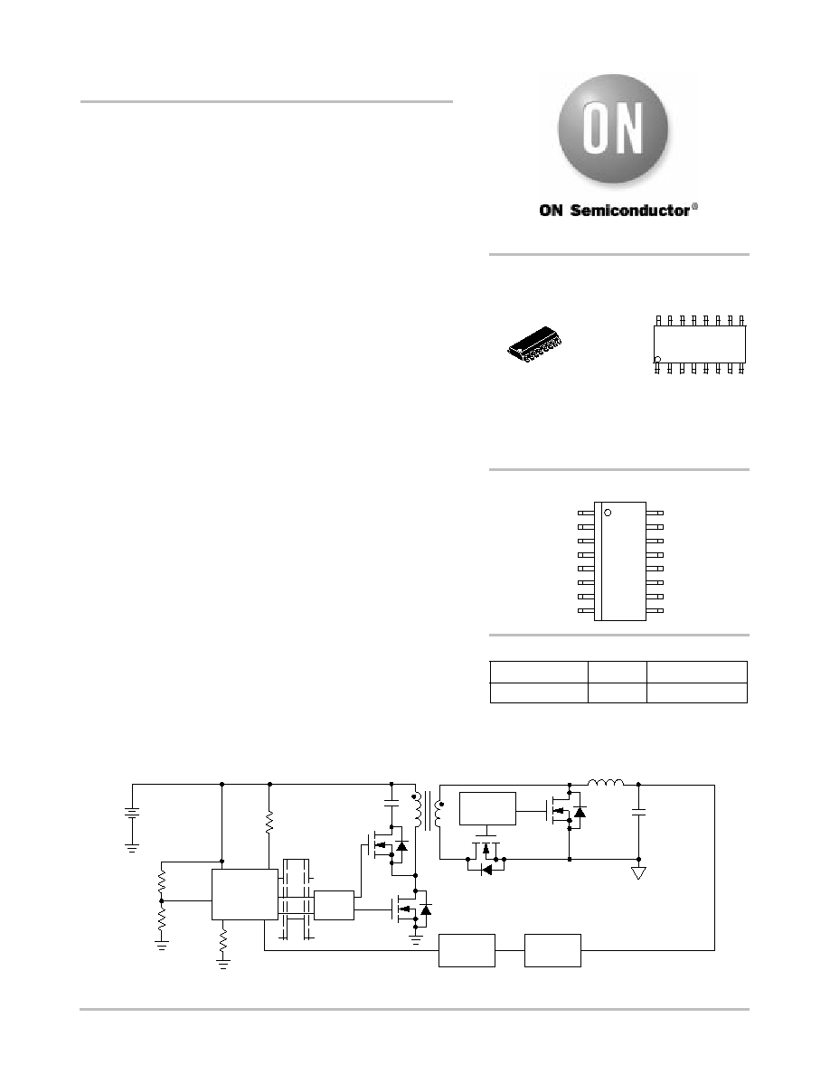
The NCP1280 provides a highly integrated solution for off-line
power supplies requiring high-efficiency and low parts count. This
voltage mode controller provides control outputs for driving a forward
converter primary MOSFET and an auxiliary MOSFET for active
clamp circuit. The second output with its programmable delay can also
be used for driving a synchronous rectifier on the secondary or for
asymmetric half bridge circuits. Incorporation of high voltage start-up
circuitry (with 700 V capability) reduces parts count and system
power dissipation. Additional features such as line UV/OV protection,
soft start, single resistor programmable (high) frequency oscillator,
line voltage feedforward, dual mode overcurrent protection and
maximum duty cycle control, allow converter optimization at minimal
cost. Compared to a traditional forward converter, an NCP1280 based
converter can offer significant efficiency improvements and system
cost savings.
Features
∑
Internal High Voltage Start-Up Regulator (25 V to 700 V)
∑
Dual Control Outputs with Adjustable Overlap Delay
∑
Programmable Maximum Duty Cycle Control
∑
Single Resistor Oscillator Frequency Setting
∑
Fast Line Feedforward
∑
Line Under/Overvoltage Lockout
∑
Dual Mode Overcurrent Protection
∑
Programmable Soft Start
∑
Precision 5.0 V Reference
Typical Applications
∑
Off-Line Power Converters in 100-500 W Range
∑
Desktop Power Supplies (High-End)
∑
Industrial Power Supplies
∑
Plasma/LCD TV Front-End
TX1
NCP1280
+
-
Driver
Opto
Error
Amplifier
Start-up
Feedforward
(100 V - 425 V)
UV/OV
Overlap
Delay
+
-
V
in
V
out
(3.3 V)
C
out
L
out
Figure 1. Forward Converter for Off-line Applications Using PFC Inputs
C
clamp
OUT1
OUT2
V
in
FF
t
D
Drive
SR
Device
Package
Shipping
ORDERING INFORMATION
NCP1280DR2
SO-16
2500/Tape & Reel
NCP1280 = Device Code
A
= Assembly Location
WL
= Wafer Lot
Y
= Year
WW
= Work Week
MARKING
DIAGRAM
16
SO-16
D SUFFIX
CASE 751B
NCP1280
1
1
16
AWLYWW
http://onsemi.com
PIN CONNECTIONS
SS
DC
MAX
1
16
V
EA
R
T
V
REF
C
SKIP
t
D
CS
OUT2
FF
GND
UV/OV
OUT1
NC
V
AUX
V
in
For information on tape and reel specifications,
including part orientation and tape sizes, please
refer to our Tape and Reel Packaging Specifications
Brochure, BRD8011/D.

NCP1280
http://onsemi.com
2
Figure 2. NCP1280 Functional Block Diagram
+
-
+
5.0 V Reference
V
in
GND
V
EA
Delay
Logic
OUT1
-
+
-
+
-
+
CS
S
R
Q
C
SS
10
5
14
16
1
11
12
R
D
STOP
STOP
V
in
Disable
C
CSKIP
Clock
Disable_ss
S
R
Q
Monotonic
Start
(250 ns)
Disable_ss
C
AUX
DIS
V
AUX
V
AUX
OUT2
V
AUX
15
13
V
AUX
10 pF
FF Ramp
(Adjustable)
* Trimmed during
manufacturing to obtain
1.3 V with R
T
= 101 k
W
V
in
R
FF
FF
4
+
CURRENT MIRROR
-
+
R
T
2 V
10 pF
I
1
+
-
-
2 V
7
Oscillator Ramp
2 V
+
-
DIS
DIS
8
+ -
2 V
Max DC
Comparator
PWM
Comparator
+
-
Soft Start
Comparator
0.5 V
+
-
0.6 V
+
-
SS
9
One Shot
Pulse
-
+
6
CSKIP
3.6 V
1.49 V
3
UV/OV
-
+
2 V
+
-
One Shot
Pulse
+
-
+
-
I
1
2
+
-
1.3 V*
V
REF
t
D
-
20 k
W
40 k
W
V
REF
DC
MAX
2 k
W
32 k
W
27 k
W
5.3 k
W
6.7 k
W
+
V
DC(inv)
-
R
MDP
R
P
C
FF
Disable_V
REF
Disable_V
REF
I
FF
Disable
11
m
A
+
V
-
-
+
I
+
V
125 k
W
R
T
(600 ns)
One Shot
Pulse
Clock
V
REF
V
REF
Output
Latch
(Reset
Dominant)
Latch
(Reset
Dominant)
I
START
V
AUX(ON)
/V
AUX(OFF)
6
m
A

NCP1280
http://onsemi.com
3
PIN DESCRIPTION
Pin
Name
Application Information
1
V
in
This pin is connected to the input voltage of the system. The voltage can be a rectified, filtered line voltage
or output of a power factor correction (PFC) front end. A constant current source supplies current from this
pin to the capacitor connected on the V
AUX
pin. The charge current is typically 13.8 mA. Maximum input
voltage is 700 V.
2
NC
Not Connected.
3
UV/OV
Provides protection under line undervoltage and overvoltage conditions. The built in voltage range is
X
2:1. If needed, the OV function can be disabled by a zener from this pin to ground.
4
FF
An external resistor between V
in
and this pin adjusts the amplitude of the Feedforward Ramp in proportion
to V
in
. By varying the feedforward ramp amplitude in proportion to the input voltage, open loop line
regulation is improved.
5
CS
Overcurrent sense input. If the CS voltage exceeds 0.48 V or 0.57 V, the converter enters the Cycle by
Cycle or Cycle Skip current limit mode, respectively.
6
CSKIP
The capacitor connected between this pin and ground sets the Cycle Skip period. A soft start sequence
follows at the conclusion of the fault period.
7
R
T
A single external resistor between this pin and GND sets the oscillator fixed frequency.
8
DC
MAX
An external resistor between this pin and GND sets the voltage on the Max DC Comparator inverting
input. The duty cycle is limited by comparing the voltage on the Max DC Comparator inverting input to the
Feedforward Ramp.
9
SS
An internal 6.2
m
A current source charges the external capacitor connected to this pin. The duty cycle is
limited during start-up by comparing the voltage on this pin to the Oscillator Ramp.
10
V
EA
The error signal from an external error amplifier, typically supplied through an optocoupler, is fed into this
input and compared to the Feedforward Ramp. A series diode and resistor offset the voltage on this pin
before it is applied to the PWM Comparator inverting input.
11
V
REF
Precision 5.0 V reference output. Maximum output current is 6 mA.
12
t
D
An external resistor between V
REF
and this pin sets the overlap delay between OUT1 and OUT2
transitions.
13
OUT2
Output of the PWM controller with leading and trailing edge overlap delay. OUT2 can be used to drive a
synchronous rectifier topology, an active clamp/reset switch, or both.
14
GND
Control circuit ground.
15
OUT1
Main output of the PWM controller.
16
V
AUX
Positive input supply voltage. This pin is connected to an external capacitor for energy storage. An
internal current supplies current from V
in
to this pin. Once the voltage on V
AUX
reaches 11 V, the current
source turns OFF. It turns ON again once V
AUX
falls to 7 V. During normal operation, power is supplied to
the IC via this pin, by means of an auxiliary winding.

NCP1280
http://onsemi.com
4
MAXIMUM RATINGS
(Note 1)
Rating
Symbol
Value
Unit
Input Line Voltage
V
in
-0.3 to 700
V
Auxiliary Supply Voltage
V
AUX
-0.3 to 16
V
Auxiliary Supply Input Current
I
AUX
35
mA
OUT1 and OUT2 Voltage
V
OUT
-0.3 to (V
AUX
+ 0.3 V)
V
OUT1 and OUT2 Output Current
I
OUT
10
mA
5.0 V Reference Voltage
V
REF
-0.3 to 6.0
V
5.0 V Reference Output Current
I
REF
6.0
mA
All Other Inputs/Outputs Voltage
V
IO
-0.3 to V
REF
V
All Other Inputs/Outputs Current
I
IO
10
mA
Operating Junction Temperature
T
J
-40 to 125
∞
C
Storage Temperature Range
T
stg
-55 to 150
∞
C
Power Dissipation at T
A
= 25
∞
C
P
D
0.77
W
Thermal Resistance, Junction to Ambient
R
q
JA
130
∞
C/W
1. Maximum Ratings are those values beyond which damage to the device may occur. Exposure to these conditions or conditions beyond those
indicated may adversely affect device reliability. Functional operation under absolute maximum-rated conditions is not implied. Functional
operation should be restricted to the Recommended Operating Conditions.
A. This device series contains ESD protection and exceeds the following tests:
Pin 1 is the HV start-up of the device and is rated to the max rating of the part, or 700 V.
Machine Model Method 700 V.
Pins 2-16: Human Body Model 4000 V per MIL-STD-883, Method 3015.
Machine Model Method 200 V.
NCP1280
http://onsemi.com
5
ELECTRICAL CHARACTERISTICS
(V
in
= 82 V, V
AUX
= 12 V, V
EA
= 2 V, R
T
= 101 k
W
,
C
CSKIP
= 6800 pF,
R
D
= 60.4 k
W
, R
FF
= 1.0 M
W
, for typical values T
J
= 25
∞
C, for min/max values, T
J
= -40
∞
C to 125
∞
C, unless otherwise noted)
Characteristic
Symbol
Min
Typ
Max
Unit
START-UP CONTROL AND V
AUX
REGULATOR
V
AUX
Regulation
Start-up Threshold/V
AUX
Regulation Peak (V
AUX
increasing)
Minimum Operating V
AUX
Valley Voltage After Turn-On
Hysteresis
V
AUX(on)
V
AUX(off)
V
H
10.5
6.6
-
11.0
7.0
4.0
11.5
7.4
-
V
Minimum Start-up Voltage (Pin 1)
I
START
= 1.5 mA, V
AUX
= V
AUX(on)
- 0.2 V, I
REF
= 0 A
V
START(min)
-
-
25
V
Start-up Circuit Output Current
V
AUX
= 0 V
T
J
= 25
∞
C
T
J
= -40
∞
C to 125
∞
C
V
AUX
= V
AUX(on)
- 0.2 V
T
J
= 25
∞
C
T
J
= -40
∞
C to 125
∞
C
I
START
13
10
10
8
17.5
-
13.8
-
21
25
17
19
mA
Start-up Circuit Off-State Leakage Current (V
in
= 700 V)
T
J
= 25
∞
C
T
J
= -40
∞
C to 125
∞
C
I
START(off)
-
-
23
-
50
100
m
A
Start-up Circuit Breakdown Voltage (Note 2)
I
START(off)
= 50
m
A, T
J
= 25
∞
C
V
(BR)DS
700
-
-
V
Auxiliary Supply Current After V
AUX
Turn-On
Outputs Disabled
V
EA
= 0 V
V
UV/OV
= 0.7 V
Outputs Enabled
I
AUX1
I
AUX2
I
AUX3
-
-
-
2.7
1.3
4.6
5.0
2.5
6.5
mA
LINE UNDER/OVERVOLTAGE DETECTOR
Undervoltage Threshold (V
in
Increasing)
V
UV
1.40
1.52
1.64
V
Undervoltage Hysteresis
V
UV(H)
0.080
0.098
0.120
V
Overvoltage Threshold (V
in
Increasing)
V
OV
3.47
3.61
3.75
V
Overvoltage Hysteresis
V
OV(H)
-
0.145
-
V
Undervoltage Propagation Delay to Output
t
UV
-
250
-
ns
Overvoltage Propagation Delay to Output
t
OV
-
160
-
ns
CURRENT LIMIT
Cycle by Cycle Threshold Voltage
I
LIM1
0.44
0.48
0.52
V
Propagation Delay to Output (V
EA
= 2.0 V)
V
CS
= I
LIM1
to 2.0 V, measured when V
OUT
reaches 0.5 V
OH
t
ILIM
-
90
150
ns
Cycle Skip Threshold Voltage
I
LIM2
0.54
0.57
0.62
V
Cycle Skip Charge Current (V
CSKIP
= 0 V)
I
CSKIP
8.0
12.3
15
m
A
2. Guaranteed by design only.

NCP1280
http://onsemi.com
6
ELECTRICAL CHARACTERISTICS
(V
in
= 82 V, V
AUX
= 12 V, V
EA
= 2 V, R
T
= 101 k
W
, C
CSKIP
= 6800 pF,
R
D
= 60.4 k
W
, R
FF
= 1.0 M
W
, for typical values T
J
= 25
∞
C, for min/max values, T
J
= -40
∞
C to 125
∞
C, unless otherwise noted)
Characteristic
Symbol
Min
Typ
Max
Unit
OSCILLATOR
Frequency (R
T
= 101 k
W
)
T
J
= 25
∞
C
T
J
= -40
∞
C to 125
∞
C
f
OSC1
285
280
300
-
315
320
kHz
Frequency (R
T
= 220 k
W
, V
EA
= 1.0 V)
T
J
= 25
∞
C
T
J
= -40
∞
C to 125
∞
C
f
OSC2
142
140
150
-
158
160
kHz
MAXIMUM DUTY CYCLE COMPARATOR
Maximum Duty Cycle (V
EA
= 3.0 V, T
J
= 25
∞
C)
R
P
= 0
W
, R
MDP
= open
R
P
= open, R
MDP
= open
DC
MAX
57
75
62
80
66
85
%
Open Circuit Voltage
V
DCMAX
0.40
0.47
0.60
V
SOFT START
Charge Current (V
SS
= 1.0 V)
I
SS(C)
5.0
6.2
7.4
m
A
Discharge Current (V
SS
= 5.0 V, V
UV/OV
= 0 V)
I
SS(D)
20
52.5
-
mA
PWM COMPARATOR
Input Resistance (V
1
= 1.25 V, V
2
= 1.50 V)
R
IN(VEA)
= (V
2
- V
1
)/(I
2
- I
1
)
R
IN(VEA)
8.0
22
60
k
W
Lower Input Threshold
V
EA(L)
0.3
0.7
0.9
V
Delay to Output (from V
OH
to 0.5 V
OH
)
t
PWM
-
200
-
ns
5.0 V REFERENCE
Output Voltage (I
REF
= 0 mA)
T
J
= 25
∞
C
T
J
= -40
∞
C to 125
∞
C
V
REF
4.9
4.8
5.0
-
5.1
5.1
V
Load Regulation (I
REF
= 0 to 6 mA)
V
REF(Load)
-
10
50
mV
Line Regulation (V
AUX
= 7.5 to 16 V)
V
REF(Line)
-
50
100
mV
CONTROL OUTPUTS
Output Voltage (I
OUT
= 0 mA)
Low State
High State
V
OL
V
OH
-
-
0.25
11.8
-
-
V
Overlap Delay
R
D
= 1 M
W
Leading
Trailing
R
D
= 60 k
W
Leading
Trailing
t
D
-
-
50
32
200
170
90
72
-
-
130
130
ns
Drive Resistance (V
in
= 15 V)
Sink (V
EA
= 0 V, V
OUT
= 2 V)
Source (V
EA
= 3 V, V
OUT
= 10 V)
R
SNK
R
SRC
20
50
40
90
80
170
W
Rise Time (C
L
= 100 pF, 10% to 90% of V
OH
)
t
on
-
30
-
ns
Fall Time (C
L
= 100 pF, 90% to 10% of V
OH
)
t
off
-
12
-
ns

NCP1280
http://onsemi.com
7
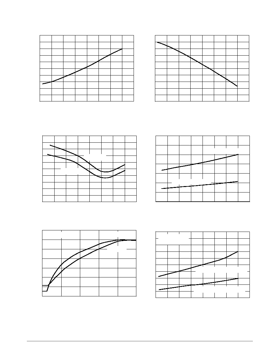
TYPICAL CHARACTERISTICS
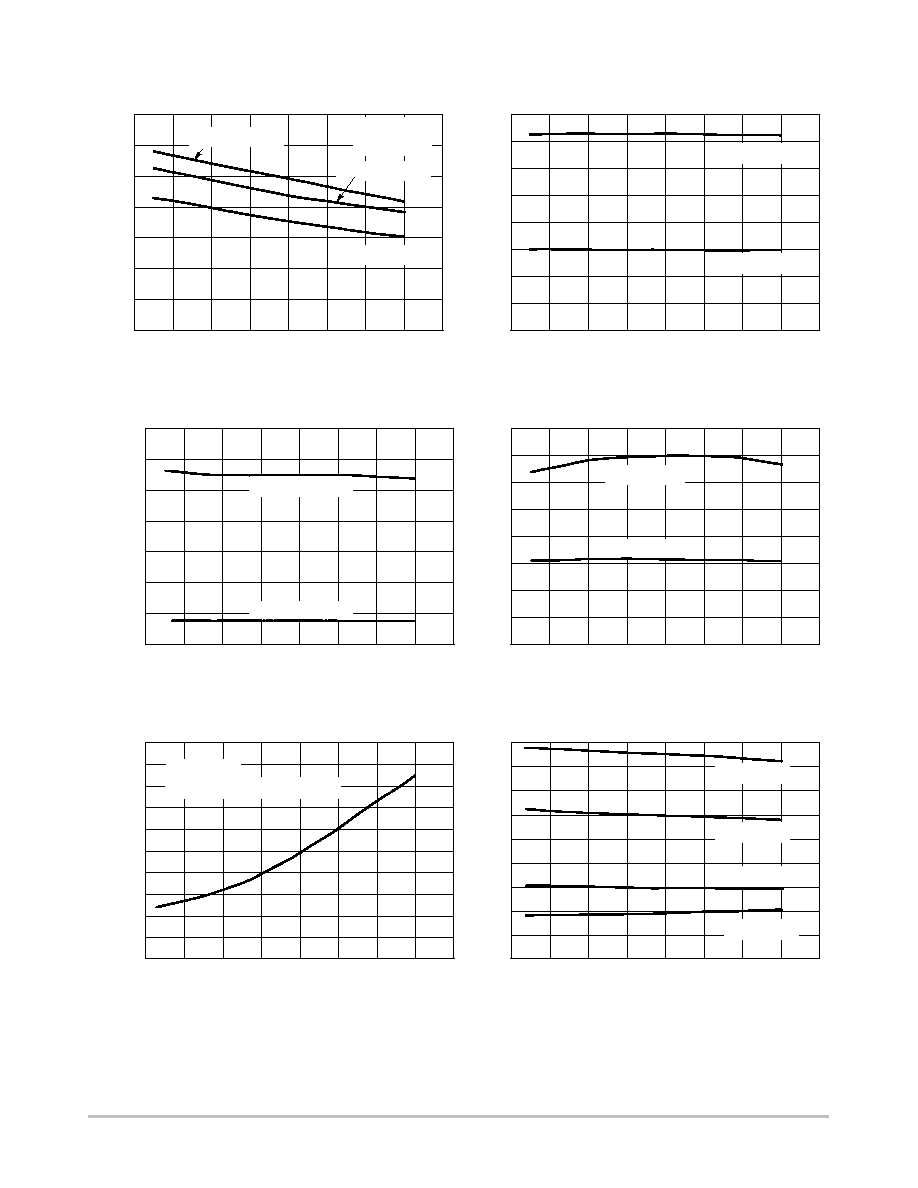
Figure 3. Auxiliary Supply Voltage Thresholds
versus Junction Temperature
Figure 4. Start-up Circuit Output Current
versus Junction Temperature
T
J
, JUNCTION TEMPERATURE (
∞
C)
T
J
, JUNCTION TEMPERATURE (
∞
C)
125
100
75
50
25
0
-25
-50
5
6
7
8
9
10
11
12
125
100
75
50
25
0
-25
-50
10
11
12
13
14
15
16
Figure 5. Start-up Circuit Output Current
versus Auxiliary Supply Voltage
Figure 6. Start-up Circuit Output Current
versus Line Voltage
V
AUX
, AUXILIARY SUPPLY VOLTAGE (V)
V
in
, LINE VOLTAGE (V)
12
10
8
6
4
2
0
13.5
14.0
14.5
15.0
15.5
16.0
16.5
700
600
400
300
200
100
0
0
4
8
12
16
20
Figure 7. Start-up Circuit Off-State Leakage
Current versus Line Voltage
Figure 8. Auxiliary Supply Current versus
Junction Temperature
V
in
, LINE VOLTAGE (V)
T
J
, JUNCTION TEMPERATURE (
∞
C)
600
500
400
300
200
100
0
0
5
10
15
20
25
30
40
125
100
75
50
25
0
-25
-50
0
0.5
1.0
1.5
2.0
2.5
3.5
4.0
V
AUX
, AUXILIAR
Y SUPPL
Y VOL
T
AGE (V)
150
150
17
18
19
I
ST
AR
T
, ST
AR
T-UP CIRCUIT OUTPUT
CURRENT (mA)
17.0
I
ST
AR
T
, ST
AR
T-UP CIRCUIT OUTPUT
CURRENT (mA)
I
ST
AR
T
, ST
AR
T-UP CIRCUIT OUTPUT
CURRENT (mA)
35
I
ST
AR
T(
of
f)
, ST
AR
T-UP CIRCUIT OFF-
ST
A
TE LEAKAGE CURRENT (
m
A)
150
3.0
I
AUX
, AUXILIAR
Y SUPPL
Y CURRENT (mA)
START-UP
THRESHOLD
MINIMUM
OPERATING
THRESHOLD
V
AUX
= 0 V
V
AUX
= V
AUX(on)
- 0.2 V
T
J
= -40
∞
C
T
J
= 25
∞
C
T
J
= -40
∞
C
T
J
= 25
∞
C
T
J
= 125
∞
C
V
EA
= 0 V
V
UV/OV
= 0 V
V
AUX
= 12 V
V
in
= 82 V
V
in
= 82 V
V
AUX
= V
AUX(on)
- 0.2 V
V
AUX
= 12 V
500
9
13.0
T
J
= 125
∞
C
50
45
700
800
900
NCP1280
http://onsemi.com
8
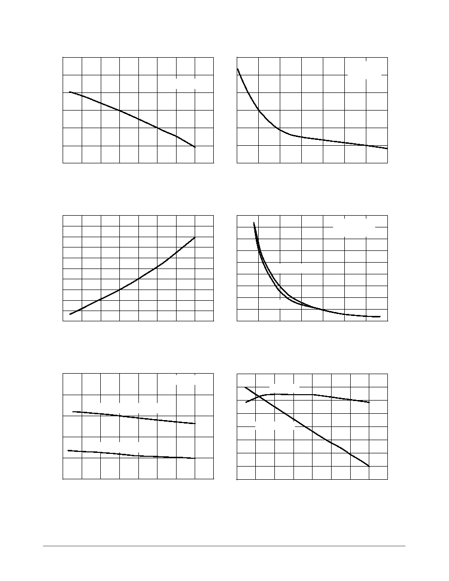
TYPICAL CHARACTERISTICS
Figure 9. Operating Auxiliary Supply Current
versus Junction Temperature
Figure 10. Line Under/Overvoltage Thresholds
versus Junction Temperature
T
J
, JUNCTION TEMPERATURE (
∞
C)
T
J
, JUNCTION TEMPERATURE (
∞
C)
125
100
75
50
25
0
-25
-50
0
1
2
3
4
5
6
7
125
100
75
50
25
0
-25
-50
0
0.5
1.0
1.5
2.0
4.0
Figure 11. Line Under/Overvoltage Thresholds
Hysteresis versus Junction Temperature
T
J
, JUNCTION TEMPERATURE (
∞
C)
150
125
100
25
0
-25
-50
90
100
110
120
130
140
160
Figure 12. Current Limit Thresholds versus
Junction Temperature
T
J
, JUNCTION TEMPERATURE (
∞
C)
125
100
75
50
25
0
-25
-50
400
425
450
475
500
525
575
600
I
AUX3
, OPERA
TING AUXILIAR
Y
SUPPL
Y CURRENT (mA)
150
150
2.5
3.0
3.5
V
UV/OV
, UV/OV VOL
T
AGE (V)
150
V
UV/OV(H)
, UV/OV THRESHOLD
VOL
T
AGE HYSTERESIS (mV)
150
550
I
LIM
, CURRENT LIMIT THRESHOLDS (mV)
75
50
f
OSC
= 440 kHz
UV THRESHOLD
OV THRESHOLD
UV HYSTERESIS
CYCLE SKIP
CYCLE BY CYCLE
V
AUX
= 12 V
DC
[
50%
f
OSC
= 300 kHz
f
OSC
= 87 kHz
OV HYSTERESIS
Figure 13. Current Limit Propagation Delay
versus Junction Temperature
T
J
, JUNCTION TEMPERATURE (
∞
C)
125
100
75
50
25
0
-25
-50
70
75
80
85
90
95
115
120
t
ILIM
, CURRENT LIMIT
PROP
AGA
TION DELA
Y (ns)
150
100
105
110
V
AUX
= 12 V
Measured from V
OH
to 0.5 V
OH
Figure 14. Oscillator Frequency versus
Junction Temperature
T
J
, JUNCTION TEMPERATURE (
∞
C)
125
100
75
50
25
0
-25
-50
0
50
100
150
200
250
450
150
300
350
400
f
osc
, OSCILLA
T
OR FREQUENCY (kHz)
R
T
= 390 k
W
R
T
= 101 k
W
R
T
= 68 k
W
R
T
= 220 k
W
NCP1280
http://onsemi.com
9
TYPICAL CHARACTERISTICS
T
J
, JUNCTION TEMPERATURE (
∞
C)
125
100
75
50
25
0
-25
-50
3.0
3.5
4.0
4.5
5.0
5.5
6.5
7.0
150
6.0
I
SS(
C)
, SOFT ST
AR
T CHARGE CURRENT (
m
A)
30
35
40
45
50
55
65
70
60
CHARGE
DISCHARGE
Figure 15. Oscillator Frequency versus
Junction Temperature
Figure 16. Oscillator Frequency versus
Timing Resistor
R
T
, TIMING RESISTOR (k
W
)
400
300
250
200
150
100
50
0
100
200
300
400
600
500
f
osc
, OSCILLA
T
OR FREQUENCY (kHz)
350
T
J
, JUNCTION TEMPERATURE (
∞
C)
125
100
75
50
25
0
-25
-50
285
290
295
300
305
310
150
315
f
osc
, OSCILLA
T
OR FREQUENCY (kHz)
R
T
= 101 k
W
T
J
= 25
∞
C
DC
[
50%
525
450
225
150
75
0
0
10
20
40
60
90
DC
MAX
, MAXIMUM DUTY CYCLE (%)
375
300
30
50
T
J
= -40
∞
C
T
J
= 125
∞
C
80
70
V
EA
= 3.0 V
V
DCMAX
= 0 V
T
J
, JUNCTION TEMPERATURE (
∞
C)
150
125
100
75
0
-25
-50
50
60
70
80
90
100
DC
MAX
, MAXIMUM DUTY CYCLE (%)
50
25
R
P
= OPEN, R
MDP
= OPEN
R
P
= 0
W
, R
MDP
= OPEN
R
FF
= 1.0 M
W
Figure 17. Feedforward Internal Resistance
versus Junction Temperature
150
125
100
75
0
-25
-50
9
10
11
12
13
14
15
19
17
FEEDFOR
W
ARD INTERNAL RESIST
ANCE (k
W
)
50
25
16
18
Figure 18. Maximum Duty Cycle versus
Feedforward Current
Figure 19. Maximum Duty Cycle versus
Junction Temperature
Figure 20. Soft Start Charge/Discharge
Currents versus Junction Temperature
I
SS(
D)
, SOFT ST
AR
T DISCHARGE CURRENT (mA)
T
J
, JUNCTION TEMPERATURE (
∞
C)
I
FF
, FEEDFORWARD CURRENT (
m
A)
NCP1280
http://onsemi.com
10
TYPICAL CHARACTERISTICS
T
J
, JUNCTION TEMPERATURE (
∞
C)
125
100
75
50
25
0
-25
-50
4.93
4.95
4.97
4.99
5.03
T
J
, JUNCTION TEMPERATURE (
∞
C)
R
D
, DELAY RESISTOR (k
W
)
75
50
25
0
-25
-50
0
50
100
150
200
250
350
1000
800
600
400
200
0
50
75
100
125
150
225
T
J
, JUNCTION TEMPERATURE (
∞
C)
150
125
100
25
0
-25
-50
0
40
80
160
200
150
V
REF
, REFERENCE VOL
T
AGE (V)
300
t
D
, OUTPUTS OVERLAP DELA
Y (ns)
t
D
, OUTPUTS OVERLAP DELA
Y (ns)
R
SNK/SRC
OUTPUTS DRIVE RESIST
ANCE (
W
)
150
125
100
175
200
50
75
120
R
D
= 1 M
W
, LEADING
R
D
= 60 k
W
, LEADING
LEADING
TRAILING
R
SRC
(V
EA
= 0 V, V
OUT
= 10 V)
R
SNK
(V
EA
= 3 V, V
OUT
= 2 V)
V
AUX
= 12 V
R
MDP
= 100 k
W
T
J
= 25
∞
C
I
REF
= 0 mA
I
REF
= 6 mA
5.01
T
J
, JUNCTION TEMPERATURE (
∞
C)
150
125
100
25
0
-25
-50
0.35
0.45
0.55
0.75
0.85
V
EA(
L)
, PWM COMP
ARA
T
OR LOWER
INPUT THRESHOLD (V)
50
75
0.65
Figure 21. V
EA
Input Resistance versus
Junction Temperature
T
J
, JUNCTION TEMPERATURE (
∞
C)
150
100
50
0
-50
0
10
20
40
50
30
R
IN(
VEA)
, V
EA
INPUT RESIST
ANCE (k
W
)
-25
125
75
25
Figure 22. PWM Comparator Lower Input
Threshold versus Junction Temperature
Figure 23. Reference Voltage versus Junction
Temperature
Figure 24. Outputs Overlap Delay versus
Junction Temperature
Figure 25. Outputs Overlap Delay versus
Delay Resistor
Figure 26. Outputs Drive Resistance Voltage
versus Junction Temperature

NCP1280
http://onsemi.com
11
TYPICAL CHARACTERISTICS
Figure 27. Outputs Rise Time versus Load
Capacitance
C
L
, LOAD CAPACITANCE (pF)
200
150
100
50
0
0
10
20
30
40
50
60
80
Figure 28. Outputs Fall Time versus Load
Capacitance
C
L
, LOAD CAPACITANCE (pF)
200
150
100
50
0
0
5
10
15
20
25
35
70
t
on
, OUTPUTS RISE TIME (ns)
30
t
of
f
, OUTPUTS F
ALL TIME (ns)
T
J
= -40
∞
C
T
J
= 25
∞
C
T
J
= 125
∞
C
T
J
= -40
∞
C
T
J
= 25
∞
C
T
J
= 125
∞
C
175
125
75
25
175
125
75
25
Measured from 10% to 90% of V
OH
V
AUX
= 12 V
Measured from 90% to 10% of V
OH
V
AUX
= 12 V
DETAILED OPERATING DESCRIPTION
Introduction
An NCP1280 based system offers significant efficiency
improvements and system cost savings over a converter
using a traditional forward topology. The NCP1280
provides two control outputs. OUT1 controls the primary
switch of a forward converter. OUT2 has an adjustable
overlap delay, which can be used to control an active
clamp/reset switch or any other complementary drive
topology, such as an asymmetric half-bridge. In addition,
OUT2 can be used to control a synchronous rectifier
topology, eliminating the need of external control circuitry.
Other distinctive features include: two mode overcurrent
protection, line under/overvoltage detectors, fast line
feedforward,
soft start and a maximum duty cycle limit. The
Functional Block Diagram is shown in Figure 2.
The features included in the NCP1280 provide some of
the advantages of Current-Mode Control, such as fast line
feedforward, and cycle by cycle current limit. It eliminates
the disadvantages of low power jitter, slope compensation
and noise susceptibility.
Active Clamp Topology
The transformer reset voltage in a traditional forward
converter is set by the turns ratio and input voltage. Where
as the reset voltage of an active clamp topology is constant
over the converter off time and only depends on the input
voltage and duty cycle. This translates into a lower voltage
stress on the main switch, allowing the use of lower voltage
MOSFETs. In general, lower voltage MOSFETs have lower
cost and ON resistance. Therefore, lower system cost and
higher efficiency can be achieved. In addition, the lower
voltage stress allows the converter to operate at a higher duty
cycle for a given primary switch voltage stress. This allows
a reduction in primary peak current and secondary side
voltage stress as well as smaller secondary inductor size.
High Voltage Start-up Regulator
The NCP1280 contains an internal 700 V start-up
regulator that eliminates the need for external start-up
components. In addition, this regulator increases the
efficiency of the supply as it uses no power when in the
normal mode of operation, but instead uses power supplied
by an auxiliary winding.
The start-up regulator consists of a constant current source
that supplies current from the input line voltage (V
in
) to the
capacitor on the V
AUX
pin (C
AUX
). The start-up current is
typically 13.8 mA. Once V
AUX
reaches 11 V, the start-up
regulator turns OFF and the outputs are enabled. When V
AUX
reaches 7 V, the outputs are disabled and the start-up
regulator turns ON. This "7-11" mode of operation is known
as Dynamic Self Supply (DSS). The V
AUX
pin can be biased
externally above 7 V once the outputs are enabled to prevent
the start-up regulator from turning ON. It is recommended
to bias the V
AUX
pin using an auxiliary supply generated by
an auxiliary winding from the power transformer. An
independent voltage supply can also be used. If using an
independent voltage supply and V
AUX
is biased before the
outputs are enabled or while a fault is present, the One Shot
Pulse Generator (Figure 2) will not be enabled and the
outputs will remain OFF.
As the DSS sources current to the V
AUX
pin, a diode should
be placed between C
AUX
and the auxiliary supply as shown
in Figure 29. This will allow the NCP1280 to charge C
AUX
while preventing the start-up regulator from sourcing current
into the auxiliary supply.

NCP1280
http://onsemi.com
12
Figure 29. Recommended V
AUX
Configuration
Disable
C
AUX
I
supply
V
AUX
I
AUX
To auxiliary supply
V
in
I
START
I
START
Power to the controller while operating in the self-bias or
DSS mode is provided by C
AUX
. Therefore, C
AUX
must be
sized such that a V
AUX
voltage greater than 7 V is
maintained while the outputs are switching and the
converter
reaches regulation. Also, the V
AUX
discharge time
(from 11 V to 7 V) must be greater that the soft start charge
period to assure the converter turns ON.
The start-up circuit is rated at a maximum voltage of
700 V. If the device operates in the DSS mode, power
dissipation should be controlled to avoid exceeding the
maximum power dissipation of the controller.
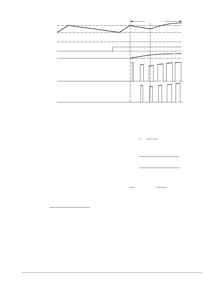
Line Under/Overvoltage Shutdown
The NCP1280 incorporates line undervoltage and
overvoltage shutdown (UV/OV) circuits. The under voltage
(UV) threshold is 1.52 V and the overvoltage threshold
(OV) is 3.61 V, for a ratio of 1:2.4. If the input voltage range
exceeds the pre-set OV threshold, the OV function can be
disabled by connecting a zener from this pin to ground. The
zener voltage should be less than 3.6 V.
The UV/OV circuit can be biased using an external
resistor divider from the input line. The resistor divider must
be sized to enable the controller once V
in
is within the
required operating range. If the UV or OV threshold is
reached, the soft start capacitor is discharged, and the
outputs are immediately disabled with no overlap delay as
shown in Figure 30. Also, if an UV condition is detected, the
5.0 V Reference Supply is disabled.
Figure 30. UV/OV Fault Timing Diagram
UV or OV Fault
OUT2
OUT1
0 V
0 V
0 V
0 V
V
OV
V
UV
UV/OV Voltage
V
AUX(off)
V
AUX(on)
V
AUX
Propagation delay to
outputs (t
UV
or t
OV
)
Once the UV or OV condition is removed and V
AUX
reaches 11 V, the controller initiates a soft start cycle.
Figure 31 shows the relationship between the UV/OV
voltage, the outputs and the soft start voltage.
The UV/OV pin can also be used to implement a remote
enable/disable function. Biasing the UV/OV pin below its
UV threshold disables the converter.
NCP1280
http://onsemi.com
13
Figure 31. Soft Start Timing Diagram (Using Auxiliary Winding)
V
AUX(off)
V
AUX(on)
V
AUX
0 V
0 V
2 V
0 V
0 V
0 V
OUT2
OUT1
Soft Start Voltage
UV/OV Voltage
SOFT START
Feedforward Ramp Generator
The NCP1280 incorporates line feedforward (FF) to
compensate for changes in line voltage. A FF Ramp
proportional to V
in
is generated and compared to V
EA
. If the
line voltage changes, the FF Ramp slope changes
accordingly. The duty cycle will be adjusted immediately
instead of waiting for the line voltage change to propagate
around the system and be reflected back on V
EA
.
A resistor between V
in
and the FF pin (R
FF
) sets the
feedforward current (I
FF
). The FF Ramp is generated by
charging an internal 10 pF capacitor (C
FF
) with a constant
current proportional to I
FF
. The FF Ramp is finished
(capacitor is discharged) once the Oscillator Ramp reaches
2.0 V. Please refer to Figure 2 for a functional drawing of the
Feedforward Ramp generator.
I
FF
is usually a few hundred microamps, depending on the
operating frequency and the required duty cycle. If the
operating frequency and maximum duty cycle are known,
I
FF
is calculated using the equation below:
IFF
+
CFF
VDC(inv)
125 k
W
6.7 k
W
ton(max)
where V
DC(inv)
is the voltage on the inverting input of the
Max DC Comparator and t
on(max)
is the maximum ON time.
Figure 18 shows the relationship between I
FF
and DC
MAX
.
For example, if a system is designed to operate at 200 kHz,
with a 60% maximum duty cycle at 100 V, the DC
MAX
pin
can be grounded and I
FF
is calculated as follows:
T
+
1
f
+
1
200 kHz
+
5.0
m
s
ton(max)
+
DCMAX
T
+
0.6
5.0
m
s
+
3.0
m
s
IFF
+
CFF
VDC(inv)
125 k
W
6.7 k
W
ton(max)
+
10 pF
0.888 V
125 k
W
6.7 k
W
3.0
m
s
+
55.2
m
A
For a minimum line voltage of 100 V, the required
feedforward resistor is calculated using the equation below:
RFF
+
Vin
IFF
*
12.0 k
W +
100 V
55.2
m
A
*
12.0 k
W [
1.82 M
W
From the above calculations it can be observed that I
FF
is
controlled predominantly by the value of R
FF
, as the
resistance seen into the FF pin is only 12 k
W. If a tight
maximum duty cycle control overtemperature is required,
R
FF
should have a low thermal coefficient.

NCP1280
http://onsemi.com
14
Current Limit
The NCP1280 has two overcurrent protection modes,
cycle by cycle and cycle skip. It allows the NCP1280 to
handle momentary and hard shorts differently for the best
tradeoff in performance and safety. The outputs are disabled
typically 90 ns after a current limit fault is detected.
The cycle by cycle mode terminates the conduction cycle
(reducing the duty cycle) if the voltage on the CS pin
exceeds 0.48 V. If the voltage on the CS pin exceeds 0.57 V,
the converter enters the cycle skip (CSKIP) mode. While in
the CSKIP mode, the soft start capacitor is discharged and
the converter is disabled by a time determined by the CSKIP
timer.
The CSKIP timer is set by immediately discharging the
capacitor on the CSKIP pin (C
CSKIP
), and then charging it
with a constant current source of 12.3
mA. The cycle skip
period ends when the voltage on the cycle skip capacitor
reaches 2.0 V. The cycle skip capacitor is calculated using
the equation below:
CCSKIP
[
TCSKIP
12.3
m
A
2 V
Using the above equation, a cycle skip period of 11.0
ms
requires a cycle skip capacitor of 68 pF. The differences
between the cycle by cycle and cycle skip modes are
observed in Figure 32.
Figure 32. Overcurrent Faults Timing Diagram
Cycle Skip
Voltage
0 V
0 V
0 V
0 V
0 V
OUT2
OUT1
I
LIM2
I
LIM1
V
AUX(off)
V
AUX(on)
V
AUX
CS Voltage
NORMAL
OPERATION
I
LIM2
RESET
I
LIM1
SOFT START
NORMAL
OPERATION
T
CSKIP
Once the cycle skip period is complete and V
AUX
reaches
11 V, a soft start sequence commences. The possible
minimum OFF time is set by C
CSKIP
. However, the actual
OFF time is generally greater than C
CSKIP
because it is the
cycle skip period added to the time it takes V
AUX
to reach
11 V.
Oscillator
The NCP1280 oscillator frequency is set by a single
external resistor connected between the R
T
pin and GND.
The oscillator is designed to operate up to 500 kHz.
The voltage on the R
T
pin is laser trim adjusted during
manufacturing to 1.3 V for an R
T
of 101 k
W. A current set
by R
T
generates an Oscillator Ramp by charging an internal
10 pF capacitor as shown in Figure 2. The period ends
(capacitor is discharged) once the Oscillator Ramp reaches
2.0 V. If R
T
increases, the current and the Oscillator Ramp
slope decrease, thus reducing the frequency. If R
T
decreases,
the opposite effect is obtained. Figure 16 shows the
relationship between R
T
and the oscillator frequency.
NCP1280
http://onsemi.com
15
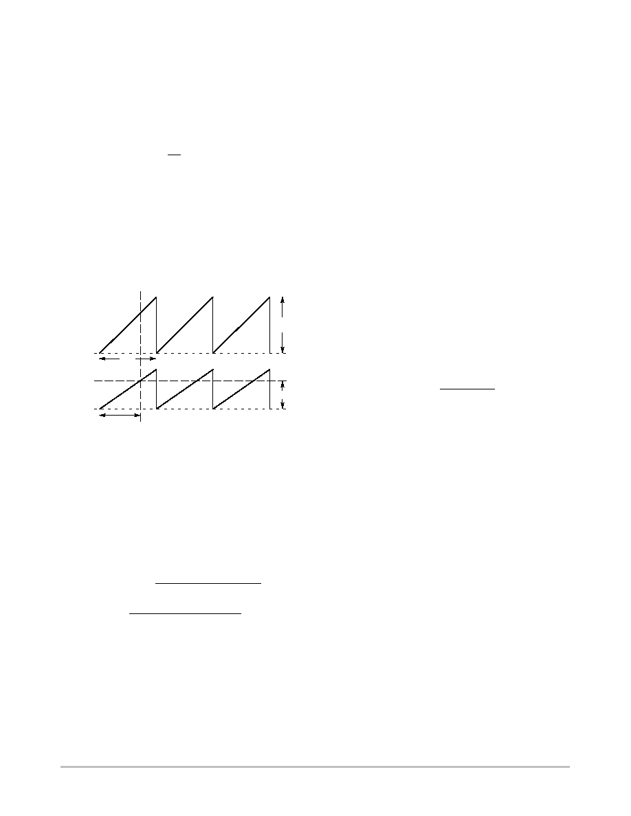
Maximum Duty Cycle
A dedicated internal comparator limits the maximum ON
time of OUT1 by comparing the FF Ramp to V
DC(inv)
. If the
FF Ramp voltage exceeds V
DC(inv)
, the output of the Max
DC Comparator goes high.
This will reset the Output Latch,
thus turning OFF the outputs and limiting the duty cycle.
Duty cycle is defined as:
DC
+
ton
T
+
ton
f
Therefore, the maximum ON time can be set to yield the
desired DC if the operating frequency is known. The
maximum ON time is set by adjusting the FF Ramp to reach
V
DC(inv)
in a time equal to t
on(max)
as shown in Figure 33.
The maximum ON time should be set for the minimum line
voltage. As line voltage increases, the slope of the FF Ramp
increases. This reduces the duty cycle below DC
MAX
, which
is a desirable feature as the duty cycle is inversely
proportional to line voltage.
Figure 33. Maximum ON Time Limit Waveforms
Oscillator Ramp
0 V
0 V
FF Ramp
T
t
on(max)
V
DC(inv)
2 V
An internal resistor divider from a 2.0 V reference is used
to set V
DC(inv)
. If the DC
MAX
pin is grounded, V
DC(inv)
is
0.88 V. If the pin is floating, V
DC(inv)
is 1.19 V. This is
equivalent to 60% or 80% of a 1.5 V FF Ramp. V
DC(inv)
can
be adjusted to other values by using an external resistor
network on the DC
MAX
pin. For example, if the minimum
line voltage is 100 V, R
FF
is 1.82 M
W, operating frequency
is 200 kHz and a maximum duty cycle of 70% is required,
V
DC(inv)
is calculated as follows:
VDC(inv)
+
IFF
6.7 k
W
ton(max)
CFF
125 k
W
VDC(inv)
+
55.2
m
A
6.7 k
W
3.5
m
s
10 pF
125 k
W
+
1.04 V
This can be achieved by connecting a 19.6 k
W resistor
from the DC
MAX
pin to GND. The maximum duty cycle
limit can be disabled connecting a 100 k
W resistor between
the DC
MAX
and V
REF
pins.
5.0 V Reference
The NCP1280 includes a precision 5.0 V reference output.
The reference output is biased directly from V
AUX
and it can
supply up to 6 mA. Load regulation is 50 mV and line
regulation is 100 mV over the complete operating range.
It is recommended to bypass the reference output with a
0.1
mF ceramic capacitor. The reference output is disabled
when an UV fault is present.
PWM Comparator
In steady state operation, the PWM comparator adjusts the
duty cycle by comparing the error signal to the FF Ramp.
The error signal is fed into the V
EA
input. The V
EA
input can
be driven directly with an optocoupler and a pull-up resistor
from V
REF
. The drive of the V
EA
pin is simplified by
internally incorporating a series diode and resistor. The
series diode provides a 0.7 V offset between V
EA
input and
the PWM comparator inverting input. The outputs are
enabled if the V
EA
voltage is approximately 0.7 above the
valley voltage of the FF Ramp.
The pull-up resistor is selected such that in the absense of
the error signal, the voltage on the V
EA
pin exceeds the peak
amplitude of the FF Ramp. Otherwise, the converter will not
be able to reach maximum duty cycle. The V
EA
range
required to control the DC from 0% to DC
MAX
is given by
the equation below:
VEA(L)
t
VEA
t
IFF
DC
186.56 pf
f )
VEA(L)
where, V
EA(L)
is the PWM comparator lower input
threshold.
Soft Start
Soft start (SS) allows the converter to gradually reach
steady state operation, thus reducing start-up stress and
surges on the system. The duty cycle is limited during a soft
start sequence by comparing the Oscillator Ramp to the SS
voltage (V
SS
) by means of the Soft Start Comparator.
A 6.2
mA current source starts to charge the capacitor on
the SS pin once faults are removed and V
AUX
reaches 11 V.
The Soft Start Comparator controls the duty cycle while the
SS voltage is below 2.0 V. Once V
SS
reaches 2.0 V, it exceeds
the Oscillator Ramp voltage and the Soft Start Comparator
does not limit the duty cycle. Figure 34 shows the
relationship between the outputs duty cycle and the soft start
voltage.

NCP1280
http://onsemi.com
16
Figure 34. Soft Start Timing Diagram
OUT1
OUT2
V
SS
Oscillator
Ramp
If the soft start period is too long, V
AUX
will discharge to
7 V before the converter output is completely in regulation
causing the outputs to be disabled. If the converter output is
not completely discharged when the outputs are re-enabled,
the converter will eventually reach regulation exhibiting a
non-monotonic start-up behavior. But, if the converter
output is completely discharged when the outputs are
re-enabled, the cycle may repeat and the converter will not
start.
In the event of an UV, OV, or cycle skip fault, the soft start
capacitor is discharged. Once the fault is removed, a soft
start cycle commences. The soft start steady state voltage is
approximately 4.1 V.
Control Outputs
The NCP1280 has two in-phase control outputs, OUT1
and OUT2, with adjustable overlap delay (t
D
). OUT2
precedes OUT1 during a low to high transition and OUT1
precedes OUT2 at any high to low transition. Figure 35
shows the relationship between OUT1 and OUT2.
Figure 35. Control Outputs Timing Diagram
t
D
(Trailing)
t
D
(Leading)
OUT1
OUT2
Generally, OUT1 controls the main switching element.
Output 2, once inverted, can control a synchronous rectifier.
The overlap delay prevents simultaneous conduction.
Output 2 can also be used to control an active clamp reset.
Once V
AUX
reaches 11 V, the internal start-up circuit is
disabled and the One Shot Pulse Generator is enabled. If no
faults are present, the outputs turn ON. Otherwise, the
outputs remain OFF until the fault is removed and V
AUX
reaches 11 V again.
The control outputs are biased from V
AUX
. The outputs
can supply up to 10 mA each and their high state voltage is
usually 0.2 V below V
AUX
. Therefore, the auxiliary supply
voltage should not exceed the maximum input voltage of the
driver stage.
If the control outputs need to drive a large capacitive load,
a driver should be used between the NCP1280 and the load.
ON Semiconductor's MC33152 is a good selection for an
integrated driver. Figures 27 and 28 shows the relationship
between the output's rise and fall times vs capacitive load.
Time Delay
The overlap delay between the outputs is set connecting
a resistor (R
D
) between the t
D
and V
REF
pins. A minimum
overlap delay of 80 ns is obtained when R
D
is 60 k
W. If R
D
is not present, the delay is 200 ns.
The output duty cycle can be adjusted from 0% to 85%
selecting appropriate values of R
FF
and V
DC(inv)
. It should
be noted that the overlap delay may cause OUT2 to reach
100% duty cycle. Therefore, if OUT2 is used, the maximum
duty cycle of OUT2 needs to be kept below 100%. The
maximum overlap delay, t
D(max)
, depends on the maximum
duty cycle and frequency of operation. The maximum
overlap delay is calculated using the equation below.
tD(max)
v
(1
*
DC)
2
For example, if the converter operates at a frequency of
300 kHz with a maximum duty cycle of 80%, the maximum
allowed overlap delay is 333 ns. However, this is a
theoretical limit and variations over the complete operating
range should be considered when selecting the overlap
delay.
NCP1280
http://onsemi.com
17
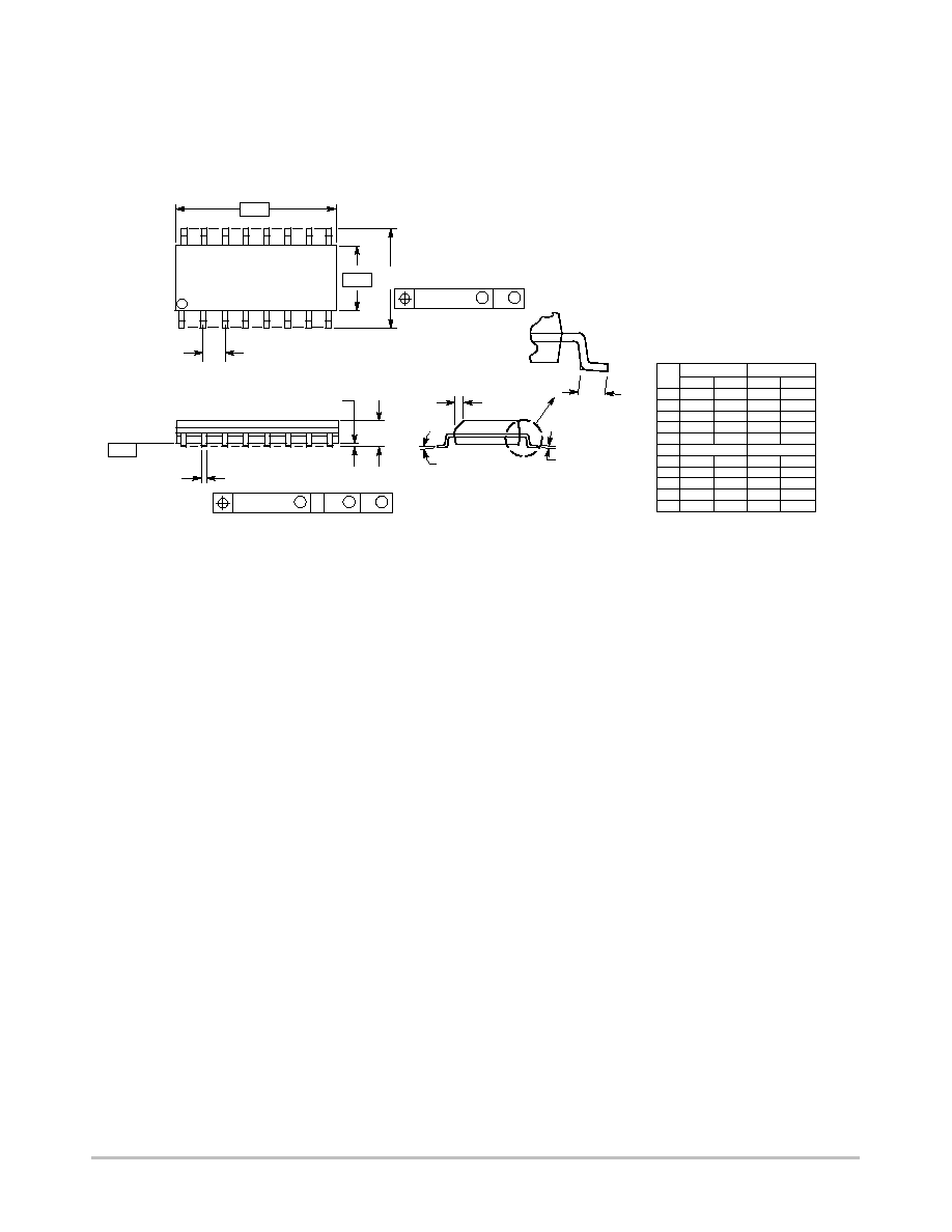
PACKAGE DIMENSIONS
SO-16
D SUFFIX
CASE 751B-05
ISSUE J
NOTES:
1. DIMENSIONING AND TOLERANCING PER ANSI
Y14.5M, 1982.
2. CONTROLLING DIMENSION: MILLIMETER.
3. DIMENSIONS A AND B DO NOT INCLUDE
MOLD PROTRUSION.
4. MAXIMUM MOLD PROTRUSION 0.15 (0.006)
PER SIDE.
5. DIMENSION D DOES NOT INCLUDE DAMBAR
PROTRUSION. ALLOWABLE DAMBAR
PROTRUSION SHALL BE 0.127 (0.005) TOTAL
IN EXCESS OF THE D DIMENSION AT
MAXIMUM MATERIAL CONDITION.
1
8
16
9
SEATING
PLANE
F
J
M
R
X 45
_
G
8 PL
P
-B-
-A-
M
0.25 (0.010)
B
S
-T-
D
K
C
16 PL
S
B
M
0.25 (0.010)
A
S
T
DIM
MIN
MAX
MIN
MAX
INCHES
MILLIMETERS
A
9.80
10.00
0.386
0.393
B
3.80
4.00
0.150
0.157
C
1.35
1.75
0.054
0.068
D
0.35
0.49
0.014
0.019
F
0.40
1.25
0.016
0.049
G
1.27 BSC
0.050 BSC
J
0.19
0.25
0.008
0.009
K
0.10
0.25
0.004
0.009
M
0
7
0
7
P
5.80
6.20
0.229
0.244
R
0.25
0.50
0.010
0.019
_
_
_
_

NCP1280
http://onsemi.com
18
ON Semiconductor and are registered trademarks of Semiconductor Components Industries, LLC (SCILLC). SCILLC reserves the right to make changes without further notice
to any products herein. SCILLC makes no warranty, representation or guarantee regarding the suitability of its products for any particular purpose, nor does SCILLC assume any liability
arising out of the application or use of any product or circuit, and specifically disclaims any and all liability, including without limitation special, consequential or incidental damages.
"Typical" parameters which may be provided in SCILLC data sheets and/or specifications can and do vary in different applications and actual performance may vary over time. All
operating parameters, including "Typicals" must be validated for each customer application by customer's technical experts. SCILLC does not convey any license under its patent rights
nor the rights of others. SCILLC products are not designed, intended, or authorized for use as components in systems intended for surgical implant into the body, or other applications
intended to support or sustain life, or for any other application in which the failure of the SCILLC product could create a situation where personal injury or death may occur. Should
Buyer purchase or use SCILLC products for any such unintended or unauthorized application, Buyer shall indemnify and hold SCILLC and its officers, employees, subsidiaries, affiliates,
and distributors harmless against all claims, costs, damages, and expenses, and reasonable attorney fees arising out of, directly or indirectly, any claim of personal injury or death
associated with such unintended or unauthorized use, even if such claim alleges that SCILLC was negligent regarding the design or manufacture of the part. SCILLC is an Equal
Opportunity/Affirmative Action Employer. This literature is subject to all applicable copyright laws and is not for resale in any manner.
PUBLICATION ORDERING INFORMATION
N. American Technical Support: 800-282-9855 Toll Free
USA/Canada
Japan: ON Semiconductor, Japan Customer Focus Center
2-9-1 Kamimeguro, Meguro-ku, Tokyo, Japan 153-0051
Phone: 81-3-5773-3850
NCP1280/D
The product described herein (NCP1280) may be covered by one or more U.S. patents. There may be other patents pending.
LITERATURE FULFILLMENT:
Literature Distribution Center for ON Semiconductor
P.O. Box 5163, Denver, Colorado 80217 USA
Phone: 303-675-2175 or 800-344-3860 Toll Free USA/Canada
Fax: 303-675-2176 or 800-344-3867 Toll Free USA/Canada
Email: orderlit@onsemi.com
ON Semiconductor Website: http://onsemi.com
Order Literature: http://www.onsemi.com/litorder
For additional information, please contact your
local Sales Representative.