 | –≠–ª–µ–∫—Ç—Ä–æ–Ω–Ω—ã–π –∫–æ–º–ø–æ–Ω–µ–Ω—Ç: NCP1337PG | –°–∫–∞—á–∞—Ç—å:  PDF PDF  ZIP ZIP |
©
Semiconductor Components Industries, LLC, 2005
October, 2005 - Rev. P0
1
Publication Order Number:
NCP1337/D
NCP1337
PWM Current-Mode
Controller for Free Running
Quasi-Resonant Operation
The NCP1337 combines a true current mode modulator and a
demagnetization detector which ensures full Borderline/Critical
Conduction Mode in any load/line conditions together with
minimum drain voltage switching (Quasi-Resonant operation). The
transformer core reset detection is done internally, without using any
external signal, due to the Soxyless concept. The frequency is
internally limited to 130 kHz, preventing the controller to operate
above the 150 kHz CISPR-22 EMI starting limit.
By monitoring the feedback pin activity, the controller enters
ripple mode as soon as the power demand falls below a
predetermined level. As each restart is softened by an internal
soft-start, and as the frequency cannot go below 25 kHz, no audible
noise can be heard.
The NCP1337 also features an efficient protective circuitry which,
in presence of an overcurrent condition, disables the output pulses
and enters a safe burst mode, trying to restart. Once the default has
gone, the device auto-recovers. Also included is a bulk voltage
monitoring function (known as brown-out protection), an adjustable
overpower compensation, and a V
CC
OVP. Finally, an internal 4.0 ms
soft-start eliminates the traditional startup stress.
Features
∑
Free-Running Borderline/Critical Mode Quasi-Resonant Operation
∑
Current-Mode
∑
Soft Ripple Mode with Minimum Switching Frequency for Standby
∑
Auto-Recovery Short-Circuit Protection Independent of Auxiliary
Voltage
∑
Overvoltage Protection
∑
Brown-Out Protection
∑
Two Externally Triggerable Fault Comparators (one for a disable
function, and the other for a permanent latch)
∑
Internal 4.0 ms Soft-Start
∑
500 mA Peak Current Drive Sink Capability
∑
130 kHz Max Frequency
∑
Internal Leading Edge Blanking
∑
Internal Temperature Shutdown
∑
Direct Optocoupler Connection
∑
Dynamic Self-Supply with Levels of 12 V (On) and 10 V (Off)
∑
SPICE Models Available for TRANsient and AC Analysis
∑
These are Pb-Free Devices*
Typical Applications
∑
AC-DC Adapters for Notebooks, etc.
∑
Offline Battery Chargers
∑
Consumer Electronics (DVD Players, Set-Top Boxes, TVs, etc.)
∑
Auxiliary Power Supplies (USB, Appliances, TVs, etc.)
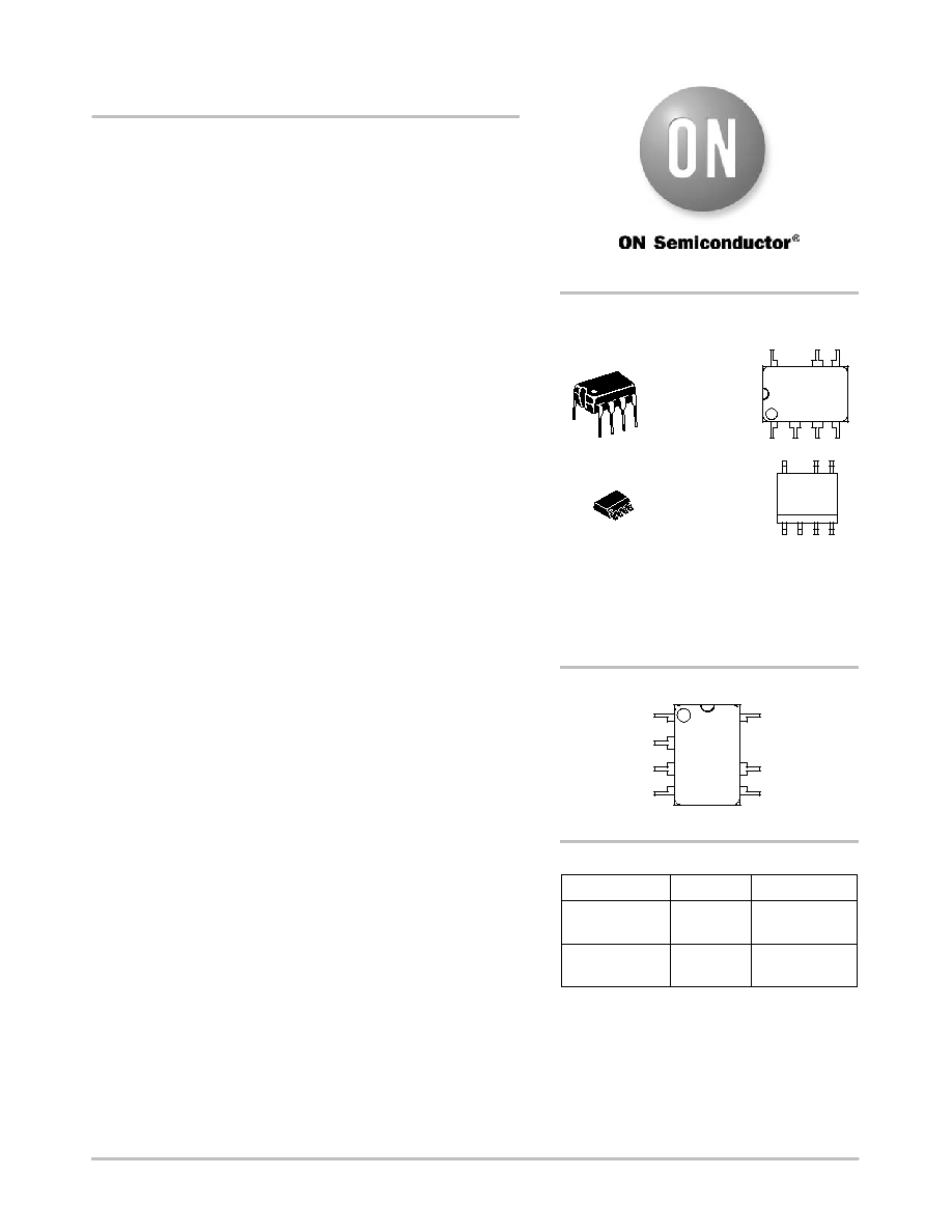
PDIP-7
P SUFFIX
CASE 626B
PIN CONNECTIONS
Device
Package
Shipping
ORDERING INFORMATION
NCP1337PG
PDIP-7
(Pb-Free)
50 Units/Tube
http://onsemi.com
MARKING
DIAGRAM
A
= Assembly Location
WL
= Wafer Lot
Y, YY
= Year
WW
= Work Week
G
= Pb-Free Package
G
= Pb-Free Package
(Top View)
FB
BO
CS
GND
DRV
HV
VCC
NCP1337P
AWL
YYWWG
1
SOIC-7
D SUFFIX
CASE 751U
NCP1337DR2G
SOIC-7
(Pb-Free)
2500 Tape & Reel
For information on tape and reel specifications,
including part orientation and tape sizes, please
refer to our Tape and Reel Packaging Specification
Brochure, BRD8011/D.
*For additional information on our Pb-Free strategy
and soldering details, please download the
ON Semiconductor Soldering and Mounting
Techniques Reference Manual, SOLDERRM/D.
1
2
3
4
8
6
5
P1337
AYWW
G
1
8

NCP1337
http://onsemi.com
2
PIN FUNCTION DESCRIPTION
Pin No.
Symbol
Function
Description
1
BO
Brown-out and external
triggering
∑
By connecting this pin to the input voltage through a resistor divider, the
controller ensures operation at a safe mains level.
∑
If an external event brings this pin above 3.0 V, the controller's output is
disabled.
∑
If an external event brings this pin above 5.0 V, the controller is
permanently latched-off.
2
FB
Sets the peak current
setpoint
∑
By connecting an optocoupler or an auxiliary winding to this pin, the peak
current setpoint is adjusted accordingly to the output power demand.
∑
When the requested peak current setpoint is below the internal standby
level, the device enters soft ripple mode.
3
CS
Current sense input and
overpower compensation
adjustment
∑
This pin senses the primary current and routes it to the internal comparator
via an L.E.B.
∑
Inserting a resistor in series with the pin allows to control the overpower
compensation level.
4
GND
IC ground
5
DRV
Output driver
∑
To be connected to an external MOSFET.
6
VCC
IC supply
∑
Connected to a tank capacitor (and possibly an auxiliary winding).
∑
When V
CC
reaches 18.6 V, an internal OVP stops the output pulses.
8
HV
High-voltage pin
∑
Connected to the high-voltage rail, this pin injects a constant current into
the V
CC
bulk capacitor and ensures a clean lossless startup sequence.
1
8
2
3
4
6
5
NCP1337
Rcomp
BO
+
C
bulk
+
V
CC
V
CC
+
V
OUT
Figure 1. Typical Application Schematic
NCP1337
http://onsemi.com
3
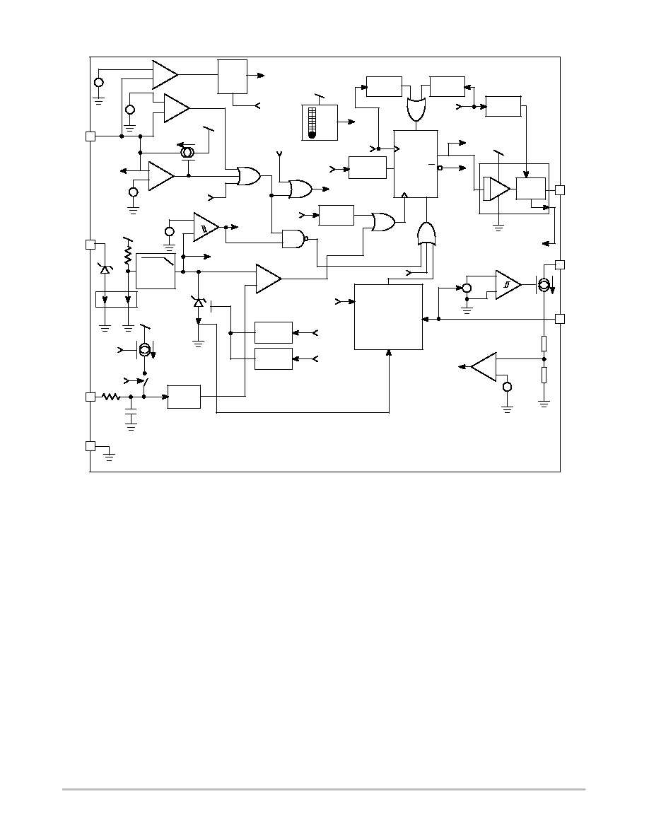
Figure 2. Internal Circuit Architecture
+
GND
BO
5 V
+
-
+
3 V
DISABLE
10
m
A
Vdd
+
-
BOK
7.5
m
s min
period
SStart
Ton
Clk
D
R1
R2
Q
Q
S
Soxyless
demag
detection
DRV
Startup
S
Q
R
V
CC
< 4 V
PERM. LATCH
Vdd
TSD
TSD
Soxyless
8
m
s
timeout
35
m
s
max Toff
5.5
m
s
blanking
Toff
V
CC
Soxyless
V
BO
+
500 mV
OVP
+
-
SSkip
Skip
Setpoint
+
-
+
-
20 kHz
Low-pass
filter
Vdd
FB
3 V
500 mV
FAULT
if Zener
activated
Vdd
Ton
V
BO
70
m
A x V
BO
- 35
m
A
CS
2 p
4 k
350 ns
LEB
CS
comp.
300
m
s
soft-skip
SSkip
4 ms
soft-start
SStart
PERM.
LATCH
67
m
s
max Ton
FAULT
Management*
FAULT
(*If FAULT duration > 80 ms = > STOP
Restart when 2nd time VCC = VCCon)
TSD
Inhib
Toff
Ton
+
-
+
12 V
10 V
5 V
HV
9.5 mA or
600
mA
VCC
+
-
+
OVP
18.6 V
100 mV
130 mV
+
Ton

NCP1337
http://onsemi.com
4
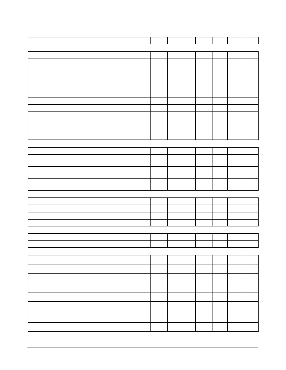
MAXIMUM RATINGS
Rating
Symbol
Value
Unit
Voltage on Pin 8 (HV) when Pin 6 (V
CC
) is Decoupled to Ground with 10
m
F
V
HV
-0.3 to 500
V
Maximum Current in Pin 8 (HV)
-
20
mA
Power Supply Voltage, Pin 6 (V
CC
) and Pin 5 (DRV)
V
CCmax
-0.3 to 20
V
Maximum Current in Pin 6 (V
CC
)
-
"
30
mA
Maximum Voltage on all Pins except Pin 8 (HV), Pin 6 (V
CC
) and Pin 5 (DRV)
-
-0.3 to 10
V
Maximum Current into all Pins except Pin 8 (HV), Pin 6 (V
CC
) and Pin 5 (DRV)
-
"
10
mA
Maximum Current into Pin 6 (DRV) during ON Time and T
BLANK
-
"
1.0
A
Maximum Current into Pin 6 (DRV) after T
BLANK
during OFF Time
-
"
15
mA
Thermal Resistance, Junction-to-Case
R
q
JC
57
∞
C/W
Thermal Resistance, Junction-to-Air, SOIC Version
R
q
JA
178
∞
C/W
Thermal Resistance, Junction-to-Air, DIP Version
R
q
JA
100
∞
C/W
Maximum Junction Temperature
TJ
MAX
150
∞
C
Operating Temperature Range
-
-40 to +125
∞
C
Storage Temperature Range
-
-60 to +150
∞
C
ESD Capability, HBM Model per Mil-std-883, Method 3015 (All Pins except HV)
-
2.0
kV
ESD Capability, Machine Model
-
200
V
Maximum ratings are those values beyond which device damage can occur. Maximum ratings applied to the device are individual stress limit values
(not normal operating conditions) and are not valid simultaneously. If these limits are exceeded, device functional operation is not implied, damage
may occur and reliability may be affected.
1. This device contains latchup protection and exceeds 100 mA per JEDEC standard JESD78.
NCP1337
http://onsemi.com
5
ELECTRICAL CHARACTERISTICS
(For typical values T
J
= 25
∞
C, for min/max values T
J
= 0
∞
C to +125
∞
C, Max T
J
= 150
∞
C,
V
CC
= 11 V, unless otherwise noted.)
Characteristic
Pin
Symbol
Min
Typ
Max
Unit
SUPPLY SECTION
V
CC
Increasing Level at which the Controller Starts
6
VCC
ON
11
12
13
V
V
CC
Decreasing Level at which the Controller Stops
6
VCC
MIN
9.0
10
11
V
Protection Mode is Activated if V
CC
reaches this Level whereas the HV
Current Source is ON
6
VCC
OFF
-
9.0
-
V
V
CC
Decreasing Level at which the Latch-Off Phase Ends
6
VCC
LATCH
3.6
5.0
6.0
V
Margin between V
CC
Level at which Latch Fault is Released and
VCC
LATCH
-
V
MARGIN
0.3
-
-
V
V
CC
Increasing Level at which the Controller Enters Protection Mode
6
VCC
OVP
17.6
18.6
19.6
V
V
CC
Level below which HV Current Source is Reduced
6
VCC
INHIB
-
1.5
-
V
Internal IC Consumption, No Output Load on Pin 5, F
SW
= 60 kHz
6
ICC1
-
1.2
-
mA
Internal IC Consumption, 1.0 nF Output Load on Pin 5, F
SW
= 60 kHz
6
ICC2
-
2.0
-
mA
Internal IC Consumption, Latch-Off Phase, V
CC
= 8.0 V
6
ICC3
-
600
-
m
A
Internal IC Consumption in Skip
6
ICC
LOW
-
600
-
m
A
INTERNAL STARTUP CURRENT SOURCE
Minimum Guaranteed Startup Voltage on HV Pin
8
V
HVmin
-
-
55
V
High-Voltage Current Source when V
CC
> VCC
INHIB
(V
CC
= 10.5 V, V
HV
= 60 V)
8
IC1
5.5
9.5
15
mA
High-Voltage Current Source when V
CC
< VCC
INHIB
(V
CC
= 0 V, V
HV
= 60 V)
8
IC2
0.3
0.6
1.1
mA
Leakage Current Flowing when the HV Current Source is OFF
(V
CC
= 17 V, V
HV
= 500 V)
8
I
HVLeak
-
-
90
m
A
DRIVE OUTPUT
Output Voltage Rise-Time @ CL = 1.0 nF, 10-90% of Output Signal
5
T
R
-
50
-
ns
Output Voltage Fall-Time @ CL = 1.0 nF, 10-90% of Output Signal
5
T
F
-
20
-
ns
Source Resistance
5
R
OH
-
20
-
W
Sink Resistance
5
R
OL
-
8.0
-
W
TEMPERATURE SHUTDOWN
Temperature Shutdown
-
TSD
130
-
-
∞
C
Hysteresis on Temperature Shutdown
-
-
-
30
-
∞
C
CURRENT COMPARATOR
Maximum Internal Current Setpoint (@ I
FB
= I
FB100%
)
3
V
CSLimit
475
500
525
mV
Minimum Internal Current Setpoint (@ I
FB
= I
FBrippleIN
)
3
V
CSrippleIN
-
100
-
mV
Internal Current Setpoint for I
FB
= I
FBrippleOUT
3
V
CSrippleOUT
-
130
-
mV
Propagation Delay from Current Detection to Gate OFF State
3
T
DEL
-
120
150
ns
Leading Edge Blanking Duration
3
T
LEB
-
350
-
ns
Internal Current Offset Injected on the CS Pin during ON Time
(Over Power Compensation)
@ 1.0 V on Pin 1 and Vpin3 = 0.5 V
@ 2.0 V on Pin 1 and Vpin3 = 0.5 V
3
I
OPC
-
-
35
105
-
-
m
A
Maximum ON Time
5
MaxT
ON
52
67
82
m
s

NCP1337
http://onsemi.com
6
ELECTRICAL CHARACTERISTICS
(continued) (For typical values T
J
= 25
∞
C, for min/max values T
J
= 0
∞
C to +125
∞
C,
Max T
J
= 150
∞
C, V
CC
= 11 V, unless otherwise noted.)
Characteristic
Pin
Symbol
Min
Typ
Max
Unit
FEEDBACK SECTION
FB Current under which FAULT is Detected
2
I
FBopen
-
40
-
m
A
FB Current for which Internal Setpoint is 100%
2
I
FB100%
-
50
-
m
A
FB Current above which DRV Pulses are Stopped
2
I
FBrippleIN
-
220
-
m
A
FB Current under which DRV Pulses are Reauthorized after having
reached I
FBrippleIN
2
I
FBrippleOUT
-
205
-
m
A
FB Current above which FB Pin Voltage is not Regulated anymore
2
I
FBregMax
-
500
-
m
A
FB Pin Voltage when I
FBopen
< I
FB
< I
FBregMax
2
V
FB
2.8
3.0
3.2
V
Duration before Entering Protection Mode after FAULT Detection
-
T
FAULT
-
80
-
ms
Internal Soft-Start Duration (Up to V
CSLimit
)
-
T
SS
-
4.0
-
ms
Internal Soft-Skip Duration (Up to V
CSLimit
)
-
T
SSkip
-
300
-
m
s
BROWN-OUT AND LATCH SECTION
Brown-Out Detection Level
1
V
BO
460
500
540
mV
Current Flowing out of Pin 1 when Brown-Out Comparator has Toggled
1
I
BO
-
10
-
m
A
Vpin1 Threshold that Disables the Output
1
V
DISABLE
2.8
3.0
3.3
V
Vpin1 Threshold that Activates the Permanent Latch
1
V
LATCH
4.75
5.0
5.25
V
DEMAGNETIZATION DETECTION BLOCK
Current Threshold for Demagnetization Detection
5
I
SOXYth
-
210
-
m
A
Max Voltage on DRV Pin During OFF Time after T
BLANK
(when Sinking 15 mA)
5
V
DRVlowMAX
-
-
1.5
V
Min Voltage on DRV Pin During OFF Time after T
BLANK
(when Sourcing 15 mA)
5
V
DRVlowMIN
-0.6
-
-
V
Propagation Delay from Demag Detection to Gate ON State
(I
GATE
Slope of 500 A/s)
5
T
DMG
-
180
220
ns
Blanking Window after Gate OFF State before Detecting
Demagnetization
5
T
BLANK
-
5.5
-
m
s
Timeout on Demag Signal
5
T
OUT
-
8.0
-
m
s
Maximum OFF Time
5
MaxT
OFF
-
35
42
m
s
Minimum Switching Period
5
MinPeriod
6.8
7.5
8.2
m
s

NCP1337
http://onsemi.com
7
APPLICATION INFORMATION
INTRODUCTION
The NCP1337 implements a standard current mode
architecture where the switch-off time is dictated by the
peak current setpoint, whereas the core-reset detection
triggers the turn-on event. This component represents
the ideal candidate where low part-count is the key
parameter, particularly in low-cost AC-DC adapters,
consumer electronics, auxiliary supplies, etc. Due to
its high-performance, high-voltage technology, the
NCP1337 incorporates all the necessary features needed to
build a rugged and reliable Switch-Mode Power Supply
(SMPS):
∑
Quasi-Resonant Operation: Valley-switching
operation is ensured whatever the operating conditions
are, due to the internal soxyless circuitry. As a result,
there are virtually no primary switch turn-on losses,
and no secondary diode recovery losses, and EMI and
video noise perturbations are reduced. The converter
also stays a first-order system and accordingly eases
the feedback loop design.
∑
Dynamic Self-Supply (DSS): Due to its Very High
Voltage Integrated Circuit (VHVIC) technology,
ON Semiconductor's NCP1337 allows for a direct pin
connection to the high-voltage DC rail. A dynamic
current source charges up a capacitor and thus
provides a fully independent V
CC
level. As a result,
low power applications will not require any auxiliary
winding to supply the controller. In applications
where this winding is anyway required (see "Power
Dissipation" section in the application note), the DSS
will simplify the V
CC
capacitor selection.
∑
Overcurrent Protection (OCP): When the feedback
current is below minimum value, a fault is detected. If
this fault is present for more than 80 ms, NCP1337
enters an auto-recovery soft burst mode. All pulses are
stopped and the V
CC
capacitor discharges down to
5.0 V. Then, by monitoring the V
CC
level, the startup
current source is activated ON and OFF to create a
burst mode. After the current source being activated
twice, the controller tries to restart, with a 4.0 ms
soft-start. If the fault has gone, the SMPS resumes
operation. If the fault is still there, the burst sequence
starts again. The soft-start, together with a minimum
frequency clamp, allow to reduce the noise generated
in the transformer in short-circuit conditions.
∑
Overvoltage Protection (OVP): By continuously
monitoring the V
CC
voltage level, the NCP1337 stops
switching whenever an overvoltage condition is
detected.
∑
Brown-Out Detection (BO): By monitoring the level
on Pin 1 during normal operation, the controller
protects the SMPS against low mains condition. When
Pin 1 level falls below 500 mV, the controller stops
pulsing until this level goes back and resumes
operation. By adjusting the resistor divider connected
between the high input voltage and this pin, start and
stop levels are programmable.
∑
Over Power Compensation (OPC): An internal
current source injects out of Pin 3 (CS pin) a current
proportional to the voltage applied on Pin 1. As this
voltage is an image of the input voltage, by inserting a
resistor in series with Pin 3, it is possible to create an
offset on the current sense signal that will compensate
the effect of the input voltage variation.
∑
External Latch Trip Point: By externally forcing a
level on Pin 1 (e.g., with a signal coming from a
temperature sensor) greater than 3.0 V (but below
5.0 V), it is possible to disable the output of the
controller. If the voltage is forced over 5.0 V, the
controller is permanently latched-off: to resume
normal operation, the V
CC
voltage should go below
4.0 V, which implies to unplug the SMPS from the
mains.
∑
Standby Ability: Under low load conditions,
NCP1337 enters a soft ripple mode: when the CS
setpoint becomes lower than 20% of the maximum
peak current, output pulses are stopped, then switching
is starting again when FB loop forces a setpoint higher
than 25%. As this occurs at low peak current, with
soft-skip activated, and as the T
OFF
is clamped,
noise-free operation is guaranteed, even with a cheap
transformer.

NCP1337
http://onsemi.com
8
V
CC
CS
Setpoint
CS
FAULT
TIMER
80 ms
VCC
ON
VCC
MIN
Fault
V
CSstby
V
CSLimit
SS
When FAULT is activated,
the 80 ms timer starts.
At startup, a 4.0 ms soft-start is activated.
If the current Setpoint is above the fault
level, FAULT flag is raised.
When the timer ends, if FAULT is not activated
anymore, the controller works normally.
Timing Diagrams
Figure 3. Startup Sequence

NCP1337
http://onsemi.com
9
V
CC
CS
Setpoint
CS
FAULT
TIMER
80 ms
VCC
ON
VCC
MIN
Fault
V
CSLimit
SS
VCC
LATCH
Restart on 2
nd
cycle
When the current setpoint rises above
fault level, FAULT flag is activated.
When FAULT flag
is activated, timer
is restarted.
Overload
Overload is removed here
Output pulses
are stopped.
80 ms Fault Timer
Normal Startup
Figure 4. Overload

NCP1337
http://onsemi.com
10
VCS
rippleOUT
VCS
rippleIN
CS
(envelope)
Min T
ON
CS
Setpoint
VCC
min
VCC
on
VCC
Soft-start on
each re-start
Figure 5. Soft Ripple Mode in Standby

NCP1337
http://onsemi.com
11
Soxyless
The "Valley point detection" is based on the observation
of the Power MOSFET Drain voltage variations. When the
transformer is fully demagnetized, the Drain voltage
evolution from the plateau level down to the V
IN
asymptote
is governed by the resonating energy transfer between the
L
P
transformer inductor and the global capacitance present
on the Drain. These voltage oscillations create current
oscillation in the parasitic capacitor across the switching
MOSFET (modelized by the Crss capacitance between
Gate and Drain): a negative current (flowing out of DRV
pin) takes place during the decreasing part of the Drain
oscillation, and a positive current (entering into the DRV
pin) during the increasing part.
The Drain valley corresponds to the inversion of the
current (i.e., the zero crossing): by detecting this point, we
always ensure a true valley turn-on.
Lprim
Crss
DRV
Isoxy
Vswitch
T
SWING
t
Figure 6. Soxyless Concept
The current in the Power MOSFET gate is:
Igate = Vringing/Zc (with Zc the capacitance impedance)
so
Igate = Vringing
S (2 S p S Fres S Crss)
The magnitude of this gate current depends on the
MOSFET, the resonating frequency and the voltage swing
present on the Drain at the end of the plateau voltage.
The dead time T
SWING
is given by the equation:
Tswing
+
0.5 Fres
+ p
* Lp * Cdrain
(eq. 1)
(where L
P
is the primary transformer inductance and
C
DRAIN
the total capacitance present on the MOSFET
Drain. This capacitance includes the snubber capacitor if
any, the transformer windings stray capacitance plus the
parasitic MOSFET capacitances C
OSS
and C
RSS
).
Internal Feedback Circuitry
To simplify the implementation of a primary regulation,
it is necessary to inject a current into the FB pin (instead of
sourcing it out). But to have a precise primary regulation,
the voltage present on FB pin must be regulated. Figure 8
gives the FB pin internal implementation: the circuitry
combines the functions of a current to voltage converter
and a voltage regulator.
FB
+
-
+
3 V
Vdd
Internal
Setpoint
20 kHz
Low-pass Filter
Figure 7. Internal Implementation of FB Pin

NCP1337
http://onsemi.com
12
The input information is the current injected in FB pin by
the feedback loop. The range of current is from 40
mA for
overload detection to 220
mA corresponding to V
CSrippleIN
.
In transients, currents from 0 to more than 400
mA may also
appear: the circuitry is able to sustain them.
To regulate the FB pin voltage, the operational amplifier
needs to have a high gain and a wide bandwidth. But the
feedback information used internally needs to be filtered,
because we don't want the controller to be sensitive to the
switching noise. For this purpose, a 20 kHz filter is added
after the shunt regulator, and any reading of the feedback
signal (for ripple mode, fault detection, or setpoint
elaboration) is done after.
Soft Burst Mode (Protection Mode)
The NCP1337 features a fault timer to detect an overload
completely independently of the V
CC
voltage. As soon as
the feedback loop asks for the maximum power, a fault is
detected, and an internal timer is started. When the fault
disappears the timer is reset, but if the timer reaches 80 ms,
the protection mode is activated.
Once this protection is toggled, output pulses are stopped
and DSS is deactivated (HV current source turn-on
threshold changes from VCC
MIN
to VCC
LATCH
). V
CC
slowly decreases (the current consumption is ICC3), and
the HV current source is switched ON when V
CC
reaches
VCC
LATCH
. As a result V
CC
increases until VCC
ON
, but the
controller does not start as the output is still forced low.
V
CC
decreases again down to VCC
LATCH
, and a new
start-up cycle occurs. On the second attempt, the output is
released, and NCP1337 effectively starts, with the
soft-start activated. Figure 4 illustrates this behavior.
Safety Features
The NCP1337 includes several safety features to help the
power supply designer to build a rugged design:
∑
OVP (Overvoltage on V
CC
): Activated when voltage
on pin V
CC
is higher than 18.6 V
∑
Brown-Out (Undervoltage lockout on bulk voltage):
Activated when voltage on pin BO is below 500 mV
∑
Disable (Comparator activated by an external signal):
Activated when the voltage on BO pin is higher than
3.0 V but below 5.0 V
∑
TSD (Temperature shutdown): Typically activated
when the die temperature is above 150
∞C, released at
120
∞C
All these events have the same consequence for the
controller: the DRV pulses are stopped. When the condition
disappears, the controller restarts with the soft-start
activated.
∑
Permanent Latch (Comparator activated by an external
signal): Activated when the voltage on BO pin is
above 5.0 V
When this comparator is activated, the DRV pulses are
stopped, and the DSS is deactivated (only the start-up
current source is turned on each time V
CC
reaches
VCC
LATCH
, maintaining V
CC
between 5.0 V and 12 V):
the controller stays in this position until the V
CC
voltage is
decreased below 4.0 V, i.e., when the power supply is
unplugged from the mains (in normal operation, as soon as
a voltage is present on the HV pin, V
CC
is always kept
above 5.0 V).
Soft Ripple Mode
The soft ripple mode is a skip mode with a large
hysteresis on the skip comparator in order to ensure a
noise-free and high-efficiency operation in low-load
conditions (standby). When internal setpoint is reaching
V
CSrippleIN
= 100 mV (corresponding to 20% of the
maximum setpoint), the output pulses are stopped. Then
FB loop asks for more power and internal setpoint is
increasing: when it reaches V
CSrippleOUT
= 130 mV
(corresponding to 25% of the maximum setpoint), the
output starts pulsing again. Soft-start is activated in each
activity following a stop period. See Figure 5 for detailed
timing diagram.
HV Current Source
NCP1337 features a DSS, to allow operation without any
auxiliary voltage. But to protect the die in case of
short-circuit on V
CC
pin, the current delivered by the HV
current source is lowered when V
CC
voltage is below 1.5 V.
In the case the current consumed on the DRV pin is
higher than the DSS capability (high Qg MOSFET or
failure), the HV current source is switched ON when V
CC
reaches VCC
MIN
, but the voltage on V
CC
pin keep on
decreasing. If there is no UVLO threshold to stop the DRV
pulses, the gate voltage will become too low and the risk is
high to destroy the MOSFET. NCP1337 features an
additional comparator, which threshold is 9.0 V: when V
CC
reaches this level whereas the HV current source is ON,
DRV pulses are stopped and the protection mode is
activated.
Brown-Out
The brown-out protection comparator has a fixed
reference of 500 mV. When the comparator is activated
(i.e., when the input voltage V
IN
is above the starting level),
a 10
mA internal current source is activated and creates an
offset across the bottom resistor of the external resistor
divider. It gives the minimum hysteresis of the brown-out
protection. By adding a series resistor between the divider
and the BO pin, it is possible to adjust (increase) the
hysteresis.
The BO pin also features two additional comparators: the
first one (that toggles at 3.0 V) stops the DRV pulses,
whereas the second one (that toggles at 5.0 V) permanently
latches off the controller (the V
CC
should be forced below
4.0 V to release the latch).
Figure 8 gives the internal implementation of the BO
pin.

NCP1337
http://onsemi.com
13
+
-
+
5 V
Permanent Latch
+
-
+
3 V
Enable
Vdd
10
m
A current source activated
when V
BOK
is high
+
-
+
500 mV
BOK
BO
Rhyst
V
in
3.3 meg
11 k
Figure 8. Internal Implementation of BO Pin
NCP1337
http://onsemi.com
14
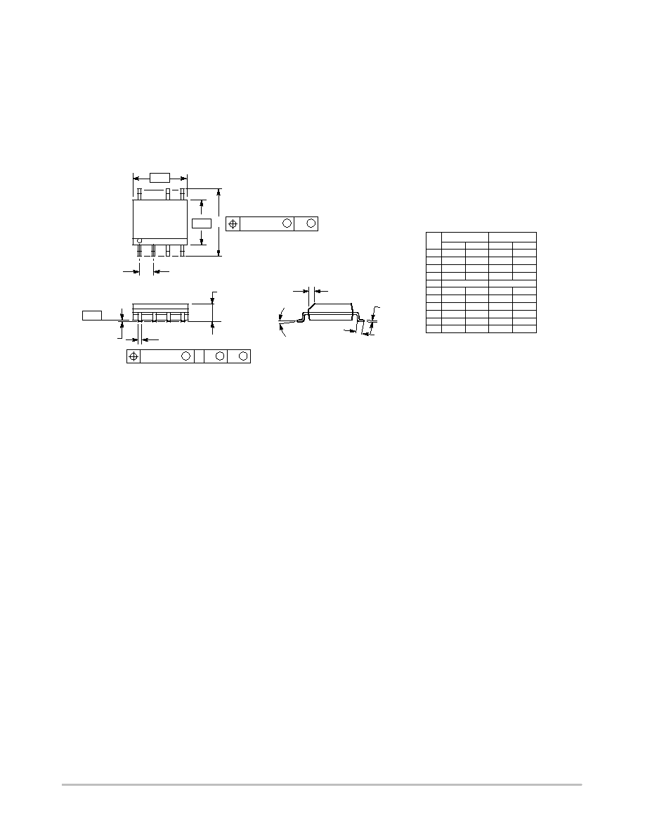
PACKAGE DIMENSIONS
SOIC-7
D SUFFIX
CASE 751U-01
ISSUE C
SEATING
PLANE
1
4
5
8
R
J
X 45
_
K
NOTES:
1. DIMENSIONING AND TOLERANCING PER
ANSI Y14.5M, 1982.
2. CONTROLLING DIMENSION: MILLIMETER.
3. DIMENSION A AND B ARE DATUMS AND T
IS A DATUM SURFACE.
4. DIMENSION A AND B DO NOT INCLUDE
MOLD PROTRUSION.
5. MAXIMUM MOLD PROTRUSION 0.15 (0.006)
PER SIDE.
S
D
H
C
DIM
A
MIN
MAX
MIN
MAX
INCHES
4.80
5.00
0.189
0.197
MILLIMETERS
B
3.80
4.00
0.150
0.157
C
1.35
1.75
0.053
0.069
D
0.33
0.51
0.013
0.020
G
1.27 BSC
0.050 BSC
H
0.10
0.25
0.004
0.010
J
0.19
0.25
0.007
0.010
K
0.40
1.27
0.016
0.050
M
0
8
0
8
N
0.25
0.50
0.010
0.020
S
5.80
6.20
0.228
0.244
-A-
-B-
G
M
B
M
0.25 (0.010)
-T-
B
M
0.25 (0.010)
T
S
A
S
M
7 PL
_
_
_
_
NCP1337
http://onsemi.com
15
PACKAGE DIMENSIONS
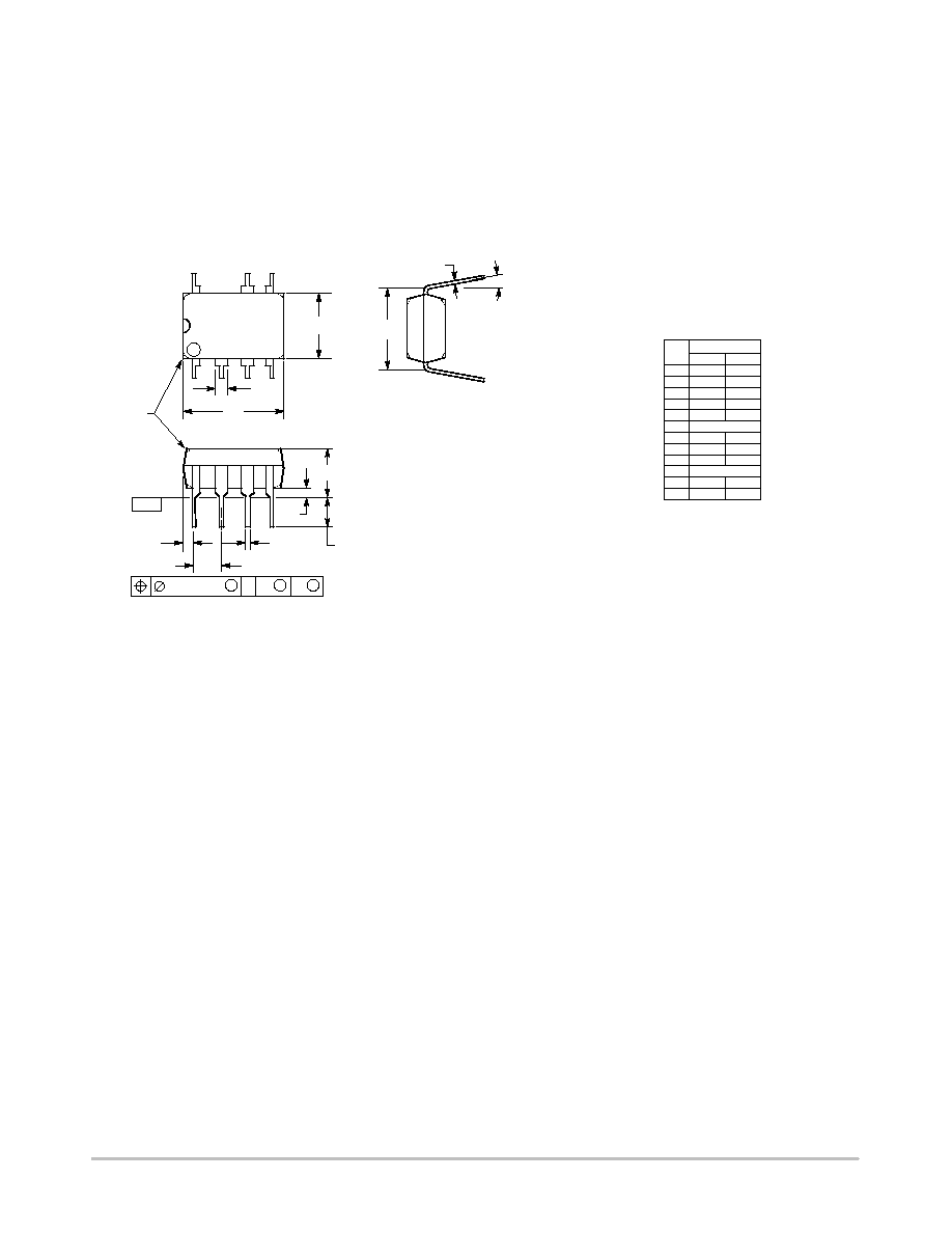
PDIP-7
P SUFFIX
CASE 626B-01
ISSUE A
NOTES:
1. DIMENSIONS AND TOLERANCING PER
ASME Y14.5M, 1994.
2. DIMENSIONS IN MILLIMETERS.
3. DIMENSION L TO CENTER OF LEAD
WHEN FORMED PARALLEL.
4. PACKAGE CONTOUR OPTIONAL (ROUND
OR SQUARE CORNERS).
5. DIMENSIONS A AND B ARE DATUMS.
1
4
5
8
F
NOTE 2
-T-
SEATING
PLANE
H
J
G
D
K
N
C
L
M
M
A
M
0.13 (0.005)
B
M
T
DIM
MIN
MAX
MILLIMETERS
A
9.40
10.16
B
6.10
6.60
C
3.94
4.45
D
0.38
0.51
F
1.02
1.78
G
2.54 BSC
H
0.76
1.27
J
0.20
0.30
K
2.92
3.43
L
7.62 BSC
M
---
10
N
0.76
1.01
∞
A
B

NCP1337
http://onsemi.com
16
ON Semiconductor and are registered trademarks of Semiconductor Components Industries, LLC (SCILLC). SCILLC reserves the right to make changes without further notice
to any products herein. SCILLC makes no warranty, representation or guarantee regarding the suitability of its products for any particular purpose, nor does SCILLC assume any
liability arising out of the application or use of any product or circuit, and specifically disclaims any and all liability, including without limitation special, consequential or incidental
damages. "Typical" parameters which may be provided in SCILLC data sheets and/or specifications can and do vary in different applications and actual performance may vary over
time. All operating parameters, including "Typicals" must be validated for each customer application by customer's technical experts. SCILLC does not convey any license under
its patent rights nor the rights of others. SCILLC products are not designed, intended, or authorized for use as components in systems intended for surgical implant into the body,
or other applications intended to support or sustain life, or for any other application in which the failure of the SCILLC product could create a situation where personal injury or death
may occur. Should Buyer purchase or use SCILLC products for any such unintended or unauthorized application, Buyer shall indemnify and hold SCILLC and its officers, employees,
subsidiaries, affiliates, and distributors harmless against all claims, costs, damages, and expenses, and reasonable attorney fees arising out of, directly or indirectly, any claim of
personal injury or death associated with such unintended or unauthorized use, even if such claim alleges that SCILLC was negligent regarding the design or manufacture of the part.
SCILLC is an Equal Opportunity/Affirmative Action Employer. This literature is subject to all applicable copyright laws and is not for resale in any manner.
PUBLICATION ORDERING INFORMATION
N. American Technical Support: 800-282-9855 Toll Free
USA/Canada
Japan: ON Semiconductor, Japan Customer Focus Center
2-9-1 Kamimeguro, Meguro-ku, Tokyo, Japan 153-0051
Phone: 81-3-5773-3850
NCP1337/D
The product described herein (NCP1337), may be covered by the following U.S. patents: 6,362,067, 5,073,850, 6,385,060, 6,587,357,
6,469,484, 6,940,320, 5,862,045. There may be other patents pending.
LITERATURE FULFILLMENT:
Literature Distribution Center for ON Semiconductor
P.O. Box 61312, Phoenix, Arizona 85082-1312 USA
Phone: 480-829-7710 or 800-344-3860 Toll Free USA/Canada
Fax: 480-829-7709 or 800-344-3867 Toll Free USA/Canada
Email: orderlit@onsemi.com
ON Semiconductor Website: http://onsemi.com
Order Literature: http://www.onsemi.com/litorder
For additional information, please contact your
local Sales Representative.