ˋ
Semiconductor Components Industries, LLC, 2002
June, 2002 Ù Rev. 0
1
Publication Order Number:
NCP1404/D
NCP1404 Series
Product Preview
350 mA PWM/PFM Step-Up
DC-DC Converter with Low
Battery Detector
The NCP1404 series are monolithic PWM/PFM stepÙup DC to DC
converters which can automatically change operation mode from
PWM to PFM at light loads to improve efficiency at light loads. With
only four external components, this series allow a simple means to
implement highly efficient converters for powering up portable
equipment up to 350 mA loading.
Additionally, this series is featured with a Low Battery Detector to
monitor battery voltage. The NCP1404 device series are available in
spaceÙsaving TSOPÙ6 package with five standard regulated output
voltages. Additional voltages that range from 1.8 V to 5.0 V in
100 mV steps can be manufactured.
Features
ñ
Low StartÙUp Voltage of 0.8 V
ñ
PWM Oscillator Frequency of 600 kHz at 20% Accuracy
ñ
High Efficiency 85% at I
OUT
= 200 mA, V
IN
= 2.5 V, V
OUT
= 3.3 V
ñ
Output Current up to 350 mA at V
IN
= 2.5 V, V
OUT
= 3.3 V
ñ
Duty Ratio: 17% to 85% typ. PWM Control
Duty Ratio:
17% typ. PFM Control
ñ
Output Voltage Accuracy
Ý
2.5%
ñ
Low Battery Detection with OpenÙdrain Detector Output
ñ
Separated Power Supply Pin
ñ
Low Profile and Minimum External Parts
ñ
Micro Miniature TSOPÙ6
Typical Applications
ñ
Digital Cameras
ñ
Cellular Telephones
ñ
Personal Digital Assistants (PDA)
ñ
Camcorders
ñ
Electronic Games
ñ
Pagers
ñ
Portable Audio (MP3)
ñ
Handheld Instruments
This document contains information on a product under development. ON Semiconductor
reserves the right to change or discontinue this product without notice.
TSOPÙ6
SN SUFFIX
CASE 318G
1
PIN CONNECTIONS AND
MARKING DIAGRAM
(Top View)
http://onsemi.com
6
Device
Package
Shipping
ORDERING INFORMATION
NCP1404SN19T1
TSOPÙ6
3000/Tape & Reel
XX
d
XX = Specific Device Code
d
= Date Code
LX
LBO
GND
LBI
OUT
V
DD
NCP1404SN27T1
TSOPÙ6
3000/Tape & Reel
NCP1404SN30T1
TSOPÙ6
3000/Tape & Reel
NCP1404SN33T1
TSOPÙ6
3000/Tape & Reel
NCP1404SN50T1
TSOPÙ6
3000/Tape & Reel
6
5
4
1
2
3
See specific marking information in the ordering information
table on page 3 of this data sheet.
NCP1404 Series
http://onsemi.com
2
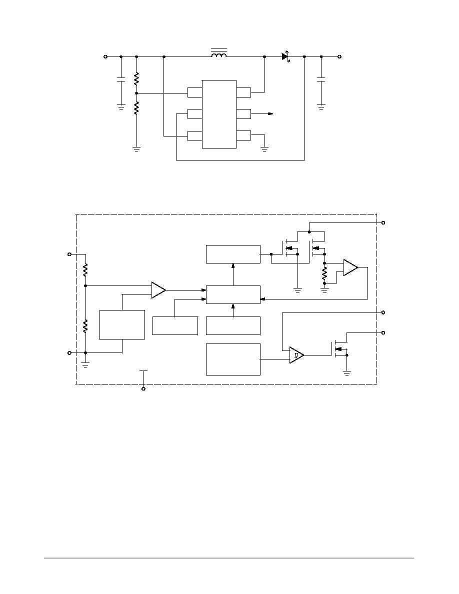
Figure 1. Typical StepÙUp Converter Application
V
IN
0.8 V to 3.0 V
C
1
10
m
F
L
10
m
H
C
2
V
OUT
10
m
F
MBRM110LT1
3.3 V
Figure 2. Representative Block Diagram
DRIVER
PWM/PFM
CONTROLLER
OSCILLATOR
0.4 V
VOLTAGE
REFERENCE
SOFTÙSTART
0.5 V
VOLTAGE
REFERENCE
+
-
ERROR
AMPLIFIER
+
-
-
+
V
DD
V
DD
6
LX
1
LBI
5
LBO
3
OUT
2
GND
4
V
DD
3
OUT
2
LBI
1
GND
4
LBO
5
LX
6
TO
MCU
NCP1404
R
LB2
R
LB1
SD
NCP1404 Series
http://onsemi.com
3
PIN FUNCTION DESCRIPTIONS
Pin
Symbol
Description
1
LBI
Low battery detection input pin
2
OUT
Output voltage monitor pin
3
V
DD
Power supply pin
4
GND
Ground pin
5
LBO
Low battery detection output pin
6
LX
External inductor connection pin to power switch drain
ORDERING INFORMATION
Device
Output Voltage
Frequency
Device Marking
Package
Shipping
NCP1404SN19T1
1.9 V
600 kHz
DB?
NCP1404SN27T1
2.7 V
600 kHz
DB?
NCP1404SN30T1
3.0 V
600 kHz
DB?
TSOPÙ6
3000 Units
per 7 Inch Reel
NCP1404SN33T1
3.3 V
600 kHz
DB?
er 7 Inch Reel
NCP1404SN50T1
5.0 V
600 kHz
DB?
NOTE:
The ordering information lists five standard output voltage device options. Additional device with output voltage ranging from 1.8 V to
5.0 V in 100 mV increments can be manufactured. Contact your ON Semiconductor representative for availability.
MAXIMUM RATINGS
Rating
Symbol
Value
Unit
Power Supply Voltage (Pin 3)
V
DD
Ù0.3 to 6.0
V
Input/Output Pins
Pin 1, Pin 2, Pin 5, Pin 6 Voltage
V
IO
Ù0.3 to 6.0
V
LX Pin Peak Sink Current
I
LX
1000
mA
Thermal Resistance Junction to Air
R
JA
250
_
C/W
Operating Ambient Temperature Range
T
A
Ù40 to + 85
_
C
Operating Junction Temperature Range
T
J
Ù40 to + 125
_
C
Storage Temperature Range
T
stg
Ù55 to +150
_
C
1. This device series contains ESD protection and exceeds the following tests:
Human Body Model (HBM)
"
2.0 kV per JEDEC standard: JESD22ÙA114.
Machine Model (MM)
"
200 V per JEDEC standard: JESD22ÙA115.
2. LatchÙup Current Maximum Rating:
"
150 mA per JEDEC standard: JESD78.
3. Moisture Sensitivity Level (MSL): 1 per IPC/JEDEC standard: JÙSTDÙ020A.
NCP1404 Series
http://onsemi.com
4
ELECTRICAL CHARACTERISTICS
(For all values T
A
= 25
_
C unless otherwise noted.)
Characteristic
Symbol
Min
Typ
Max
Unit
OSCILLATOR
Frequency (V
OUT
= V
SET
æ
0.96) (Note 4)
f
OSC
480
600
720
kHz
Frequency Temperature Coefficient (T
A
= Ù40 to +85
_
C)
D
f
Ù
0.11
Ù
%/
_
C
Maximum PWM Duty Cycle (V
OUT
= V
SET
æ
0.96)
D
MAX
70
78
86
%
PFM Duty Cycle
D
PFM
12
17
22
%
Minimum StartÙup Voltage (I
O
= 0 mA, V
DD
= V
OUT
= V
SET
)
V
start
Ù
0.8
0.95
V
Minimum StartÙup Voltage Temperature Coefficient (T
A
= Ù40 to +85
_
C)
D
V
start
Ù
Ù1.6
Ù
mV/
_
C
SoftÙStart Time (V
OUT
= V
SET
)
t
SS
0.3
2.0
Ù
ms
LX (PIN 6)
Internal Switching NÙChannel FET Drain Voltage
V
LX
Ù
Ù
6.0
V
LX OnÙState Current (V
DD
= V
OUT
= V
SET
æ
0.96, V
LX
= 0.6
V)
Device Suffix:
19T1
27T1
30T1
33T1
50T1
V
LX
350
550
550
550
600
400
600
600
600
650
Ù
Ù
Ù
Ù
Ù
mA
Current Limit
I
LXLIM
700
750
800
mA
OffÙState Leakage Current (V
LX
= 6.0 V, T
A
= Ù40 to +85
_
C)
I
LKG
Ù
0.5
1.0
mA
LBI (PIN 1)
LBI Threshold Voltage Falling
V
LBI
0.396
0.400
0.404
V
LBI Hysteresis
V
HYS
Ù
30
Ù
mV
LBI Input Current
I
LBI
Ù
1.5
8.0
nA
LBO (PIN 5)
LBO Low Output Voltage
V
LBO(low)
Ù
Ù
0.05
V
LBO OffÙState Leakage Current
I
LBOLKG
Ù
1
100
nA
TOTAL DEVICE
Supply Voltage
V
DD
0.8
5.5
V
Output Voltage
Device Suffix:
19T1
27T1
30T1
33T1
50T1
V
OUT
1.853
2.632
2.925
3.218
4.875
1.9
2.7
3.0
3.3
5.0
1.948
2.768
3.075
3.383
5.125
V
Output Voltage Temperature Coefficient (T
A
= Ù40 to +85
_
C)
D
V
OUT
Ù
100
Ù
ppm/
_
C
Operating Current (V
OUT
= V
SET
æ
0.96, V
DD
= V
SET
æ
0.6) (Note 5)
I
DD1
Ù
220
300
m
A
No Switching Operating Current (V
OUT
= V
SET
+
0.5 V)
I
DD2
Ù
40
55
m
A
No Load Operating Current
(V
DD
= V
SET
æ
0.6, I
OUT
= 0 mA ) (Note 7)
I
DD(no load)
Ù
65
80
m
A
Maximum Output Current
(V
DD
= V
OUT
, V
IN
= V
SET
æ
0.8, Voltage Regulation < 3%)
Device Suffix:
19T1
27T1
30T1
33T1
50T1
I
OUT
150
300
300
300
350
200
350
350
350
400
Ù
Ù
Ù
Ù
Ù
mA
4. V
SET
means setting of output voltage.
5. Operating current is the current consumption of the device in PWM mode.
6. No switching operating current is the current consumption of the device when there is no switching.
7. No load operating current is the current consumption of the device in PFM mode at no load.
NCP1404 Series
http://onsemi.com
5
Other Application Circuit
Figure 3. StepÙdown Application
V
IN
5.0 V
33
m
F
L
V
OUT
33
m
F
MBR0520LT1
3.3 V
V
DD
3
OUT
2
LBI
1
GND
4
LBO
5
LX
6
To MCU
I/O Pin
NCP1404
R
LB2
R
LB1
GND
+
+
820
MGSF1P02LT1
NCP1404 Series
http://onsemi.com
6
PACKAGE DIMENSIONS
TSOPÙ6
CASE 318GÙ02
ISSUE H
2
3
4
5
6
A
L
1
S
G
D
B
H
C
0.05 (0.002)
DIM
MIN
MAX
MIN
MAX
INCHES
MILLIMETERS
A
0.1142 0.1220
2.90
3.10
B
0.0512 0.0669
1.30
1.70
C
0.0354 0.0433
0.90
1.10
D
0.0098 0.0197
0.25
0.50
G
0.0335 0.0413
0.85
1.05
H
0.0005 0.0040
0.013
0.100
J
0.0040 0.0102
0.10
0.26
K
0.0079 0.0236
0.20
0.60
L
0.0493 0.0610
1.25
1.55
M
0
10
0
10
S
0.0985 0.1181
2.50
3.00
_
_
_
_
NOTES:
1. DIMENSIONING AND TOLERANCING PER ANSI
Y14.5M, 1982.
2. CONTROLLING DIMENSION: MILLIMETER.
3. MAXIMUM LEAD THICKNESS INCLUDES LEAD
FINISH THICKNESS. MINIMUM LEAD THICKNESS
IS THE MINIMUM THICKNESS OF BASE
MATERIAL.
M
J
K

NCP1404 Series
http://onsemi.com
7
Notes

NCP1404 Series
http://onsemi.com
8
ON Semiconductor and are registered trademarks of Semiconductor Components Industries, LLC (SCILLC). SCILLC reserves the right to make
changes without further notice to any products herein. SCILLC makes no warranty, representation or guarantee regarding the suitability of its products for any
particular purpose, nor does SCILLC assume any liability arising out of the application or use of any product or circuit, and specifically disclaims any and all
liability, including without limitation special, consequential or incidental damages. "Typical" parameters which may be provided in SCILLC data sheets and/or
specifications can and do vary in different applications and actual performance may vary over time. All operating parameters, including "Typicals" must be
validated for each customer application by customer's technical experts. SCILLC does not convey any license under its patent rights nor the rights of others.
SCILLC products are not designed, intended, or authorized for use as components in systems intended for surgical implant into the body, or other applications
intended to support or sustain life, or for any other application in which the failure of the SCILLC product could create a situation where personal injury or death
may occur. Should Buyer purchase or use SCILLC products for any such unintended or unauthorized application, Buyer shall indem nify and hold SCILLC and
its officers, employees, subsidiaries, affiliates, and distributors harmless against all claims, costs, damages, and expenses, and reasonable attorney fees
arising out of, directly or indirectly, any claim of personal injury or death associated with such unintended or unauthorized use, even if such claim alleges that
SCILLC was negligent regarding the design or manufacture of the part. SCILLC is an Equal Opportunity/Affirmative Action Employer.
PUBLICATION ORDERING INFORMATION
JAPAN: ON Semiconductor, Japan Customer Focus Center
4Ù32Ù1 NishiÙGotanda, ShinagawaÙku, Tokyo, Japan 141Ù0031
Phone: 81Ù3Ù5740Ù2700
Email: r14525@onsemi.com
ON Semiconductor Website: http://onsemi.com
For additional information, please contact your local
Sales Representative.
NCP1404/D
Literature Fulfillment:
Literature Distribution Center for ON Semiconductor
P.O. Box 5163, Denver, Colorado 80217 USA
Phone: 303Ù675Ù2175 or 800Ù344Ù3860 Toll Free USA/Canada
Fax: 303Ù675Ù2176 or 800Ù344Ù3867 Toll Free USA/Canada
Email: ONlit@hibbertco.com
N. American Technical Support: 800Ù282Ù9855 Toll Free USA/Canada