 | –≠–ª–µ–∫—Ç—Ä–æ–Ω–Ω—ã–π –∫–æ–º–ø–æ–Ω–µ–Ω—Ç: NCP1417 | –°–∫–∞—á–∞—Ç—å:  PDF PDF  ZIP ZIP |

©
Semiconductor Components Industries, LLC, 2002
April, 2002 ≠ Rev. 1
1
Publication Order Number:
NCP1417/D
NCP1417
200 mA DC-DC Step-up
Converter with Dual Low
Battery Protection
NCP1417 is a monolithic micropower high frequency Boost
(step≠up) voltage switching converter IC specially designed for
battery operated hand≠held electronic products up to 200 mA loading.
It integrates Synchronous Rectifier for improving efficiency as well as
eliminating the external Schottky Diode. High switching frequency
(up to 600 kHz) allows use of a low profile inductor and output
capacitor. Dual Low≠Battery Detectors and Cycle≠by≠Cycle Current
Limit provide value≠added features for various battery≠operated
applications. With all these functions ON, the quiescent supply current
is only 9.0
mA typical. This device is available in a space saving
compact Micro8
t package.
Features
∑
High Efficiency, Up to 92%, Typical
∑
Very Low Device Quiescent Supply Current of 9.0
mA Typical
∑
Built≠in Synchronous Rectifier (P≠FET) Eliminates One External
Schottky Diode
∑
High Switching Frequency (Up to 600 kHz) Allows Small Size
Inductor and Capacitor
∑
High Accuracy Reference Output, 1.19 V
±
0.6% @ 25
_C, Can
Supply More Than 2.5 mA when V
OUT
3.3 V
∑
1.0 V Startup at No Load Guaranteed
∑
Output Voltage from 1.5 V to 5.5 V Adjustable
∑
Output Current Up to 200 mA @ V
in
= 2.5 V, V
out
= 3.3 V
∑
Multi≠Function LBI/Shutdown Control Pin
∑
Dual Open Drain Low≠Battery Detector Outputs
∑
1.0 A Cycle by Cycle Current Limit
∑
Low Profile and Minimum External Parts
∑
Compact Micro8 Package
Applications
∑
Personal Digital Assistants (PDA)
∑
Handheld Digital Audio Product
∑
Camcorders and Digital Still Camera
∑
Handheld Instrument
∑
Conversion from One or Two NiMH or NiCd or One Lithium≠ion
Cells to 3.3 V/5.0 V
Device
Package
Shipping
ORDERING INFORMATION
NCP1417DMR2
Micro8
4000 Tape & Reel
Micro8
DM SUFFIX
CASE 846A
1
8
MARKING
DIAGRAM
1417
AYW
1
8
PIN CONNECTIONS
1417 = Device Marking
A
= Assembly Location
Y
= Year
W
= Work Week
8
7
6
5
1
2
3
4
FB
LBI/SHDN
LBO1
REF
OUT
LX
GND
LBO2
(Top View)
http://onsemi.com
NCP1417
http://onsemi.com
2
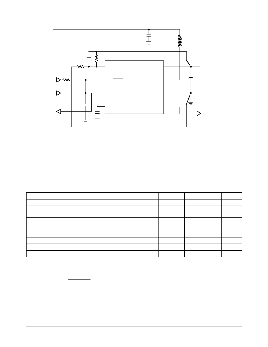
Figure 1. Typical Operating Circuit
NCP1417
FB
LBI/SHDN
LBO1
REF
VOUT
LX
GND
LBO2
355 K
150 pF
200 K
56 nF
150 nF
Low Battery
Sense Input
Shutdown
Input
Low Battery
Open Drain
Output 1
Input
1.0 V to
V
OUT
10
m
F
22
m
H
+
V
OUT
33
m
F
Output 1.5 V to 5.5 V
I
OUT
typical up to
200 mA at 3.3 V Output
and 2.5 V Input
Low Battery
Open Drain
Output 2
MAXIMUM RATINGS
Rating
Symbol
Value
Unit
Power Supply (Pin 8)
V
OUT
≠0.3 to 6.0
V
Input/Output Pins
Pin 1≠5, Pin 7
V
IO
≠0.3 to 6.0
V
Thermal Characteristics
Micro8 Plastic Package
Maximum Power Dissipation @ T
A
= 25
∞
C
Thermal Resistance Junction to Air
P
D
R
q
JA
520
240
mW
_
C/W
Operating Junction Temperature Range
T
J
≠40 to +150
_
C
Operating Ambient Temperature Range
T
A
≠40 to +85
_
C
Storage Temperature Range
T
stg
≠55 to +150
_
C
1. This device contains ESD protection and exceeds the following tests:
Human Body Model (HBM)
"
2.0 kV per JEDEC standard: JESD22≠A114
.
Machine Model (MM)
"
200 V per JEDEC standard: JESD22≠A115.
2. The maximum package power dissipation limit must not be exceeded.
PD
+
TJ(max)
*
TA
R
q
JA
3. Latch≠up Current Maximum Rating:
"
150 mA per JEDEC standard: JESD78.
4. Moisture Sensitivity Level: MSL 1 per IPC/JEDEC standard: J≠STD≠020A.
NCP1417
http://onsemi.com
3
ELECTRICAL CHARACTERISTICS
(V
OUT
= 3.3 V, T
A
= 25
∞
C for typical value, ≠40
∞
C
T
A
85
_
C for min/max values unless
otherwise noted.)
Characteristics
Symbol
Min
Typ
Max
Unit
Operating Voltage
V
IN
1.0
≠
5.5
V
Output Voltage Range (Adjusted by External Feedback)
V
OUT
V
IN
≠
5.5
V
Reference Voltage (C
REF
= 150 nF, Under No Loading,
T
A
= 25
_
C)
V
REF_NL
1.183
1.190
1.197
V
Reference Voltage (C
REF
= 150 nF, Under No Loading,
≠40
_
C
T
A
85
_
C)
V
REF_NL_A
1.178
≠
1.202
V
Reference Voltage Temperature Coefficient
TC
VREF
≠
0.03
≠
mV/
_
C
Reference Voltage Load Current
(V
OUT
= 3.3 V, V
REF
= V
REF_NL
"
1.5%, C
REF
= 1.0
m
F) (Note 5
)
I
REF
2.5
≠
≠
mA
Reference Voltage Load Regulation
(V
OUT
= 3.3 V, I
LOAD
= 0 to 100
m
A, C
REF
= 1.0
m
F)
V
REF_LOAD
≠
0.015
1.0
mV
Reference Voltage Line Regulation
V
REF_LINE
≠
0.03
1.0
mV/V
FB, LBI Input Threshold
V
FB,
V
LBI
1.172
1.190
1.200
V
Internal NFET ON≠Resistance (I
LX
= 100 mA)
R
DS(ON)_N
≠
0.65
≠
W
Internal PFET ON≠Resistance (I
LX
= 100 mA)
R
DS(ON)_P
≠
1.3
≠
W
LX Switch Current Limit (NFET)
I
LIM
≠
1.0
≠
A
Operating Current into OUT
(V
FB
= 1.4 V, i.e. No Switching, V
OUT
= 3.3 V)
I
Q
≠
9.0
14
m
A
Shutdown Current into OUT (SHDN = GND)
I
SD
≠
0.05
1.0
m
A
LX Switch MAX. ON≠Time (V
FB
= 1.0 V, V
OUT
= 3.3 V)
t
ON
0.8
1.4
2.0
m
S
LX Switch MIN. OFF≠Time (V
FB
= 1.0 V, V
OUT
= 3.3 V)
t
OFF
0.22
0.25
0.46
m
S
FB Input Current
I
FB
≠
1.5
20
nA
LBI/SHDN Input Current
I
LBI,
I
SHDN
≠
1.5
8.0
nA
LBO1/LBO2 Low Output Voltage (V
LBI
= 0, I
SINK
= 1.0 mA)
V
LBO_L1
V
LBO_L2
≠
≠
≠
≠
0.08
0.08
V
LBI/SHDN Input Threshold for LBO1
V
LBI1
1.172
1.190
1.200
V
LBI/SHDN Input Threshold for LBO2
V
LBI2
0.904
0.944
0.965
V
LBI/SHDN Input Threshold, Low
V
SHDN_L
≠
≠
0.3
V
LBI/SHDN Input Threshold, High
V
SHDN_H
0.6
≠
≠
V
5. Loading capability decreases with V
OUT
.
PIN FUNCTION DESCRIPTION
Pin No.
Pin Name
Pin Description
1
FB
Output Voltage Feedback Input.
2
LBI/SHDN
Low≠Battery Detector Input and Shutdown Control input multi≠function pin.
3
LBO1
Open≠Drain Low≠Battery Detector Output. Output is LOW when VLBI is < 1.172 V. LBO1 is high
impedance during shutdown.
4
REF
1.190 V Reference Voltage Output, bypassing with 150 nF capacitor if this pin is not loaded,
bypassing with 1
µ
F if this pin is loaded up to 2.5 mA @ V
OUT
= 3.3 V.
5
LBO2
Open≠Drain Low≠Battery Detector Output. Output is LOW when VLBI is < 0.904 V. LBO2 is high
impedance during shutdown.
6
GND
Ground
7
LX
N≠Channel and P≠Channel Power MOSFET Drain Connection.
8
OUT
Power Output. OUT provides bootstrap power to the IC.
NCP1417
http://onsemi.com
4
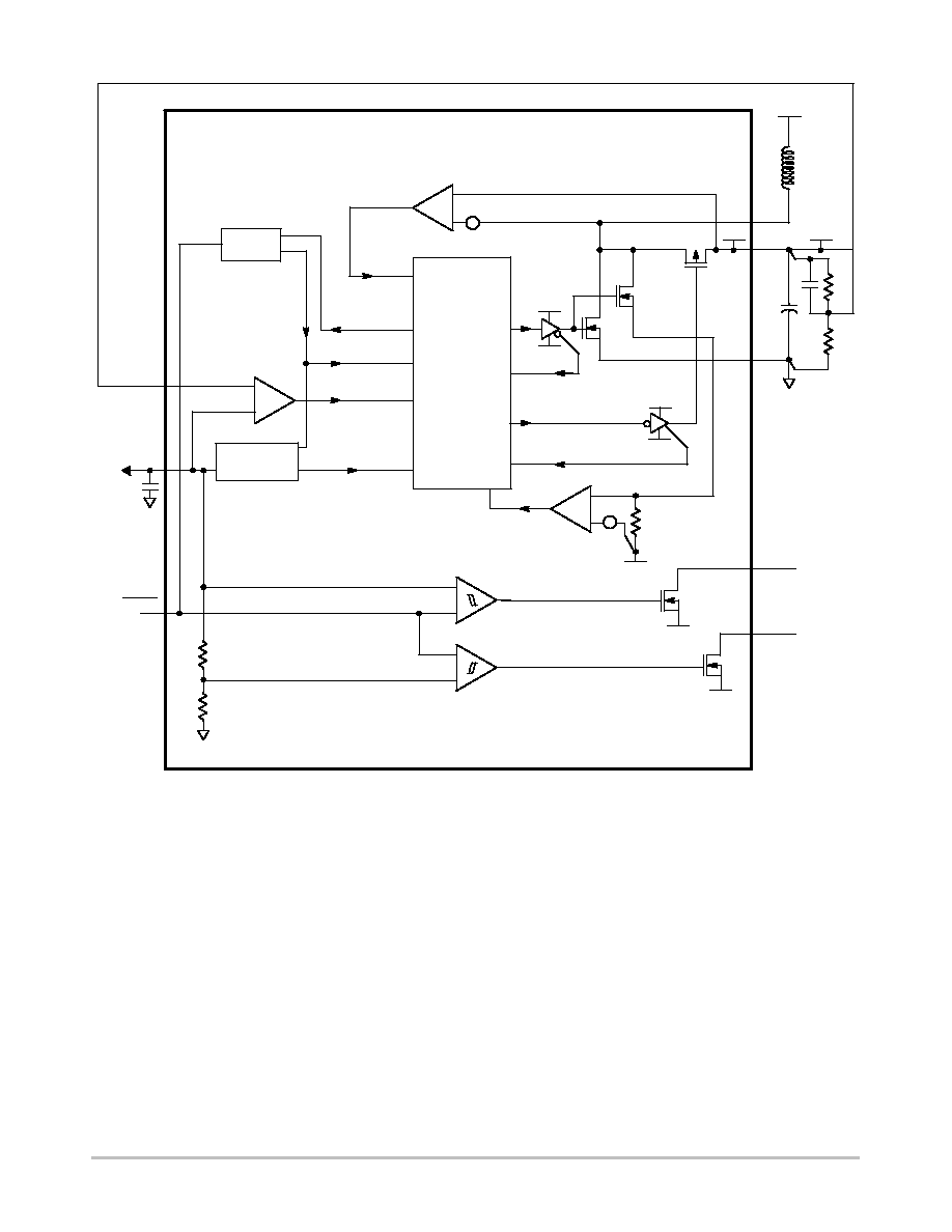
Figure 2. Simplified Functional Diagram
CONTROL
LOGIC
_MAINSW2ON
_SYNSW2ON
_ZCUR
_PWGONCE
_CEN
_PFM
ZLC
+
≠
CHIP
ENABLE
PFM
+
≠
VOLTAGE
REFERENCE
_VREFOK
REF
LBI/SHDN
FB
VDD
GND
M1
SenseFET
M2
VDD
LX
OUT
GND
VOUT
VBAT
_MAINSWOFD
ILIM
+
≠
_SYNSWOFD
GND
+
VDD
GND
+
≠
+
≠
VREF
0.8 x VREF
30 mV
CP2
30 mV
CP1
GND
LBO1
GND
LBO2
+
20 mV
_ILIM
1
4
2
7
8
6
5
3
NCP1417
http://onsemi.com
5
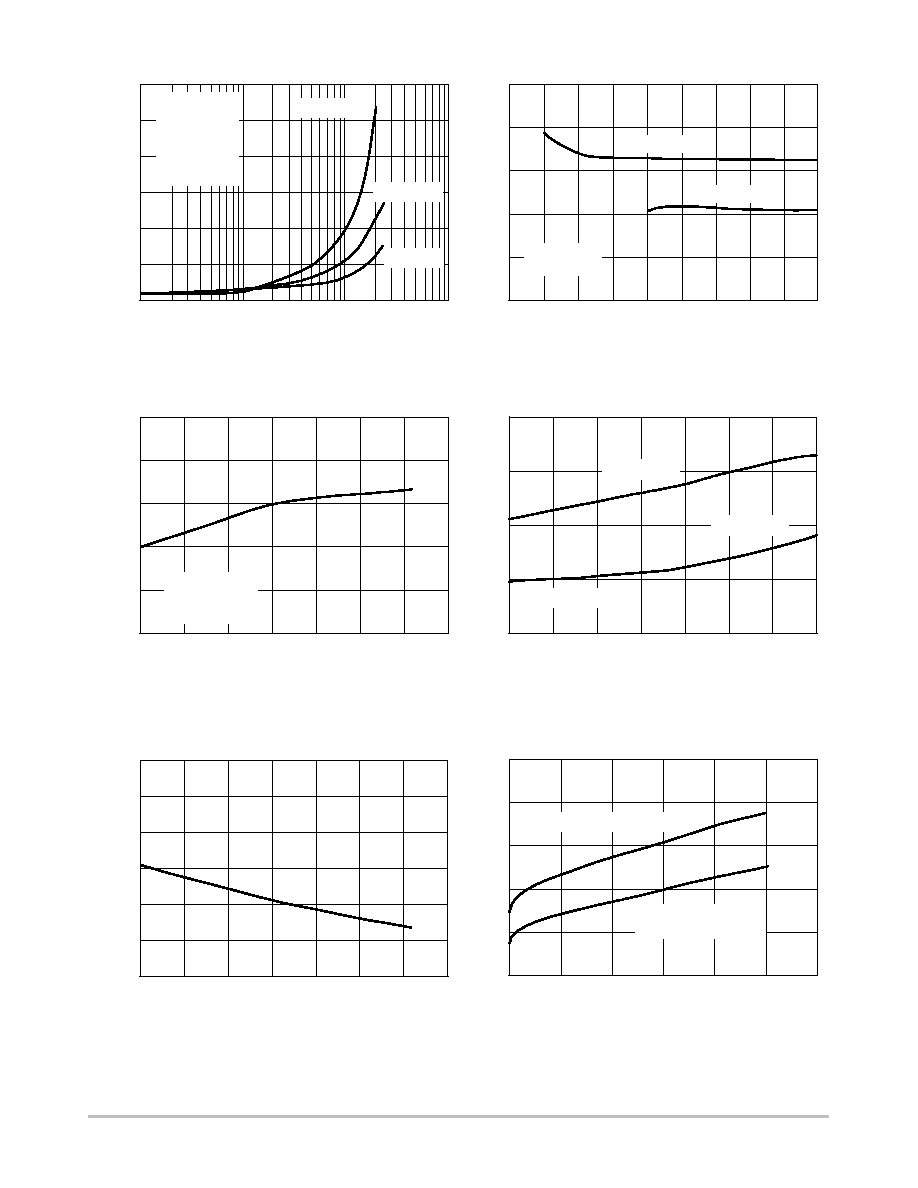
I
REF
= 0 mA
REFERENCE VOL
T
AGE, V
REF
/V
1.190
1.195
1.200
1.205
1.210
1.215
1.220
OUTPUT CURRENT, I
LOAD
/mA
Figure 3. Reference Voltage versus
Output Current
1
10
100
1000
1
2
3
4
5
5.5
4.5
1.5
2.5
3.5
1.180
1.183
1.186
1.189
1.192
1.195
REFERENCE VOL
T
AGE, V
REF
/V
INPUT VOLTAGE at OUT PIN, V
OUT
/V
Figure 4. Reference Voltage versus
Input Voltage at OUT Pin
1.184
1.186
1.188
1.19
1.192
1.194
≠40
≠20
0
20
40
60
80
100
REFERENCE VOL
T
AGE, V
REF
/V
AMBIENT TEMPERATURE, T
A
/
_
C
Figure 5. Reference Voltage versus
Temperature
0
0.5
1
2
≠40
≠20
0
20
40
60
80
100
SWITCH ON RESIST
ANCE, R
DS
(ON)
/
AMBIENT TEMPERATURE, T
A
/
_
C
Figure 6. Switch ON Resistance
versus Temperature
1.5
1.2
1.4
1.5
1.6
1.7
1.8
≠40
≠20
0
20
40
60
80
100
L
x
SWITCH MAX. ON TIME, t
ON
/
µ
S
AMBIENT TEMPERATURE, T
A
/
_
C
Figure 7. L
x
Switch Max. ON Time
versus Temperature
1.3
0.6
0.9
1.2
2.1
0
20
40
60
80
120
MIN.
ST
AR
TUP BA
TTER
Y VOL
T
AGE, V
BA
TT
/V
OUTPUT LOADING CURRENT, I
LOAD
/mA
Figure 8. Min. Startup Battery Voltage
versus Loading Current
1.8
I
REF
= 2.5 mA
C
REF
= 1
µ
F
T
A
= 25
_
C
V
OUT
= 3.3 V
C
REF
= 150 nF
I
REF
= 0 mA
V
OUT
= 3.3 V
P≠FET (M2)
N≠FET (M1)
1.5
100
Without Schottky Diode
With Schottky Diode
(MBR0502)
V
OUT
= 3.3 V
L = 22
µ
H
C
in
= 10
µ
F
C
out
= 33
µ
F
C
REF
= 1
µ
F
T
A
= 25
_
C
V
IN
= 1.8 V
V
IN
= 2.2 V
V
IN
= 3 V

NCP1417
http://onsemi.com
6
EFFICIENCY/%
OUTPUT LOADING CURRENT, I
LOAD
/mA
1
10
100
1000
50
60
70
80
90
100
EFFICIENCY/%
50
60
70
80
90
100
OUTPUT LOADING CURRENT, I
LOAD
/mA
1
10
100
1000
EFFICIENCY/%
OUTPUT LOADING CURRENT, I
LOAD
/mA
1
10
100
1000
50
60
70
80
90
100
EFFICIENCY/%
50
60
70
80
90
100
OUTPUT LOADING CURRENT, I
LOAD
/mA
1
10
100
1000
EFFICIENCY/%
L = 27
µ
H
EFFICIENCY/%
50
60
70
80
90
100
OUTPUT LOADING CURRENT, I
LOAD
/mA
Figure 9. Efficiency versus Load Current
1
10
100
1000
OUTPUT LOADING CURRENT, I
LOAD
/mA
Figure 10. Efficiency versus Load Current
Figure 11. Efficiency versus Load Current
Figure 12. Efficiency versus Load Current
Figure 13. Efficiency versus Load Current
Figure 14. Efficiency versus Load Current
V
IN
= 2.2 V
V
OUT
= 5 V
C
IN
= 10
µ
F
C
OUT
= 33
µ
F
1
10
100
1000
50
60
70
80
90
100
L = 22
µ
H
L = 15
µ
H
L = 10
µ
H
V
IN
= 1.8 V
V
OUT
= 3.3 V
C
IN
= 10
µ
F
C
OUT
= 33
µ
F
L = 22
µ
H
V
IN
= 2.2 V
V
OUT
= 3.3 V
C
IN
= 10
µ
F
C
OUT
= 33
µ
F
L = 22
µ
H
L = 15
µ
H
L = 10
µ
H
V
IN
= 3 V
V
OUT
= 5 V
C
IN
= 10
µ
F
C
OUT
= 33
µ
F
L = 22
µ
H
L = 27
µ
H
V
IN
= 3 V
V
OUT
= 3.3 V
C
IN
= 10
µ
F
C
OUT
= 33
µ
F
L = 22
µ
H
L = 15
µ
H
L = 10
µ
H
V
IN
= 4.5 V
V
OUT
= 5 V
C
IN
= 10
µ
F
C
OUT
= 33
µ
F
L = 22
µ
H
L = 27
µ
H

NCP1417
http://onsemi.com
7
RIPPLE VOL
T
AGE, V
RIPPLE
/mV
p≠p
0
20
40
60
80
100
BATTERY INPUT VOLTAGE, V
BATT
/V
1
1.5
2.5
3
V
OUT
= 3.3 V
C
IN
= 10
µ
F
C
OUT
= 33
µ
F
L = 15
m
H
100 mA
2
150 mA
OUTPUT VOL
T
AGE CHANGE/%
≠3
≠2
≠1
0
1
3
OUTPUT LOADING CURRENT, I
LOAD
/mA
1
10
100
1000
L = 15
m
H
V
OUT
= 3.3 V
C
IN
= 10
µ
F
C
OUT
= 33
µ
F
2
3 V
1.8 V
2.2 V
NO LOAD OPERA
TING CURRENT
, I
BA
TT
/
µ
A
0
4
8
12
16
20
INPUT VOLTAGE AT OUT PIN, V
OUT
/V
0
1
2
6
RIPPLE VOL
T
AGE, V
RIPPLE
/mV
p≠p
0
20
40
60
80
100
BATTERY INPUT VOLTAGE, V
BATT
/V
1
1.5
2.5
3
OUTPUT VOL
T
AGE CHANGE/%
≠3
≠2
≠1
0
1
3
OUTPUT LOADING CURRENT, I
LOAD
/mA
Figure 15. Output Voltage Change
versus Load Current
1
10
100
1000
Figure 16. Output Voltage Change versus
Load Current
Figure 17. Battery Input Voltage versus
Output Ripple Voltage
Figure 18. Battery Input Voltage versus
Output Ripple Voltage
Figure 19. No Load Operating Current
versus Input Voltage at OUT Pin
Figure 20. Startup Transient Response
L = 22
m
H
V
OUT
= 3.3 V
C
IN
= 10
µ
F
C
OUT
= 33
µ
F
V
OUT
= 3.3 V
C
IN
= 10
µ
F
C
OUT
= 33
µ
F
L = 22
m
H
100 mA
2
3 V
1.8 V
2.2 V
2
150 mA
3
4
5
(V
IN
= 2.2 V, V
OUT
= 3.3 V, I
LOAD
= 100 mA; L = 22
µ
H,
C
OUT
= 33
µ
F)
Upper Trace: Output Voltage Waveform, 1.0 V/Division
Lower Trace: Shutdown Pin Waveform, 1.0 V/Division

NCP1417
http://onsemi.com
8
Figure 21. Continuous Conduction
Mode Switching Waveform
Figure 22. Discontinuous Conduction
Mode Switching Waveform
(V
IN
= 2.2 V, V
OUT
= 3.3 V, I
LOAD
= 100 mA; L = 22
µ
H,
C
OUT
= 33
µ
F)
Upper Trace: Voltage at L
X
pin, 2.0 V/Division
Middle Trace: Output Voltage Ripple, 50 mV/Division
Lower Trace: Inductor Current, I
L
, 100 mA/Division
Figure 23. Line Transient Response for V
OUT
= 3.3 V
(V
IN
= 2.2 V, V
OUT
= 3.3 V, I
LOAD
= 30 mA; L = 22
µ
H,
C
OUT
= 33
µ
F)
Upper Trace: Voltage at L
X
pin, 2.0 V/Division
Middle Trace: Output Voltage Ripple, 50 mV/Division
Lower Trace: Inductor Current, I
L
, 100 mA/Division
Figure 24. Load Transient Response for V
IN
= 1.8 V
(V
IN
= 1.8 V, V
OUT
= 3.0 V, L = 22
µ
H, C
OUT
= 33
µ
F)
Upper Trace: Output Voltage Ripple, 100 mV/Division
Lower Trace: Battery Voltage, V
IN
, 1.0 V/Division
(V
OUT
= 3.3 V, I
LOAD
= 10 mA to 100 mA; L = 22
µ
H,
C
OUT
= 33
µ
F)
Upper Trace: Output Voltage Ripple, 100 mV/Division
Lower Trace: Load Current, I
LOAD
, 50 mA/Division
Figure 25. Load Transient Response for V
IN
= 2.4 V
(V
OUT
= 3.3 V, I
LOAD
= 10 mA to 100 mA; L = 22
µ
H,
C
OUT
= 33
µ
F)
Upper Trace: Output Voltage Ripple, 100 mV/Division
Lower Trace: Load Current, I
LOAD
, 50 mA/Division
Figure 26. Load Transient Response for V
IN
= 3.3 V
(V
OUT
= 3.3 V, I
LOAD
= 10 mA to 100 mA; L = 22
µ
H,
C
OUT
= 33
µ
F)
Upper Trace: Output Voltage Ripple, 100 mV/Division
Lower Trace: Load Current, I
LOAD
, 50 mA/Division

NCP1417
http://onsemi.com
9
DETAILED OPERATION DESCRIPTIONS
NCP1417 is a monolithic micropower high frequency
step≠up voltage switching converter IC specially designed
for battery operated hand≠held electronic products up to
200 mA loading. It integrates Synchronous Rectifier for
improving efficiency as well as eliminating the external
Schottky Diode. High switching frequency (up to 600 kHz)
allows low profile inductor and output capacitor being used.
Dual Low≠Battery Detectors, Logic≠Controlled Shutdown
and Cycle≠by≠Cycle Current Limit provide value≠added
features for various battery≠operated application. With all
these functions ON, the quiescent supply current is only
9
µ
A typical. This device is available in compact Micro8
package.
PFM Regulation Scheme
From the simplified Functional Diagram (Figure 2), the
output voltage is divided down and fed back to pin 1 (FB).
This voltage goes to the non≠inverting input of the PFM
comparator whereas the comparator's inverting input is
connected to REF. A switching cycle is initiated by the
falling edge of the comparator, at the moment, the main
switch (M1) is turned ON. After the maximum ON≠time
(typical 1.4
mS) elapses or the current limit is reached, M1
is turned OFF, and the synchronous switch (M2) is turned
ON. The M1 OFF time is not less than the minimum
OFF≠time (typical 0.25
mS), this is to ensure energy transfer
from the inductor to the output capacitor. If the regulator is
operating at continuous conduction mode (CCM), M2 is
turned OFF just before M1 is supposed to be ON again. If the
regulator is operating at discontinuous conduction mode
(DCM), which means the coil current will decrease to zero
before the next cycle, M1 is turned OFF as the coil current
is almost reaching zero. The comparator (ZLC) with fixed
offset is dedicated to sense the voltage drop across M2 as it
is conducting, when the voltage drop is below the offset, the
ZLC comparator output goes HIGH, and M2 is turned OFF.
Negative feedback of closed loop operation regulates
voltage at pin 1 (FB) equal to the internal voltage reference
(1.190 V).
Synchronous Rectification
Synchronous Rectifier is used to replace Schottky Diode
to eliminate the conduction loss contributed by forward
voltage drop of the latter. Synchronous Rectifier is normally
realized by powerFET with gate control circuitry which,
however, involved relative complicated timing concerns.
As main switch M1 is being turned OFF, if the
synchronous switch M2 is just turned ON with M1 not being
completed turned OFF, current will be shunt from the output
bulk capacitor through M2 and M1 to ground. This power
loss lowers overall efficiency. So a certain amount of dead
time is introduced to make sure M1 is completely OFF
before M2 is being turned ON.
When the main regulator is operating in CCM, as M2 is
being turned OFF, and M1 is just turned ON with M2 not
being completely turned OFF, the above mentioned
situation
will occur. So dead time is introduced to make sure
M2 is completely turned OFF before M1 is being turned ON.
When the regulator is operating in DCM, as coil current
is dropped to zero, M2 is supposed to be OFF. Fail to do so,
reverse current will flow from the output bulk capacitor
through M2 and then the inductor to the battery input. It
causes damage to the battery. So the ZLC comparator comes
with fixed offset voltage to switch M2 OFF before any
reverse current builds up. However, if M2 is switch OFF too
early, large residue coil current flows through the body diode
of M2 and increases conduction loss. Therefore,
determination on the offset voltage is essential for optimum
performance.
With the implementation of synchronous rectification,
efficiency can be as high as 92%. For single cell input
voltage, use an external schottky diode such as MBR0520
connected from pin 7 to pin 8 to ensure quick start≠up.
Cycle≠by≠Cycle Current Limit
From Figure 2, SenseFET is applied to sample the coil
current as M1 is ON. With that sample current flowing
through a sense resistor, sense≠voltage is developed.
Threshold detector (ILIM) detects whether the
sense≠voltage is higher than preset level. If it happens,
detector output signifies the CONTROL LOGIC to switch
OFF M1, and M1 can only be switched ON as next cycle
starts after the minimum OFF≠time (typical 0.25
mS). With
properly sizing of SenseFET and sense resistor, the peak coil
current limit is set at 1.0 A typically.
Voltage Reference
The voltage at REF is set typically at +1.190 V. It can
deliver up to 2.5 mA with load regulation
±
1.5%, at VOUT
equal to 3.3 V. If VOUT is increased, the REF load
capability can also be increased. A bypass capacitor of
0.15
mF is required for proper operation when REF is not
loaded. If REF is loaded, 1.0
mF capacitor at REF is needed.
Shutdown
The IC is shutdown when the voltage at pin 2
(LBI/SHDN) is pulled lower than 0.3 V via an open drain
transistor. During shutdown, M1 and M2 are both switched
OFF, however, the body diode of M2 allows current flow
from battery to the output, the IC internal circuit will
consume less than 0.05
mA current typically. If the pin 2 pull
low is released, the IC will be enabled. The internal circuit
will only consume 9.0
mA current typically from the OUT
pin.
Dual Low≠Battery Detection
Two comparators with 30 mV hysteresis are applied to
perform the dual low≠battery detection function. When pin
2 (LBI) is at a voltage, which can be defined by a resistor
divider from the battery voltage, lower than the internal
reference voltage, 1.190 V, the first comparator, CP1 output
will cause a 50
W low side switch to be turned ON. It will
pull down the voltage at pin 3 (LBO1) which has a hundreds
kilo≠Ohm of pull≠high resistance. If the pin 2 voltage is
NCP1417
http://onsemi.com
10
higher than 1.190 V + 30 mV, the comparator output will
cause the 50
W low side switch to be turned OFF, pin 3 will
become high impedance, and its voltage will be pulled high.
The second low≠battery detector functions in the same
manner, the second comparator, CP2 with a lower triggering
reference point derived from the internal reference is used
instead, typical 0.944 V. This configuration provides two
levels of low battery warning to the target system.
APPLICATIONS INFORMATION
Output Voltage Setting
The output voltage of the converter is determined by the
external feedback network comprised of R
FB1
and R
FB2
and
the relationship is given by:
VOUT
+
1.190 V
1
)
RFB1
RFB2
where R
FB1
and R
FB2
are the upper and lower feedback
resistors respectively.
Low Battery Detect Level Setting
The Low Battery Detect Voltages of the converter are
determined by the external divider network comprised of
R
LB1
and R
LB2
and the relationship is given by:
VLB1
+
1.190 V
1
)
RLB1
RLB2
where R
LB1
and R
LB2
are the upper and lower divider
resistors respectively. By setting the V
LB1
, the second low
battery detection point, V
LB2
will be fixed automatically.
Inductor Selection
The NCP1417 is tested to produce optimum performance
with a 22
mH inductor at V
IN
= 3.0 V, V
OUT
= 3.3 V
supplying output current up to 200 mA. For other
input/output requirements, inductance in the range 10
mH to
47
mH can be used according to end application
specifications. Selecting an inductor is a compromise
between output current capability and tolerable output
voltage ripple. Of course, the first thing we need to obey is
to keep the peak inductor current below its saturation limit
at maximum current and the I
LIM
of the device. In NCP1417,
I
LIM
is set at 1.0 A. As a rule of thumb, low inductance
values supply higher output current, but also increase the
ripple at output and reducing efficiency, on the other hand,
high inductance values can improve output ripple and
efficiency, however it also limit the output current capability
at the same time. One other parameter of the inductor is its
DC resistance, this resistance can introduce unwanted
power loss and hence reduce overall efficiency, the basic
rule is selecting an inductor with lowest DC resistance
within the board space limitation of the end application.
Capacitors Selection
In all switching mode boost converter applications,
both the input and output terminals sees impulsive
voltage/current waveforms. The currents flowing into and
out of the capacitors multiplying with the Equivalent Series
Resistance (ESR) of the capacitor producing ripple voltage
at the terminals. During the syn≠rect switch off cycle, the
charges stored in the output capacitor is used to sustain the
output load current. Load current at this period and the ESR
combined and reflected as ripple at the output terminal. For
all cases, the lower the capacitor ESR, the lower the ripple
voltage at output. As a general guide line, low ESR
capacitors should be used. Ceramic capacitors have the
lowest ESR, but low ESR tantalum capacitors can also be
used as a cost effective substitute.
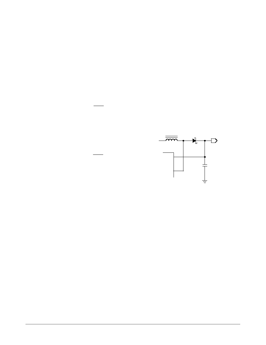
Optional Startup Schottky Diode for Low Battery
Voltage
In general operation, no external schottky diode is
required, however, in case you are intended to operate the
device close to 1.0 V level, a schottky diode connected
between the LX and OUT pins as shown in Figure 27 can
help during startup of the converter. The effect of the
additional schottky is shown in Figure 8.
Figure 27.
C
OUT
V
OUT
L
LX
OUT
NCP1417
MBR0520
PCB Layout Recommendations
Good PCB layout plays an important role in switching
mode power conversion. Careful PCB layout can help to
minimize ground bounce, EMI noise and unwanted
feedback that can affect the performance of the converter.
Hints suggested in below can be used as a guide line in most
situations.
Grounding
Star≠ground connection should be used to connect the
output power return ground, the input power return ground
and the device power ground together at one point. All high
current running paths must be thick enough for current
flowing through and producing insignificant voltage drop
along the path. Feedback signal path must be separated with
the main current path and sensing directly at the anode of the
output capacitor.
Components Placement
Power components, i.e. input capacitor, inductor and
output capacitor, must be placed as close together as
possible. All connecting traces must be short, direct and
thick. High current flowing and switching paths must be
NCP1417
http://onsemi.com
11
kept away from the feedback (FB, pin 1) terminal to avoid
unwanted injection of noise into the feedback path.
Feedback Network
Feedback of the output voltage must be a separate trace
detached from the power path. External feedback network
must be placed very close to the feedback (FB, pin 1) pin and
sensing the output voltage directly at the anode of the output
capacitor.
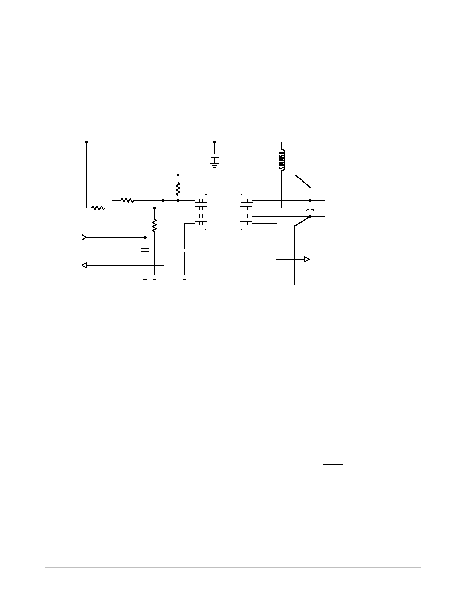
TYPICAL APPLICATION CIRCUIT
Figure 28. Typical Application Schematic for 2 Alkaline Cells Supply
+
33
µ
F
C
OUT
8
7
6
5
1
2
3
4
Input
1 V to
V
OUT
Shutdown
Open Drain
Input
Low Battery
Open Drain
Output 1
308 K
R
LB1
R
FB2
200 K
C
FR1
150 pF
R
FB1
355 K
R
LB2
330 K
150 nF
C
REF
56 nF
C
SHDN
Low Battery
Open Drain
Output 2
V
OUT
= 3.3 V/200 mA max.
22
µ
H
L
10
µ
F
C
IN
NCP1417
LBI/SHDN
LX
LB01
GND
REF
LB02
FB
OUT
GENERAL DESIGN PROCEDURES
Switch mode converter design is considered as black
magic to most engineers, some complicate empirical
formulae are available for reference usage. Those formulae
are derived from the assumption that the key components,
i.e. power inductor and capacitors are available with no
tolerance. Practically, its not true, the result is not a matter
of how accurate the equations you are using to calculate the
component values, the outcome is still somehow away from
the optimum point. Following, is a simple method based on
the most basic first order equations to estimate the inductor
and capacitor values for NCP1417 operating in Continuous
Conduction Mode. The component value set can be used as
a starting point to fine tune the circuit operation. By all
means, detail bench testing is needed to get the best
performance out of the circuit.
Design Parameters:
V
IN
= 1.8 V to 3.0 V, Typical 2.4 V
V
OUT
= 3.3 V
I
OUT
= 150 mA (200 mA max)
V
LB1
= 2.3 V; V
LB2
[ 0.8 V
LB1
= 1.84 V
V
OUT≠RIPPLE
= 40 mV
P≠P
at I
OUT
= 200 mA
Calculate the feedback network:
Select R
FB2
= 200 K
RFB1
+
RFB2
VOUT
VREF
*
1
RFB1
+
200 K
3.3 V
1.19 V
*
1
+
355 K

NCP1417
http://onsemi.com
12
With the feedback resistor divider, additional small
capacitor, C
FB1
in parallel with R
FB1
is required to ensure
stability. The value can be in between 68 nF to 220 nF, the
rule is to select the lowest capacitance to ensure stability.
Also a small capacitor, C
FB2
in parallel with R
FB2
may also
be needed to lower the feedback ripple hence improve
output ripple and regulation. In this example, only C
FB1
is
used and the value is 150 nF.
Calculate the Low Battery Detect divider:
V
LB1
= 2.3 V
Select R
LB2
= 330 K
RLB1
+
RLB2
VLB1
VREF
*
1
RLB1
+
330 K
2.3 V
1.19 V
*
1
+
308 K
Once the V
LB1
is set, the next low battery detection point,
V
LB2
will be fixed automatically.
Determine the Steady State Duty Ratio, D for typical V
IN
,
operation will be optimized around this point:
VOUT
VIN
+
1
1
*
D
D
+
1
*
VIN
VOUT
+
1
*
2.4 V
3.3 V
+
0.273
Determine the average inductor current, I
LAVG
at maximum
I
OUT
:
ILAVG
+
IOUT
1
*
D
+
200 mA
1
*
0.273
+
275 mA
Determine the peak inductor ripple current, I
RIPPLE≠P
and
calculate the inductor value:
Assume I
RIPPLE≠P
is 25% of I
LAVG
, the inductance of the
power inductor can be calculated as follows:
IRIPPLE≠P
+
0.25
275 mA
+
68.8 mA
L
+
VIN
tON
2IRIPPLE≠P
+
2.4 V
1.4
m
S
2(68.8 mA)
+
24.4
m
H
Standard value of 22
mH is selected for initial trial.
Determine the output voltage ripple, V
OUT≠RIPPLE
and
calculate the output capacitor value:
VOUT
*
RIPPLE
+
40 mVP≠P at IOUT
+
200 mA
COUT
u
IOUT
tON
VOUT≠RIPPLE
*
IOUT
ESRCOUT
where tON
+
1.4
m
S and ESRCOUT
+
0.15
W
,
COUT
u
200 mA
1.4
m
S
40 mV
*
200 mA
0.15
W +
28
m
F
From above calculation, you need at least 28
mF in order
to achieve the specified ripple level at conditions stated.
Practically, a one level larger capacitor will be used to
accommodate factors not take into account in the
calculation. So a capacitor value of 33
mF is selected as
initial trial.
NCP1417
http://onsemi.com
13
PACKAGE DIMENSIONS
Micro8
DM SUFFIX
CASE 846A≠02
ISSUE E
S
B
M
0.08 (0.003)
A
S
T
DIM
MIN
MAX
MIN
MAX
INCHES
MILLIMETERS
A
2.90
3.10
0.114
0.122
B
2.90
3.10
0.114
0.122
C
---
1.10
---
0.043
D
0.25
0.40
0.010
0.016
G
0.65 BSC
0.026 BSC
H
0.05
0.15
0.002
0.006
J
0.13
0.23
0.005
0.009
K
4.75
5.05
0.187
0.199
L
0.40
0.70
0.016
0.028
NOTES:
1. DIMENSIONING AND TOLERANCING PER ANSI
Y14.5M, 1982.
2. CONTROLLING DIMENSION: MILLIMETER.
3. DIMENSION A DOES NOT INCLUDE MOLD FLASH,
PROTRUSIONS OR GATE BURRS. MOLD FLASH,
PROTRUSIONS OR GATE BURRS SHALL NOT
EXCEED 0.15 (0.006) PER SIDE.
4. DIMENSION B DOES NOT INCLUDE INTERLEAD
FLASH OR PROTRUSION. INTERLEAD FLASH OR
PROTRUSION SHALL NOT EXCEED 0.25 (0.010)
PER SIDE.
≠B≠
≠A≠
D
K
G
PIN 1 ID
8 PL
0.038 (0.0015)
≠T≠
SEATING
PLANE
C
H
J
L

NCP1417
http://onsemi.com
14
Notes

NCP1417
http://onsemi.com
15
Notes

NCP1417
http://onsemi.com
16
ON Semiconductor and are registered trademarks of Semiconductor Components Industries, LLC (SCILLC). SCILLC reserves the right to make
changes without further notice to any products herein. SCILLC makes no warranty, representation or guarantee regarding the suitability of its products for any
particular purpose, nor does SCILLC assume any liability arising out of the application or use of any product or circuit, and specifically disclaims any and all
liability, including without limitation special, consequential or incidental damages. "Typical" parameters which may be provided in SCILLC data sheets and/or
specifications can and do vary in different applications and actual performance may vary over time. All operating parameters, including "Typicals" must be
validated for each customer application by customer's technical experts. SCILLC does not convey any license under its patent rights nor the rights of others.
SCILLC products are not designed, intended, or authorized for use as components in systems intended for surgical implant into the body, or other applications
intended to support or sustain life, or for any other application in which the failure of the SCILLC product could create a situation where personal injury or death
may occur. Should Buyer purchase or use SCILLC products for any such unintended or unauthorized application, Buyer shall indemnify and hold SCILLC
and its officers, employees, subsidiaries, affiliates, and distributors harmless against all claims, costs, damages, and expenses, and reasonable attorney fees
arising out of, directly or indirectly, any claim of personal injury or death associated with such unintended or unauthorized use, even if such claim alleges that
SCILLC was negligent regarding the design or manufacture of the part. SCILLC is an Equal Opportunity/Affirmative Action Employer.
PUBLICATION ORDERING INFORMATION
JAPAN: ON Semiconductor, Japan Customer Focus Center
4≠32≠1 Nishi≠Gotanda, Shinagawa≠ku, Tokyo, Japan 141≠0031
Phone: 81≠3≠5740≠2700
Email: r14525@onsemi.com
ON Semiconductor Website: http://onsemi.com
For additional information, please contact your local
Sales Representative.
NCP1417/D
Micro8 is a trademark of International Rectifier
Literature Fulfillment:
Literature Distribution Center for ON Semiconductor
P.O. Box 5163, Denver, Colorado 80217 USA
Phone: 303≠675≠2175 or 800≠344≠3860 Toll Free USA/Canada
Fax: 303≠675≠2176 or 800≠344≠3867 Toll Free USA/Canada
Email: ONlit@hibbertco.com
N. American Technical Support: 800≠282≠9855 Toll Free USA/Canada