 | –≠–ª–µ–∫—Ç—Ä–æ–Ω–Ω—ã–π –∫–æ–º–ø–æ–Ω–µ–Ω—Ç: NCP1510 | –°–∫–∞—á–∞—Ç—å:  PDF PDF  ZIP ZIP |

©
Semiconductor Components Industries, LLC, 2003
November, 2003 - Rev. 8
1
Publication Order Number:
NCP1510/D
NCP1510
Advance Information
PWM Buck Converter with a
Very Low Iq During Low
Load Conditions
The NCP1510 is a tri-mode regulator that operates either as a
Synchronized PWM Buck Converter, PWM Buck Converter with
internal oscillator or as a Pulsed Switching Regulator. If a
synchronization signal is present, the NCP1510 operates as a current
mode PWM converter with synchronous rectification. The optional
external frequency input signal allows the user to control the location
of the spurious frequency noise generated by a PWM converter. The
Pulsed Switching Regulator mode is active when the Sync Pin is
Low. The Pulsed Mode is an extremely low quiescent current Buck
Converter. NCP1510 operates in a PWM mode with an internal
oscillator when the Sync Pin is held high. The NCP1510
configuration allows the flexibility of efficient high power operation
and low input current during system sleep modes.
Features
∑
Synchronous Rectification for Higher Efficiency in PWM Mode
∑
Pulsed Switching Mode Operation for Low Current Consumption at
Low Loads
∑
Output Current of 300 mA in PWM and 30 mA in Pulse Mode
∑
Integrated MOSFETs and Feedback Circuits
∑
Cycle-by-Cycle Current Limit
∑
Automatic Switching Between PWM, with External or Internal
Oscillator, and Pulsed Mode
∑
Operating Frequency Range of 450 to 1000 kHz
∑
Internal 1.0 MHz Oscillator
∑
Thermal Limit Protection
∑
Built-in Slope Compensation for Current Mode PWM Converter
∑
1.05, 1.35, 1.57, 1.8 Fixed Output Voltages
∑
Shutdown Current Consumption of 0.2
mA
∑
Pb-Free Package for Green Manufacturing
Applications
∑
Cellular Phones and Pagers
∑
PDA
∑
Digital Cameras
∑
Supplies for DSP Cores
∑
Portable Applications
This document contains information on a new product. Specifications and information
herein are subject to change without notice.
Device
Package
Shipping
{
ORDERING INFORMATION
NCP1510FCT1G
3000 Tape & Reel
9 PIN
MICRO BUMP
FC SUFFIX
CASE 499AC
MARKING
DIAGRAM
PIN CONNECTIONS
(Bottom View)
Pin: A1. - GNDP
A2. - LX
A3. - VCC
B1. - SYNC
B2. - GNDA
B3. - FB
C1. - SHD
C2. - CB1
C3. - CB0
http://onsemi.com
C1
C2
C3
B1
B2
B3
A1
A2
A3
9 Pin Pb-Free
Micro Bump
DAK
YYWW
1
DAK = Device Code
YY = Year
WW = Work Week
G Suffix parts indicate a Pb-Free package and
requires use with a Pb-Free assembly process.
For information on tape and reel specifications,
including part orientation and tape sizes, please
refer to our Tape and Reel Packaging Specifications
Brochure, BRD8011/D.
1

NCP1510
http://onsemi.com
2
Figure 1. Applications Circuit
CB0
Shutdown
Sync
V
out
C
out
10
m
V
bat
CB1
C
in
10
m
L 6.8
m
H
NCP1510
Figure 2. Block Diagram
Sync
V
in
V
out
V
CC
C
in
CB0
SHD
Low Iq
Pulsed
Cntrl
PWM/
PFM
Cntrl
Control
Q1
C
out
FB
L
LX
Q2
GNDA
GNDP
CB1
Bill of Materials
Component
Value
Manufacturer
Part Number
Size (mm)
I
out
(mA)
ESL (m
W
)
C
10
m
F, X5R, 6.3 V
TDK
muRata
C2012X5R0J106
GRM21BR60J106
2.0x1.25x1.25
-
-
L
6.8
m
H
TDK
Coilcraft
Coilcraft
Sumida
LLF4017-6R8
0805PS-682
LPO4812
CLS4D11
4.1x4.0x1.7
3.4x3.0x1.8
4.8x4.8x1.2
4.9x4.9x1.2
700
200
350
600
146
970
230
220
*Output current calculated from VCC = 4.2 Vmax, 1.5 Vout and Freq = 800 kHz (1.0 MHz - 20 %).

NCP1510
http://onsemi.com
3
PIN FUNCTION DESCRIPTION
Pin No.
Symbol
Type
Description
A1
GNDP
Power Ground
Ground Connection for the NFET Power Stage.
A2
LX
Analog Output
Connection from Power Pass Elements to the Inductor.
A3
VCC
Analog Input
Power Supply Input for Power and Analog V
CC
.
B1
SYNC
Analog Input
Synchronization input for the PWM converter. If a clock signal is present, the
converter uses the rising edge for the turn on. If this pin is low, the converter is in
the Pulsed mode. If this pin is high, the converter uses the internal oscillator for the
PWM mode. This pin contains an internal pull down resistor.
B2
GNDA
Analog Ground
Ground connection for the Analog Section of the IC. This is the GND for the FB,
Ref, Sync, CB, and SHD pins.
B3
FB
Analog Input
Feedback Voltage from the Output of the Power Supply.
C1
SHD
Analog Input
Enable for Switching Regulator. This Pin is Active High to enable the NCP1510. The
SDN Pin has an internal pull down resistor to force the converter off if this pin is not
connected to the external circuit.
C2
CB1
Analog Input
Selects V
out
. This pin contains an internal pull up resistor.
C3
CB0
Analog Input
Selects V
out
. This pin contains an internal pull down resistor.
MAXIMUM RATINGS
(Note 1)
Rating
Symbol
Value
Unit
Maximum Voltage All Pins
V
max
5.5
V
Maximum Operating Voltage All Pins
V
max
5.2
V
Thermal Resistance, Junction-to-Air
Rja
159
∞
C/W
Operating Ambient Temperature Range
T
A
-30 to 85
∞
C
ESD Withstand Voltage
Human Body Model (Note 1)
Machine Model (Note 1)
V
ESD
> 2500
> 150
V
Moisture Sensitivity
MSL
Level 1
Storage Temperature Range
T
stg
-55 to 150
∞
C
Junction Operating Temperature
T
J
-30 to 125
∞
C
1. This device series contains ESD protection and exceeds the following tests:
Human Body Model 2,500 V per MIL-STD-883, Method 3015.
Machine Model Method 150 V.

NCP1510
http://onsemi.com
4
ELECTRICAL CHARACTERISTICS
(V
in
= 3.6 V, Vo = 1.57 V, T
A
= 25
∞
C, Fsyn = 600 kHz 50% Duty Cycle square wave for PWM
mode; T
A
= ≠30 to 85
∞
C for Min/Max values, unless otherwise noted.
Characteristic
Symbol
Min
Typ
Max
Unit
VCC Pin
Quiescent Current of Sync Mode, I
out
= 0 mA
Iq PWM
-
175
-
m
A
Quiescent Current of PWM Mode, I
out
= 0 mA
Iq PWM
-
185
-
m
A
Quiescent Current of Pulsed Mode, I
out
= 0 mA
Iq Pulsed
-
14
-
m
A
Quiescent Current, SHD Low
Iq Off
-
0.1
1.0
m
A
Input Voltage Range
Vin
2.5
-
5.2
V
Sync Pin
Input Voltage
Vsync
-0.3
-
Vcc + 0.3
V
Frequency Operational Range
Fsync
450
600
1000
kHz
Minimum Synchronization Pulse Width
Dcsync Min
-
5.0
-
%
Maximum Synchronization Pulse Width
Dcsync Max
-
95
-
%
SYNC "H" Voltage Threshold
Vsynch
-
920
1200
mV
SYNC "L" Voltage Threshold
Vsyncl
400
830
-
mV
SYNC "H" Input Current, Vsync = 3.6 V
Isynch
-
2.2
-
m
A
SYNC "L" Input Current, Vsync = 0 V
Isyncl
-0.5
-
-
m
A
Output Level Selection Pins
Input Voltage
Vcb
-0.3
-
Vcc + 0.3
V
CB0, CB1 "H" Voltage Threshold
Vcb h
-
920
1200
mV
CB0, CB1 "L" Voltage Threshold
Vcb l
400
830
-
mV
CB0 "H" Input Current, CB = 3.6 V
Icb0 h
-
2.2
-
m
A
CB0 "L" Input Current, CB = 0 V
Icb0 l
-0.5
-
-
m
A
CB1 "H" Input Current, CB = 3.6 V
Icb1 h
-
0.3
1.0
m
A
CB1 "L" Input Current, CB = 0 V
Icb1 l
-
-2.2
-
m
A
Shutdown Pin
Input Voltage
Vshd
-0.3
-
Vcc + 0.3
V
SHD "H" Voltage Threshold
Vshd h
-
920
1200
mV
SHD "L" Voltage Threshold
Vshd l
400
830
-
mV
SHD "H" Input Current, SHD = 3.6 V
Ishd h
-
2.2
-
m
A
SHD "L" Input Current, SHD = 0 V
Ishd l
-0.5
-
-
m
A
Feedback Pin
Input Voltage
Vfb
-0.3
-
Vcc + 0.3
V
Input Current, Vfb = 1.5 V
Ifb
-
5.0
7.5
m
A
Sync PWM Mode Characteristics
Switching P-FET Current Limit
I lim
-
800
-
mA
Duty Cycle
DC
-
-
100
%
Minimum On Time
Ton min
-
75
-
nsec
Rdson Switching P-FET and N_FET
Rdson
-
0.23
-
W
Switching P-FET and N-FET Leakage Current
Ileak
-
0
10
m
A
Output Overvoltage Threshold
Vo
-
3.0
-
%
Feedback Voltage Accuracy, V
out
Set = 1.05 V
C
B0
= L, C
B1
= L
V
out
1.018
1.050
1.082
V

NCP1510
http://onsemi.com
5
ELECTRICAL CHARACTERISTICS
(V
in
= 3.6 V, Vo = 1.57 V, T
A
= 25
∞
C, Fsyn = 600 kHz 50% Duty Cycle square wave for PWM
mode; T
A
= ≠30 to 85
∞
C for Min/Max values, unless otherwise noted.
Characteristic
Unit
Max
Typ
Min
Symbol
Sync PWM Mode Characteristics (continued)
Feedback Voltage Accuracy, V
out
Set = 1.35 V, C
B0
= L, C
B1
= H
V
out
1.309
1.350
1.391
V
Feedback Voltage Accuracy, V
out
Set = 1.57 V, C
B0
= H, C
B1
= H
V
out
1.523
1.570
1.617
V
Feedback Voltage Accuracy, V
out
Set = 1.8 V, C
B0
= H, C
B1
= L
V
out
1.746
1.800
1.854
V
Load Transient Response
10 to 100 mA Load Step
V
out
-
-
50
mV
Line Transient Response, I
out
= 100 mA
3.0 to 3.6 Vin Line Step
V
out
-
"
5.0
-
mVpp
PWM Mode with Internal Oscillator Characteristics
Switching P-FET Current Limit
I lim
-
800
-
mA
Duty Cycle
DC
-
-
100
%
Minimum On Time
Ton min
-
75
-
nsec
Internal Oscillator Frequency
Fosc
-
1.0
-
MHz
Rdson Switching P-FET and N_FET
Rdson
-
0.23
-
W
Switching P-FET and N-FET Leakage Current
Ileak
-
0
10
m
A
Output Overvoltage Threshold
Vo
-
3.0
-
%
Feedback Voltage Accuracy, V
out
Set = 1.05 V, C
B0
= L, C
B1
= L
V
out
1.018
1.050
1.082
V
Feedback Voltage Accuracy, V
out
Set = 1.35 V, C
B0
= L, C
B1
= H
V
out
1.309
1.350
1.391
V
Feedback Voltage Accuracy, V
out
Set = 1.57 V, C
B0
= H, C
B1
= H
V
out
1.523
1.570
1.617
V
Feedback Voltage Accuracy, V
out
Set = 1.8 V, C
B0
= H, C
B1
= L
V
out
1.746
1.800
1.854
V
Load Transient Response
10 to 100 mA Load Step
V
out
-
-
50
mV
Line Transient Response, I
out
= 100 mA
3.0 to 3.6 Vin Line Step
V
out
-
"
5.0
-
mVpp
Pulsed Mode Characteristics
On Time
Ton
-
660
-
nsec
Output Current
I
out
0.05
-
30
mA
Output Ripple Voltage, I
out
= 100
m
A
V
out
-
22
100
mV
Feedback Voltage Accuracy, V
out
Set = 1.05 V, C
B0
= L, C
B1
= L
V
out
1.018
1.050
1.082
V
Feedback Voltage Accuracy, V
out
Set = 1.35 V, C
B0
= L, C
B1
= H
V
out
1.309
1.350
1.391
V
Feedback Voltage Accuracy, V
out
Set = 1.57 V, C
B0
= H, C
B1
= H
V
out
1.523
1.570
1.617
V
Feedback Voltage Accuracy, V
out
Set = 1.8 V, C
B0
= H, C
B1
= L
V
out
1.746
1.800
1.854
V

NCP1510
http://onsemi.com
6
INTRODUCTION
The NCP1510 is a tri-mode regulator intended for use in
baseband supplies for portable equipment. Its unique
features provide an efficient power supply for a portable
device at full operating current, while also providing
extremely low standby current for idle mode operation.
When the system is idle, the user can activate the pulsed
mode function. In this mode, the regulator provides a
regulated low current output voltage keeping the system
biased. When the device is in its normal operating mode,
the regulator synchronizes to the system clock or uses an
internal 1.0 MHz clock and turns into a switching
regulator. This allows the regulator to provide efficient
power to the system. This circuit is patent pending.
Operation Description
The Buck regulator is a synchronous rectifier PWM
regulator with integrated MOSFETs. This regulator has a
Pulsed function for low power modes to conserve power.
The Tri PWM with external or internal oscillator/pulsed
mode is an exclusive Patent Pending circuit.
For the PWM Synchronization mode, the operating
frequency range for the NCP1510 is 450 to 1000 kHz. The
output current of the PWM is optimized for 100 mA with
a maximum current supply of over 300 mA for the 2.5 to
5.2 input voltage range.
If the Sync Pin is held low, the NCP1510 changes into the
Pulsed mode. The Pulsed function assures the user of an
extremely low input current and greatly reduced quiescent
current when the users system is in a sleep mode. Internally
to the NCP1510, the Synchronization pin has a pull down
resistor to force the part into Pulsed mode when a clock
signal is not present. The Pulsed mode guarantees an output
of 30 mA.
If the Sync Pin is held high, NCP1510 enters a PWM
mode with an internal 1.0 MHz oscillator. The PWM mode
has the same operational characteristics (current limit,
maximum output current, etc.) as the synchronized PWM
mode. The Sync Pin threshold is fixed as noted in the
Electrical Characteristics table.
Table 1. Sync Pin Input with Corresponding
Operational Mode of NCP1510
Sync Pin State
Operational Mode
Low
Low I
q
Pulsed Mode Operation
High
PWM Using Internal Oscillator for the Clock
Clock
PWM Using Rising Edge of Clock Signal to
Turn On PFET Pass Element
PWM Mode with External Synchronization Signal
During normal operation, a synchronization pulse acts as
the clock for the DC/DC controller. The rising edge of the
clock pulls the gate of Q1 low allowing the inductor to
charge. When the current through Q1 reaches either the
current limit or feedback voltage reaches its limit, Q1 will
turn off and Q2 will turn on. Q2 replaces the free wheeling
diode typically associated with Buck Converters. Q2 will
turn off when either a rising edge sync pulse is present or
all the stored energy is depleted from the inductor.
The output voltage accuracy in the PWM mode is well
within 3% of the nominal set value. An overvoltage
protection circuit is present in the PWM mode to limit the
positive voltage spike due to fast load transient conditions.
If the OVP comparator is activated, the duty cycle will be
0% until the output voltage falls to the nominal level. The
PWM also has the ability to go to 100% duty cycle for
transient conditions and low input to output voltage
differentials.
In PWM mode operates as a forced-PWM converter.
Each switching cycle has a typical on-time of 75nsec.
NCP1510 has two protection circuits that can eliminate the
minimum on time for the cycle. When tripped, the
overvoltage protection or the thermal shutdown overrides
the gate drive of the high side MOSFET.

NCP1510
http://onsemi.com
7
Figure 3. PWM Circuit Schematic
-
+
-
+
-
+
V
bat
C1
10
m
Latch
OC Detect
COMP
OVP
COMP
Error Amp
V
ref
Q2
Q1
L1
6.8
m
H
R3
R4
En Ramp
Set
I
Q1
R1
R2
Sync
Q
S
R
En
C2
10
m
V
ref
+5%
LOAD
400 m
300 m
200 m
400 m
200 m
0.00
Figure 4. Waveforms During PWM Operation
3.6040
V
IN
3.6000
3.5960
400 m
100 m
-200 m
1.01
1.00
990 m
3.70
2.00
-0.30
196.0
201.0
204.0
207.0
210.0
213.0
I
PFET
I
L
I
NFET
V
O
V
LX
TIME (
m
)
PWM Mode with Internal Oscillator
If a synchronization signal is not available, the converter
has a 1.0 MHz internal oscillator available. The Sync Pin
must be held high to enter this mode. The characteristics of
the PWM mode with internal oscillator are similar to the
Sync PWM Mode.
Pulsed Mode
During low-level current output, NCP1510 can enter a
low current consumption mode when the Sync Pin is held
low. This mode will typically have a free running frequency
and an output voltage ripple similar to a PFM mode. The
advantage of the Pulsed mode is much lower Iq (14
mA) and
drastically higher efficiency compared with PWM and
PFM modes in low output loads.

NCP1510
http://onsemi.com
8
0
200
400
600
800
1000
1200
0
200
400
600
800
1000
Figure 5. Input Current Comparison for
V
in
= 3.6 V and V
out
= 1.57 V
I
out
(
m
A)
I
in
(
m
A)
PFM Mode
Pulsed Mode
0
10
20
30
40
50
60
70
80
90
100
0.01
0.1
1
10
100
1000
I
out
(mA)
EFFICIENCY (%)
Figure 6. PWM versus Pulse Efficiency
Comparison
PWM
Pulse
V
CC
= 3.6 V
F
req
PWM = 1.0 MHz
T
A
= 25
∞
C
Figure 7. Converter Efficiency versus Input
Voltage in PWM Mode
INPUT VOLTAGE (V)
EFFICIENCY (%)
78
80
82
84
86
88
90
92
94
96
2.5
3
3.5
4
4.5
5
5.5
1.05 V
OUT
1.35 V
OUT
1.57 V
OUT
1.8 V
OUT
I
out
= 100 mA
F
req
= 1.0 MHz
T
A
= 25
∞
C
Figure 8. Converter Efficiency versus Operational
Frequency in PWM Mode
FREQUENCY (kHz)
EFFICIENCY (%)
400
600
800
1000
1200
1400
1.05 V
OUT
1.35 V
OUT
1.8 V
OUT
1.57 V
OUT
V
CC
= 3.6 V
I
out
= 100 mA
T
A
= 25
∞
C
83
84
85
86
87
88
89
90
91
92
Figure 9. Converter Efficiency versus Output
Current in PWM Mode
I
out
(mA)
EFFICIENCY (%)
60
65
70
75
80
85
90
95
0
100
200
300
400
500
1.8 V
OUT
1.57 V
OUT
1.35 V
OUT
1.05 V
OUT
V
CC
= 3.6 V
F
req
= 1.0 MHz
T
A
= 25
∞
C
Figure 10. Output Voltage versus Output
Current in PWM Mode
0.6
0.8
1.2
2.0
0
200
400
800
I
out
(mA)
V
out
(V)
1.6
1.0
1.4
1.8
600
1.57 V
out
1.35 V
out
1.05 V
out
1.8 V
out
V
CC
= 3.6 V
F
req
= 1.0 MHz
T
A
= 25
∞
C

NCP1510
http://onsemi.com
9
0
0.2
0.4
0.6
0.8
1.2
2.0
0
40
60
120
Figure 11. Output Voltage Delta versus
Output Current in PWM Mode
I
out
(mA)
V
out
(V)
1.6
1.0
1.4
1.8
1.57 V
out
1.35 V
out
1.05 V
out
1.8 V
out
Figure 12. Converter Efficiency versus Input
Current in Pulsed Mode
-30
-25
-20
-15
-10
0
0
20
60
80
Figure 13. Output Voltage versus Output Current
in Pulsed Mode
I
out
(mA)
DEL
T
A
V
out
(V)
10
-5
5
1.57 V
out
1.35 V
out
1.05 V
out
1.8 V
out
-5
0
10
30
0
200
400
800
I
out
(mA)
DEL
T
A
V
out
(V)
20
5
15
25
600
1.57 V
out
1.35 V
out
1.05 V
out
1.8 V
out
-20
-15
-10
20
80
100
40
V
CC
= 3.6 V
F
req
= 1.0 MHz
T
A
= 25
∞
C
V
CC
= 3.6 V
T
A
= 25
∞
C
V
CC
= 3.6 V
T
A
= 25
∞
C
5
4
3
2
1
0
V
SHD
(V)
I
SH
D
(
m
A)
2.5
2
1.5
1
0.5
0
V
CC
= 3.6 V
T
A
= 25
∞
C
4
3
2
1
0
V
SYN
(V)
I
SYN
(
m
A)
2
1.8
1.2
1
0.2
0
V
CC
= 3.6 V
T
A
= 25
∞
C
0.4
0.6
0.8
1.4
1.6
Figure 14. Output Voltage Delta versus
Output Current in Pulsed Mode
Figure 15. Input Current versus Voltage for the
Shutdown Pin
0
10
20
30
40
50
60
0.01
0.1
1
10
100
I
out
(mA)
EFFICIENCY (%)
1.57 V
out
1.35 V
out
1.05 V
out
70
80
90
100
1.8 V
out
V
CC
= 3.6 V
T
A
= 25
∞
C
Figure 16. Input Current versus Voltage for the
Synchronization Pin

NCP1510
http://onsemi.com
10
Figure 17. Input Current versus Voltage for CB0
4
3
2
1
0
V
CB
(V)
I
CB
0
(
m
A)
2.5
2
1.5
1
0.5
0
V
CC
= 3.6 V
T
A
= 25
∞
C
Figure 18. Input Current versus Input Voltage
for CB1
2
1.5
1
0.5
0
V
FB
(V)
I
FB
(
m
A)
8
7
4
3
0
-1
V
CC
= 3.6 V
T
A
= 25
∞
C
PWM Mode
1
2
5
6
Figure 19. Input Current versus Voltage for the
Feedback Pin
4
3
2
1
0
V
CB1
(V)
I
CB
1
(
m
A)
1
0.5
0
-0.5
-2
-2.5
-1.5
-1
V
CC
= 3.6 V
T
A
= 25
∞
C

NCP1510
http://onsemi.com
11
V
th
Low
Figure 20. V
CC
Input Voltage versus CB
Threshold
6
5
4
3
2
V
CC
(V)
V
C
B
(t
hres
hold)
(V)
0.93
0.89
0.88
0.85
0.84
T
A
= 25
∞
C
PWM Mode
0.87
0.86
0.92
0.91
0.90
V
th
High
Figure 21. Transition Level of CB Pins
1.4
0.6
0.4
0.2
0
V
CB
(V)
V
out
(V)
1.55
1.5
1.4
1.3
1.35
1.45
1.2
1.0
0.8
1.6
V
CC
= 3.6 V
T
A
= 25
∞
C
Figure 22. Input Voltage versus Shutdown Voltage
Figure 23. Output Voltage versus Shutdown Pin
Voltage
6
5
4
3
2
V
CC
(V)
V
SH
D
(
t
h
res
hold)
(V)
0.93
0.89
0.88
0.85
0.84
T
A
= 25
∞
C
1.4
0.6
0.4
0.2
0
V
SHD
(V)
V
out
(V)
1.8
T
A
= 25
∞
C
0
0.87
0.86
0.92
0.91
0.90
V
SHD
High
1.2
1.0
0.8
V
SHD
Low
V
SHD
Decreasing
V
SHD
Increasing
Figure 24. PWM Mode to Pulsed Mode
Transition
Figure 25. Pulsed Mode to PWM Mode
Transition
SYNC Pin
V
OUT
V
CC
= 3.6 V, I
OUT
= 10 mA, T
A
= 25
∞
C
V
CC
= 3.6 V, I
OUT
= 10 mA, T
A
= 25
∞
C
SYNC Pin
V
OUT

NCP1510
http://onsemi.com
12
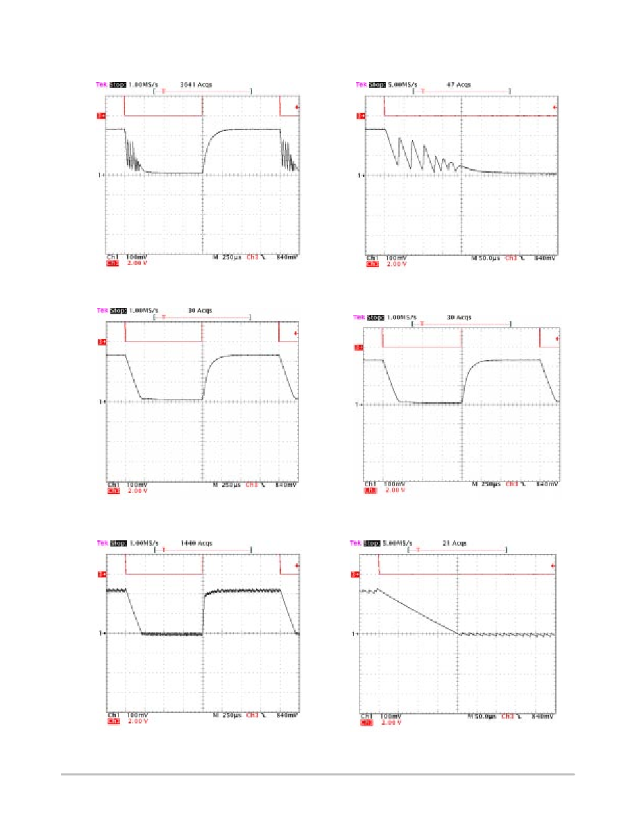
Figure 26. PWM Startup Inrush Current ≠
400
W
Load, 1.57 V
out
Figure 27. PWM Startup Inrush Current ≠
400
W
Load, 1.57 V
out
Figure 28. PWM Startup Inrush Current ≠
10
W
Load, 1.57 V
out
Figure 29. Pulse Startup Inrush Current ≠
400
W
Load, 1.57 V
out
Figure 30. Pulse Startup Inrush Current ≠
400
W
Load, 1.57 V
out
Figure 32. Pulse Startup Inrush Current ≠
25
W
Load, 1.57 V
out
INRUSH CURRENT MEASUREMENTS
CH4: Iin (20 mA/div)
SDN Pin
V
OUT
Iin
SDN Pin
V
OUT
Iin
SDN Pin
V
OUT
Iin
SDN Pin
V
OUT
Iin
SDN Pin
V
OUT
Iin
SDN Pin
V
OUT
Iin
NCP1510
http://onsemi.com
13
Figure 33. PWM DVM ≠ 30
W
Load, 1.35 to 1.57 V
out
Figure 34. PWM DVM ≠ 30
W
Load, 1.35 to 1.57 V
out
Figure 35. PWM DVM ≠ 150
W
Load, 1.35 to 1.57 V
out
DYNAMIC VOLTAGE MANAGEMENT
Figure 36. PWM DVM ≠ 150
W
Load, 1.35 to 1.57 V
out
Figure 37. Pulse DVM ≠ 150
W
Load, 1.35 to 1.57 V
out
Figure 38. Pulse DVM ≠ 150
W
Load, 1.35 to 1.57 V
out
CB0
V
OUT
CB0
V
OUT
CB0
V
OUT
CB0
V
OUT
CB0
V
OUT
CB0
V
OUT

NCP1510
http://onsemi.com
14
Voltage Output Selection
The CB1 and CB0 pins control the output voltage
selection. The output voltages are listed in Table 2. The CB
pins contain internal resistors to force the NCP1510 to 1.35
V
out
if they are not connected to an external circuit. The
CB0 has a pull down resistor and the CB1 has a pull up
resistor. The CB Pin thresholds are fixed as noted in the
Electrical Characteristics table.
Shutdown Pin
The Shutdown Pin enables the operation of the device.
The Shutdown Pin has an internal pull down resistor to
force the NCP1510 into the off mode if this pin is floating
due to the external circuit. The Shutdown Pin threshold is
fixed as noted in the Electrical Characteristics table.
During Start-up, the NCP1510 has a soft start function to
limit fast dV/dt and eliminate overshoot on the output.
Thermal Shutdown
Internal Thermal Shutdown circuitry is provided to
protect the integrated circuit in the event at the maximum
junction temperature is exceeded. When activated,
typically at 16
0
∞
C, the PWM latch is reset and the linear
regulator control circuitry is disabled. The thermal
shutdown circuit is designed with 2
5
∞
C of hysteresis. This
means that the PWM latch and the regulator control
circuitry cannot be re≠enabled until the die temperature
drops by this amount. This feature is provided to prevent
catastrophic failures from accidental device overheating.
It is not intended as a substitute for proper heat-sinking.
The NCP1510 is contained in a 9 pin micro bump package.
Table 2. Truth Table for CB0 and CB1 with the
Corresponding Output Voltage
CB0
CB1
V
out
(V)
0
0
1.05
0
1
1.35
1
1
1.57
1
0
1.8

NCP1510
http://onsemi.com
15
PACKAGE DIMENSIONS
RECOMMENDED PCB FOOTPRINT
0.250
0.280
0.5
0.5
9 PIN MICRO BUMP
FC SUFFIX
CASE 499AC-01
ISSUE O
NOTE:
Use a Pb-Free Solder Paste, such as Omnix 310 89-3-M11, with the Pb-Free package (G Suffix).
DIM
MIN
MAX
MILLIMETERS
A
0.540
0.660
A1
0.210
0.270
A2
NOTES:
1. DIMENSIONING AND TOLERANCING PER
ANSI Y14.5M, 1982.
2. CONTROLLING DIMENSION: MILLIMETERS.
3. COPLANARITY APPLIES TO SPHERICAL
CROWNS OF SOLDER BALLS.
E
D
-A-
-B-
0.10 C
A2
A
A1
-C-
0.05 C
0.10 C
4 X
SEATING
PLANE
D1
e
E1
e
0.05 C
0.03 C
A B
9 X
b
C
B
A
1
2
3
D
1.550 BSC
E
0.330
0.390
b
0.290
0.340
e
0.500 BSC
D1
1.000 BSC
E1
1.000 BSC
1.550 BSC

NCP1510
http://onsemi.com
16
ON Semiconductor and are registered trademarks of Semiconductor Components Industries, LLC (SCILLC). SCILLC reserves the right to make changes without further notice
to any products herein. SCILLC makes no warranty, representation or guarantee regarding the suitability of its products for any particular purpose, nor does SCILLC assume any
liability arising out of the application or use of any product or circuit, and specifically disclaims any and all liability, including without limitation special, consequential or incidental
damages. "Typical" parameters which may be provided in SCILLC data sheets and/or specifications can and do vary in different applications and actual performance may vary over
time. All operating parameters, including "Typicals" must be validated for each customer application by customer's technical experts. SCILLC does not convey any license under
its patent rights nor the rights of others. SCILLC products are not designed, intended, or authorized for use as components in systems intended for surgical implant into the body,
or other applications intended to support or sustain life, or for any other application in which the failure of the SCILLC product could create a situation where personal injury or death
may occur. Should Buyer purchase or use SCILLC products for any such unintended or unauthorized application, Buyer shall indemnify and hold SCILLC and its officers, employees,
subsidiaries, affiliates, and distributors harmless against all claims, costs, damages, and expenses, and reasonable attorney fees arising out of, directly or indirectly, any claim of
personal injury or death associated with such unintended or unauthorized use, even if such claim alleges that SCILLC was negligent regarding the design or manufacture of the part.
SCILLC is an Equal Opportunity/Affirmative Action Employer. This literature is subject to all applicable copyright laws and is not for resale in any manner.
PUBLICATION ORDERING INFORMATION
N. American Technical Support: 800-282-9855 Toll Free
USA/Canada
Japan: ON Semiconductor, Japan Customer Focus Center
2-9-1 Kamimeguro, Meguro-ku, Tokyo, Japan 153-0051
Phone: 81-3-5773-3850
NCP1510/D
LITERATURE FULFILLMENT:
Literature Distribution Center for ON Semiconductor
P.O. Box 5163, Denver, Colorado 80217 USA
Phone: 303-675-2175 or 800-344-3860 Toll Free USA/Canada
Fax: 303-675-2176 or 800-344-3867 Toll Free USA/Canada
Email: orderlit@onsemi.com
ON Semiconductor Website: http://onsemi.com
Order Literature: http://www.onsemi.com/litorder
For additional information, please contact your
local Sales Representative.