 | –≠–ª–µ–∫—Ç—Ä–æ–Ω–Ω—ã–π –∫–æ–º–ø–æ–Ω–µ–Ω—Ç: NCP1511 | –°–∫–∞—á–∞—Ç—å:  PDF PDF  ZIP ZIP |
©
Semiconductor Components Industries, LLC, 2005
January, 2005 - Rev. 5
1
Publication Order Number:
NCP1511/D
NCP1511
Up to 500 mA, High
Efficiency Synchronous
Step-Down DC-DC Converter
in Chip Scale Package
The NCP1511 step-down PWM DC-DC converter is optimized
for portable applications powered from 1-cell Li-ion or 3-cell
Alkaline/NiCd/NiMH batteries. This DC-DC converter utilizes a
current-mode control architecture for easy compensation and better
line regulation. It also uses synchronous rectification to increase
efficiency and reduce external part count. The NCP1511 optimizes
efficiency in light load conditions when switched from a normal
PWM mode to a "pulsed switching" mode. The device also has a
built-in oscillator for the PWM circuitry, or it can be synchronized to
an external 500 kHz to 1000 kHz clock signal. Finally, it includes an
integrated soft-start, cycle-by-cycle current limiting, and thermal
shutdown protection. The NCP1511 is available in a chip scale
package.
Features
∑
High Efficiency:
93% for 1.89 V Output at 3.6 V Input and 150 mA Load Current
92% for 1.89 V Output at 3.6 V Input and 300 mA Load Current
∑
Digital Programmable Output Voltages: 1.0, 1.3, 1.5 or 1.89 V
∑
Output Current up to 500 mA at V
in
= 3.6 V
∑
Low Quiescent Current of 14
mA in Pulsed Switching Mode
∑
Low 0.1
mA Shutdown Current
∑
-30
∞
C to 85
∞
C Operation Temperature
∑
Ceramic Input/Output Capacitor
∑
9 Pin Chip Scale Package
∑
Pb-Free Package is Available
Applications
∑
Cellular Phones, Smart Phones and PDAs
∑
Digital Still Cameras
∑
MP3 Players and Portable Audio Systems
∑
Wireless and DSL Modems
∑
Portable Equipment
DAL
AYWW
A1
http://onsemi.com
Device
Package
Shipping
ORDERING INFORMATION
NCP1511FCT1
3000 Tape & Reel
9 PIN
MICRO BUMP
FC SUFFIX
CASE 499AC
MARKING
DIAGRAM
Micro Bump
XX = Device Code
A
= Assembly Location
Y
= Year
WW = Work Week
C1
C2
C3
B1
B2
B3
A1
A2
A3
Pin: A1. - GNDP
A2. - LX
A3. - VCC
B1. - SYNC
B2. - GNDA
B3. - FB
C1. - SHD
C2. - CB1
C3. - CB0
(Bottom View)
PIN CONNECTIONS
NCP1511FCT1G
3000 Tape & Reel
Micro Bump
(Pb-Free)
A1
For information on tape and reel specifications,
including part orientation and tape sizes, please
refer to our Tape and Reel Packaging Specifications
Brochure, BRD8011/D.
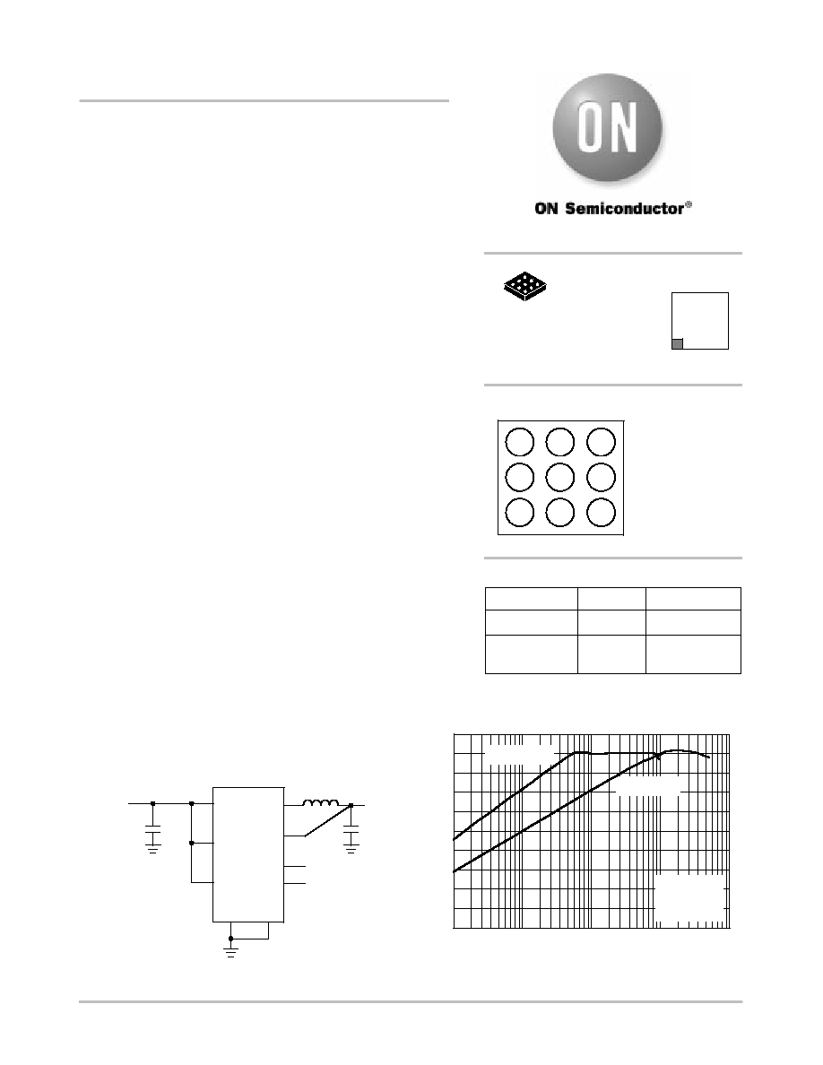
Figure 1. Typical Application Circuit
VCC
SHD
SYNC
GNDA GNDP
CB0
CB1
FB
LX
V
in
2.5 V - 5.2 V
6.8
m
H
V
out
CB0 and CB1
Control Input
C
in
10
m
F
C
out
22
m
F
A3
C1
B1
B2
A1
C3
C2
B3
A2
0
10
20
30
40
50
60
70
80
90
100
0.1
1
10
100
1000
PWM Mode
Pulsed Mode
EFFICIENCY
(
%
)
I
out
(mA)
Figure 2. Efficiency vs. Output Current
V
in
= 3.6 V
V
out
= 1.5 V
T
A
= 25
∞
C
NCP1511
http://onsemi.com
2
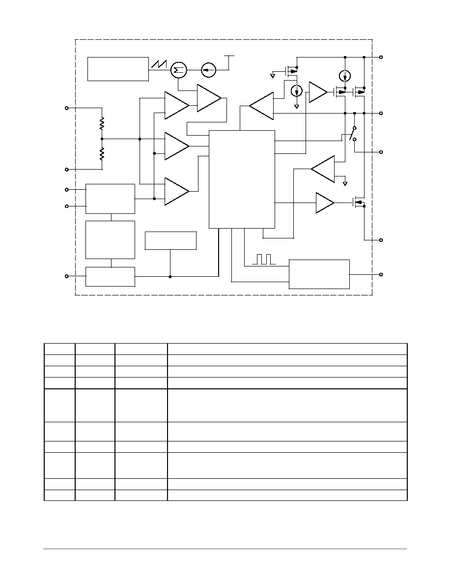
Figure 3. Simplified Block Diagram
+
-
-
+
+
-
+
-
+
-
+
-
FB
GNDA
CB0
CB1
SHD
ISENS
ISENS
SENFET
ILIM
ZCL
MODE SELECTION
SYNC DETECT
AND
TIMING BLOCK
SYNC DETECT
AND
TIMING BLOCK
THERMAL
SHUTDOWN
ENABLE
DETECT
SELECT
LOGIC
BANDGAP
REFERENCE
AND SOFT
START
PWM
OVP
PM
CMP
CMP
CMP
CMP
CMP
OA
Q2
Q1
DVR
DVR
COMPENSATION
RAMP
CONTROL
BLOCK
(PWM,PM)
GNDP
SYNC
LX
VCC
FB
DAMPING
SWITCHING
CONTROL
DAMPING
SWITCHING
CONTROL
PIN FUNCTION DESCRIPTION
Pin No.
Symbol
Type
Description
A1
GNDP
Power Ground
Ground Connection for the NFET Power Stage.
A2
LX
Analog Output
Connection from Power Pass Elements to the Inductor.
A3
V
CC
Analog Input
Power Supply Input for Power and Analog V
CC
.
B1
SYNC
Analog Input
Synchronization input for the PWM converter. If a clock signal is present, the converter
uses the rising edge for the turn on. If this pin is low, the converter is in the Pulsed mode.
If this pin is high, the converter uses the internal oscillator for the PWM mode. This pin
contains an internal pull down resistor.
B2
GNDA
Analog Ground
Ground connection for the Analog Section of the IC. This is the GND for the FB, Ref,
Sync, CB, and SHD pins.
B3
FB
Analog Input
Feedback Voltage from the Output of the Power Supply.
C1
SHD
Analog Input
Enable for Switching Regulator. This Pin is Active High to enable the NCP1511. The SHD
Pin has an internal pull down resistor to force the converter off if this pin is not connected
to the external circuit.
C2
CB1
Analog Input
Selects V
out
. This pin contains an internal pull up resistor.
C3
CB0
Analog Input
Selects V
out
. This pin contains an internal pull down resistor.
NCP1511
http://onsemi.com
3
MAXIMUM RATINGS
Rating
Symbol
Value
Unit
Maximum Voltage All Pins
V
max
5.5
V
Maximum Operating Voltage All Pins
V
max
5.2
V
Thermal Resistance, Junction-to-Air (Note 1)
R
q
JA
159
∞
C/W
Operating Ambient Temperature Range
T
A
-30 to 85
∞
C
ESD Withstand Voltage
Human Body Model (Note 2)
Machine Model (Note 2)
V
ESD
> 2500
> 150
V
Moisture Sensitivity
MSL
Level 1
Storage Temperature Range
T
stg
-55 to 150
∞
C
Junction Operating Temperature
T
J
-30 to 125
∞
C
Maximum ratings are those values beyond which device damage can occur. Maximum ratings applied to the device are individual stress limit values
(not normal operating conditions) and are not valid simultaneously. If these limits are exceeded, device functional operation is not implied, damage
may occur and reliability may be affected.
1. For the 9-Pin Micro Bump package, the R
q
JA
is highly dependent of the PCB heatsink area. R
q
JA
= 159
∞
C/W with 50 mm
2
PCB heatsink area.
2. This device series contains ESD protection and exceeds the following tests:
Human Body Model, 100 pF discharge through a 1.5 k
W
following specification JESD22/A114.
Machine Model, 200 pF discharged through all pins following specification JESD22/A115.
Latchup as per JESD78 Class II: > 100 mA.
NCP1511
http://onsemi.com
4
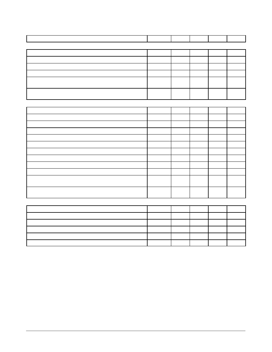
ELECTRICAL CHARACTERISTICS
(V
in
= 3.6 V, Vo = 1.5 V, T
A
= 25
∞
C, Fsyn = 600 kHz 50% Duty Cycle square wave for PWM
mode; T
A
= ≠30 to 85
∞
C for Min/Max values, unless otherwise noted.
Characteristic
Symbol
Min
Typ
Max
Unit
VCC Pin
Quiescent Current of Sync Mode, I
out
= 0 mA
Iq PWM
-
175
-
m
A
Quiescent Current of PWM Mode, I
out
= 0 mA
Iq PWM
-
185
-
m
A
Quiescent Current of Pulsed Mode, I
out
= 0 mA
Iq Pulsed
-
14
-
m
A
Quiescent Current, SHD Low
Iq Off
-
0.1
0.5
m
A
Input Voltage Range (Note 3)
Vin
2.5
-
5.2
V
Sync Pin
Input Voltage
Vsync
-0.3
-
Vcc + 0.3
V
Frequency Operational Range
Fsync
500
600
1000
kHz
Minimum Synchronization Pulse Width
Dcsync Min
-
30
-
%
Maximum Synchronization Pulse Width
Dcsync Max
-
70
-
%
SYNC "H" Voltage Threshold
Vsynch
-
920
1200
mV
SYNC "L" Voltage Threshold
Vsyncl
400
830
-
mV
SYNC "H" Input Current, Vsync = 3.6 V
Isynch
-
2.2
-
m
A
SYNC "L" Input Current, Vsync = 0 V
Isyncl
-0.5
-
-
m
A
Output Level Selection Pins
Input Voltage
Vcb
-0.3
-
Vcc + 0.3
V
CB0, CB1 "H" Voltage Threshold
Vcb h
-
920
1200
mV
CB0, CB1 "L" Voltage Threshold
Vcb l
400
830
-
mV
CB0 "H" Input Current, CB = 3.6 V
Icb0 h
-
2.2
-
m
A
CB0 "L" Input Current, CB = 0 V
Icb0 l
-0.5
-
-
m
A
CB1 "H" Input Current, CB = 3.6 V
Icb1 h
-
0.3
1.0
m
A
CB1 "L" Input Current, CB = 0 V
Icb1 l
-
-2.2
-
m
A
Shutdown Pin
Input Voltage
Vshd
-0.3
-
Vcc + 0.3
V
SHD "H" Voltage Threshold
Vshd h
-
920
1200
mV
SHD "L" Voltage Threshold
Vshd l
400
830
-
mV
SHD "H" Input Current, SHD = 3.6 V
Ishd h
-
2.2
-
m
A
SHD "L" Input Current, SHD = 0 V
Ishd l
-0.5
-
-
m
A
Feedback Pin
Input Voltage
Vfb
-0.3
-
Vcc + 0.3
V
Input Current, Vfb = 1.5 V
Ifb
-
5.0
7.5
m
A
Sync PWM Mode Characteristics
Switching P-FET Current Limit
I lim
-
800
-
mA
Minimum On Time
Ton min
-
75
-
nsec
Rdson Switching P-FET and N_FET
Rdson
-
0.23
-
W
Switching P-FET and N-FET Leakage Current
Ileak
-
0
1.0
m
A
Output Overvoltage Threshold
Vo
-
5.0
-
%
3. Recommended maximum input voltage is 5 V when the device frequency is synchronized with an external clock signal.
NCP1511
http://onsemi.com
5
ELECTRICAL CHARACTERISTICS (continued)
(V
in
= 3.6 V, Vo = 1.5 V, T
A
= 25
∞
C, Fsyn = 600 kHz 50% Duty Cycle square wave
for PWM mode; T
A
= ≠30 to 85
∞
C for Min/Max values, unless otherwise noted.
Characteristic
Symbol
Min
Typ
Max
Unit
Sync PWM Mode Characteristics (continued)
Feedback Voltage Accuracy, V
out
Set = 1.0 V CB0 = L, CB1 = L
V
out
0.950
1.000
1.050
V
Feedback Voltage Accuracy, V
out
Set = 1.3 V CB0 = L, CB1 = H
V
out
1.261
1.300
1.339
V
Feedback Voltage Accuracy, V
out
Set = 1.5 V CB0 = H, CB1 = H
V
out
1.450
1.500
1.550
V
Feedback Voltage Accuracy, V
out
Set = 1.89 V CB0 = H CB1 = L
V
out
1.833
1.890
1.947
V
Load Transient Response
10 to 100 mA Load Step
V
out
-
35
-
mV
Line Transient Response, I
out
= 100 mA
3.0 to 3.6 Vin Line Step
V
out
-
"
10
-
mVpp
PWM Mode with Internal Oscillator Characteristics
Switching P-FET Current Limit
I lim
-
800
-
mA
Minimum On Time
Ton min
-
75
-
nsec
Internal Oscillator Frequency
Fosc
700
900
1200
kHz
Rdson Switching P-FET and N_FET
Rdson
-
0.23
-
W
Switching P-FET and N-FET Leakage Current
Ileak
-
0
1.0
m
A
Output Overvoltage Threshold
Vo
-
5.0
-
%
Feedback Voltage Accuracy, V
out
Set = 1.0 V CB0 = L, CB1 = L
V
out
0.950
1.000
1.050
V
Feedback Voltage Accuracy, V
out
Set = 1.3 V CB0 = L, CB1 = H
V
out
1.261
1.300
1.339
V
Feedback Voltage Accuracy, V
out
Set = 1.5 V CB0 = H, CB1 = H
V
out
1.450
1.500
1.550
V
Feedback Voltage Accuracy, V
out
Set = 1.89 V CB0 = H CB1 = L
V
out
1.833
1.890
1.947
V
Load Transient Response
10 to 100 mA Load Step
V
out
-
35
-
mV
Line Transient Response, I
out
= 100 mA
3.0 to 3.6 Vin Line Step
V
out
-
"
10
-
mVpp
Pulsed Mode Characteristics
On Time
Ton
-
660
-
nsec
Output Ripple Voltage, I
out
= 100
m
A
V
out
-
22
-
mV
Feedback Voltage Accuracy, V
out
Set = 1.0 V CB0 = L, CB1 = L
V
out
0.930
1.000
1.070
V
Feedback Voltage Accuracy, V
out
Set = 1.3 V CB0 = L, CB1 = H
V
out
1.241
1.300
1.359
V
Feedback Voltage Accuracy, V
out
Set = 1.5 V CB0 = H, CB1 = H
V
out
1.430
1.500
1.570
V
Feedback Voltage Accuracy, V
out
Set = 1.89 V CB0 = H CB1 = L
V
out
1.813
1.890
1.967
V
NCP1511
http://onsemi.com
6
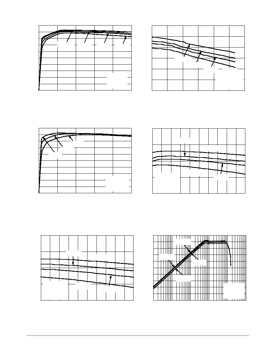
Figure 4. Efficiency vs. Output Current in PWM
Mode
70
75
80
85
90
95
100
2.5
3.0
3.5
4.0
4.5
5.5
EFFICIENCY
(
%
)
INPUT VOLTAGE (V)
Figure 5. Efficiency vs. Input Voltage in PWM
Mode
I
out
= 150 mA
Freq = 1.0 MHz
T
A
= 25
∞
C
Figure 6. Efficiency vs. Output Current at
Different Input Voltage
80
85
90
95
100
500 600
800
1000
1200
1400
1.0 V
out
1.3 V
out
1.5 V
out
1.89 V
out
FREQUENCY (kHz)
Figure 7. Efficiency vs. Frequency at
I
out
= 150 mA
V
in
= 3.6 V
I
out
= 150 mA
T
A
= 25
∞
C
PWM
Figure 8. Efficiency vs. Frequency at
I
out
= 300 mA
EFFICIENCY
(
%
)
Figure 9. Efficiency vs. Output Current in
Pulsed Mode
0
10
20
30
40
50
60
70
0
100
200
300
400
500
EFFICIENCY
(
%
)
I
out
(mA)
80
90
100
1.0 V
out
1.3 V
out
1.5 V
out
1.89 V
out
0
10
20
30
40
50
60
70
0
100
200
300
400
500
5.2 V
in
3.6 V
in
2.7 V
in
EFFICIENCY
(
%
)
I
out
(mA)
V
out
= 1.5 V
PWM
T
A
= 25
∞
C
80
90
100
700
900
1100
1300
1500
80
85
90
95
100
500 600
800
1000
1200
1400
1.0 V
out
1.3 V
out
1.5 V
out
1.89 V
out
FREQUENCY (kHz)
V
in
= 3.6 V
I
out
= 300 mA
T
A
= 25
∞
C
PWM
EFFICIENCY
(
%
)
700
900
1100
1300
1500
0
10
20
30
40
50
60
70
80
90
100
0.01
1
10
100
1000
EFFICIENCY
(
%
)
I
out
(mA)
V
in
= 3.6 V
PM
T
A
= 25
∞
C
1.0 V
out
1.3 V
out
1.5 V
out
1.89 V
out
0.1
5.0
1.0 V
out
1.3 V
out
1.5 V
out
1.89 V
out
V
in
= 3.6 V
PWM
T
A
= 25
∞
C
NCP1511
http://onsemi.com
7
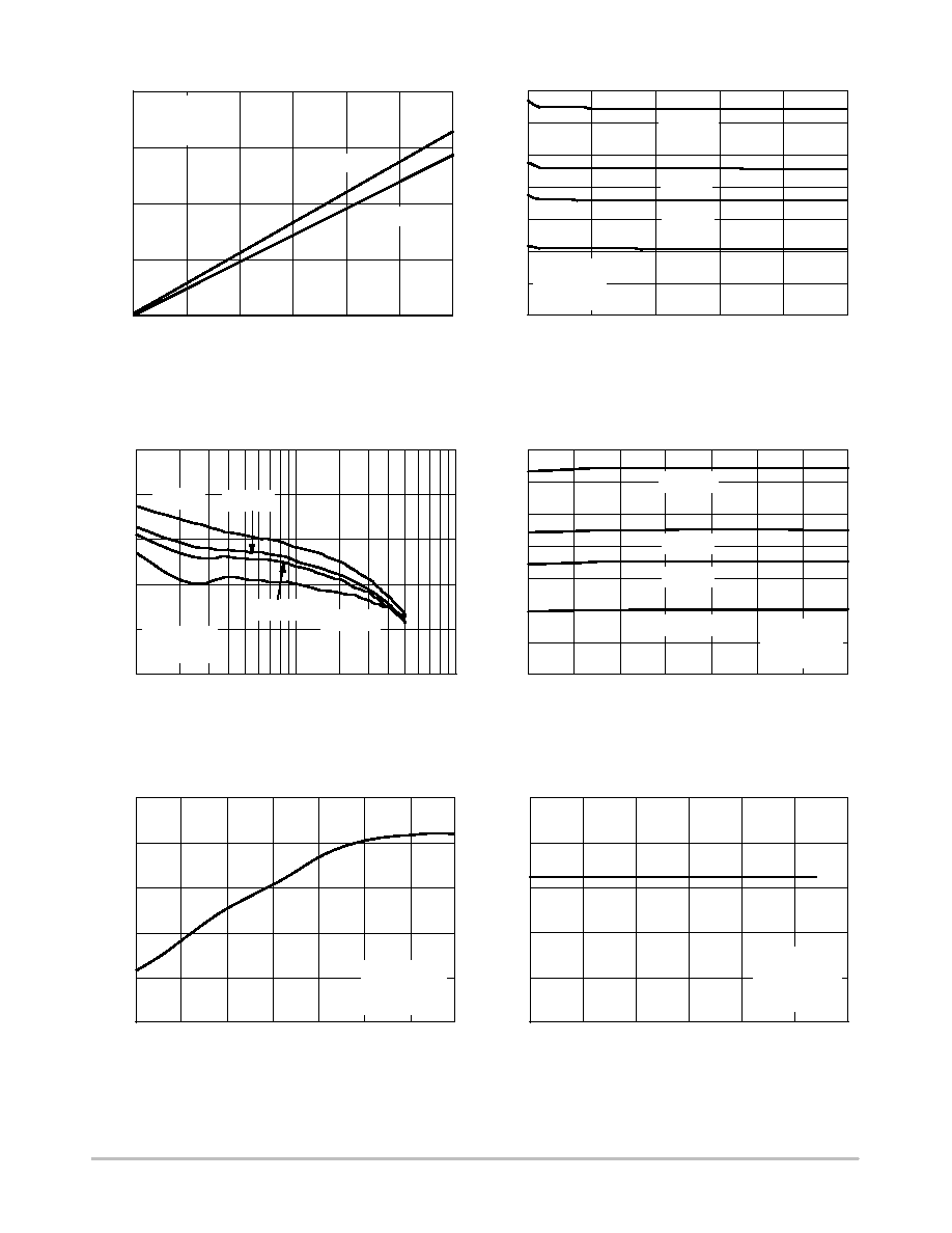
Figure 10. Input Current Comparison
0.6
0.8
1
1.2
1.4
1.6
1.8
2
0
100
200
300
400
500
V
in
= 3.6 V
T
A
= 25
∞
C
PWM
V
out
(V)
Figure 11. Output Voltage vs. Output Current
1.0 V
out
1.3 V
out
1.5 V
out
1.89 V
out
I
out
(mA)
1000
100
10
I
out
(mA)
D
V
out
(mV)
15
10
5
0
-5
-10
V
in
= 3.6 V
T
A
= 25
∞
C
Figure 12. Load Regulation in PWM Mode
40
100
20
-20
-40
TEMPERATURE (
∞
C)
V
out
(V)
2
1.8
1.2
1
V
in
= 3.6 V
I
out
= 150 mA
PWM
0.6
0.8
1.4
1.6
Figure 13. Output Voltage vs. Temperature
Figure 14. Oscillator Frequency vs. Temperature
Figure 15. Oscillator Frequency vs. Input
Voltage
V
in
(V)
FREQUENCY (kHz)
1.89 V
out
1.0 V
out
1.3 V
out
1.5 V
out
0
80
60
1.89 V
out
1.5 V
out
1.3 V
out
1.0 V
out
40
100
20
-20
-40
TEMPERATURE (
∞
C)
FREQUENCY (kHz)
910
890
850
870
950
0
80
60
V
in
= 3.6 V
V
out
= 1.5 V
I
out
= 150 mA
850
870
890
910
930
950
2.5
3.0
3.5
4.0
4.5
5.5
V
out
= 1.5 V
I
out
= 150 mA
T
A
= 25
∞
C
PWM
0
5
10
0
5
10
15
20
30
I
out
(mA)
I
in
(
m
A)
PWM Mode
Pulsed Mode
25
15
20
V
in
= 3.6 V
V
out
= 1.5 V
T
A
= 25
∞
C
5.0
930
NCP1511
http://onsemi.com
8
V
CB
(V)
Figure 16. Output Voltage vs. Shutdown Pin
Voltage
1.4
0.6
0.4
0.2
0
V
SHD
(V)
V
out
(V)
2.0
1.5
1.0
0
0.5
1.2
1.0
0.8
Figure 17. Transition Level of CB Pins
V
in
= 3.6 V
V
out
= 1.5 V
T
A
= 25
∞
C
PWM Mode
1.4
0.6
0.4
0.2
0
V
out
(V)
2.0
1.5
1.0
0
0.5
1.2
1.0
0.8
V
in
= 3.6 V
V
out
= 1.5 V
T
A
= 25
∞
C
PWM Mode
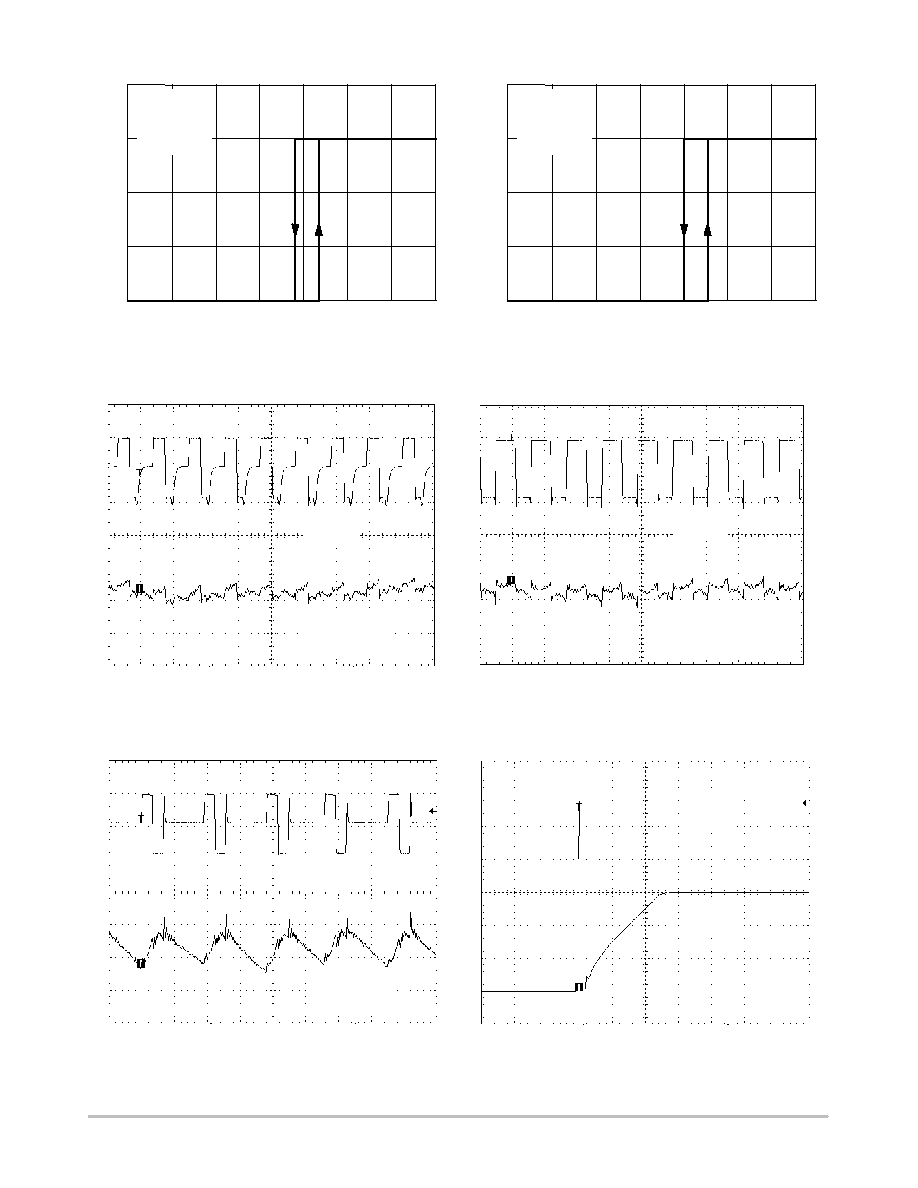
Figure 18. Light Load PWM Switching Waveform
(V
in
= 3.6 V, V
out
= 1.5 V, I
out
= 30 mA)
Figure 19. Heavy Load PWM Switching Waveform
(V
in
= 3.6 V, V
out
= 1.5 V, I
out
= 300 mA)
Figure 20. Pulsed Mode Switching Waveform
(V
in
= 3.6 V, V
out
= 1.5 V, I
out
= 30 mA)
Figure 21. Soft-Start
(V
in
= 3.6 V, V
out
= 1.5 V, I
out
= 150 mA)
1
m
s/div
V
out
AC Coupled
10 mV/div
V
LX
1 V/div
1
m
s/div
V
out
AC Coupled
10 mV/div
V
LX
1 V/div
500 ms/div
V
out
0.5 V/div
V
shdn
1 V/div
1
m
s/div
V
out
AC Coupled
10 mV/div
V
LX
1 V/div
1.5 V
2 V
0
0
NCP1511
http://onsemi.com
9
Figure 22. Line Transient Response for PWM
Figure 23. Line Transient Response for PM
200
m
s/div
V
out
AC Coupled
10 mV/div
V
in
1 V/div
V
out
= 1.89 V
I
out
= 300 mA
PWM
3.0 V
3.6 V
200
m
s/div
V
out
AC Coupled
10 mV/div
V
in
1 V/div
V
out
= 1.89 V
I
out
= 30 mA
PM
3.0 V
3.6 V
Figure 24. Load Transient Response
Figure 25. Output Voltage Transition from
1.5 V to 1.89 V
Figure 26. Transition between PWM and PM
50
m
s/div
V
out
AC Coupled
20 mV/div
V
in
1 V/div
V
in
= 3.6 V
V
out
= 1.89 V
PWM
300 mA
10 mA
200
m
s/div
V
out
100 mV/div
CB1
2 V/div
CB0=1
V
in
= 3.6 V
I
out
= 300 mA
PWM
1.89 V
1.5 V
200
m
s/div
V
out
AC Coupled
10 mV/div
SYNC
V
in
= 3.6 V
V
out
= 1.5 V
I
out
= 30 mA
PWM
PM
2.0 V
0
PM

NCP1511
http://onsemi.com
10
DETAILED OPERATING DESCRIPTION
Overview
The NCP1511 is a monolithic micro-power high
frequency PWM step-down DC-DC converter specifically
optimized for applications requiring high efficiency and a
small PCB footprint such as portable battery powered
products. It integrates synchronous rectification to
improve efficiency as well as eliminate the external
Schottky diode. High switching frequency allows for a low
profile inductor and capacitors to be used. Four digital
selectable output voltages (1.0, 1.3, 1.5 and 1.89 V) can be
generated from the input supply that can range from
2.7-5.2 V. All loop compensation is integrated as well
further reducing the external component count as well.
The DC-DC converter has two operating modes (normal
PWM, pulsed switching), which are intended to allow for
optimum efficiency under either light (up to 30 mA) or
heavy loads. The user determines the operating mode by
controlling the SYNC input. In addition the SYNC input
can be used to synchronize the PWM to an external system
clock signal in the range of 500-1000 kHz.
PWM Operating Mode
The NCP1511 can be set to current mode PWM operation
by connecting SYNC pin to V
CC
. In this mode, the output
voltage is regulated by modulating the on-time pulse width
of the main switch Q1 at a fixed frequency of 1.0 MHz. The
switching of the PMOS Q1 is controlled by a flip-flop
driven by the internal oscillator and a comparator that
compares the error signal from an error amplifier with the
sum of the sensed current signal and compensation ramp.
At the beginning of each cycle, the main switch Q1 is
turned ON by the rising edge of the internal oscillator
clock. The inductor current ramps up until the sum of the
current sense signal and compensation ramp becomes
higher than the error voltage amplifier. Once this has
occurred, the PWM comparator resets the flip-flop, Q1 is
turned OFF and the synchronous switch Q2 is turned ON.
Q2 replaces the external Schottky diode to reduce the
conduction loss and improve the efficiency. To avoid
overall power loss, a certain amount of dead time is
introduced to ensure Q1 is completely turned OFF before
Q2 is being turned ON.
In continuous conduction mode (CCM), Q1 is turned ON
after Q2 is completely turned OFF to start a new clock
cycle. In discontinuous conduction mode (DCM), the zero
crossing comparator (ZLC) will turn off Q2 when the
inductor current drops to zero.
Overvoltage Protection
The overvoltage protection circuit is present in PWM
mode to prevent the output voltage from going too high
under light load or fast load transient conditions. The
output overvoltage threshold is 5% above nominal set
value. If the output voltage rises above 5% of the nominal
value, the OVP comparator is activated and switch Q1 is
turned OFF. Switching will continue when the output
voltage falls below the threshold of OVP comparator.
Pulsed Mode (PM)
Under light load conditions (< 30 mA), the NCP1511 can
be configured to enter a low current pulsed mode operation
to reduce power consumption. This is accomplished by
applying a logic LOW to the SYNC pin. The output
regulation is implemented by pulse frequency modulation.
If the output voltage drops below the threshold of PM
comparator (typically Vnom-2%), a new cycle will be
initiated by the PM comparator to turn on the switch Q1. Q1
remains ON until the peak inductor current reaches 200 mA
(nom). Then ILIM comparator goes high to switch off Q1.
After a short dead time delay, switch rectifier Q2 is turn
ON. The zero crossing comparator will detect when the
inductor current drops to zero and send the signal to turn off
Q2. The output voltage continues to decrease through
discharging the output capacitor. When the output voltage
falls below the threshold of the PM comparator again, a
new cycle starts immediately.
Cycle-by-Cycle Current Limit
From the block diagram, an ILIM comparator is used to
realize cycle-by-cycle current limit protection. The
comparator compares the LX pin voltage with the
reference voltage from the SENFET, which is biased by a
constant current. If the inductor current reaches the limit,
the ILIM comparator detects the LX voltage falling below
the reference voltage from the SENFET and releases the
signal to turn off the switch Q1. The cycle-by-cycle
current limit is set at 800 mA (nom) in PWM and 200 mA
in PM.
Frequency Synchronization and Operating Mode
Selection
The SYNC pin can also be used for frequency
synchronization by connecting it with an external clock
signal. It operates in PWM mode when synchronized to an
external clock. The switching cycle initiates by the rising
edge of the clock. The 500 kHz to 1000 kHz
synchronization clock signal should be between 0.4 V and
1.2 V.
Gating on and off the clock, the SYNC pin can also be
used to select between PM and PWM modes. It allows
efficient dynamical power management by adjusting the
converter operation to the specific system requirement. Set
SYNC pin low to select PM mode at light load conditions
(up to 30 mA) and set SYNC pin high or connect with
external clock to select PWM mode at heavy load condition
to achieve optimum efficiency. Table 1 shows the mode
selection with three different SYNC pin states.
NCP1511
http://onsemi.com
11
Table 1. Operating Mode Selection
SYNC Pin State
Operating Mode
LOW
Pulsed Mode (PM)
HIGH
PWM, 1 MHz Switch Frequency
CLOCK
PWM, Frequency Synchronization
Output Voltage Selection
The output voltage is digitally programmed to one of
four voltage levels depending on the logic state of CB0 and
CB1. Therefore if the NCP1511's load, such as a digital
cellular phone's baseband processor, supports dynamic
power management, the device can lower or raise its core
voltage under software control. When combined with the
pulsed current mode function in low load situations, this
active voltage management further stretches the useful
operating life of the handset battery between charges.
The output voltage levels are listed in Table 2. The CB0
has a pull down resistor and the CB1 has a pullup resistor.
The default output voltage is 1.3 V when CB0 and CB1 are
floating.
Table 2. Truth Table for CB0 and CB1 with the
Corresponding Output Voltage
CB0
CB1
Vout(V)
0
0
1.0
0
1
1.3
1
1
1.5
1
0
1.89
Soft-Start
The NCP1511 uses soft-start to limit the inrush current
when the device is initially powered up or enabled.
Soft-start is implemented by gradually increasing the
reference voltage until it reaches the full reference voltage.
During startup, a pulsed current source charges the internal
soft-start capacitor to provide gradually increasing
reference voltage for the PWM loop. When the voltage
across the capacitor ramps up to the nominal reference
voltage, the pulsed current source will be switched off and
the reference voltage will switch to the regular reference
voltage.
Shutdown Mode
When the SHD pin has a voltage applied of less than
0.4 V, the NCP1511 will be disabled. In shutdown mode,
the internal reference, oscillator and most of the control
circuitries are turned off. Therefore, the typical current
consumption will be 0.1
mA (typical value).
Applying a voltage above 1.2 V to SHD pin will enable
the device for normal operation. The device will go through
soft-start to normal operation.
Thermal Shutdown
Internal Thermal Shutdown circuitry is provided to
protect the integrated circuit in the event that the maximum
junction temperature is exceeded. If the junction
temperature exceeds 160
∞
C, the device shuts down. In this
mode switch Q1 and Q2 and the control circuits are all
turned off. The device restarts in soft-start after the
temperature drops below 135
_C. This feature is provided
to prevent catastrophic failures from accidental device
overheating and it is not intended as a substitute for proper
heatsinking.

NCP1511
http://onsemi.com
12
APPLICATIONS INFORMATION
Component Selection
Input Capacitor Selection
In PWM operating mode, the input current is pulsating
with large switching noise. Using an input bypass capacitor
reduces the peak current transients drawn from the input
supply source, thereby reducing switching noise
significantly. The capacitance needed for the input bypass
capacitor depends on the source impedance of the input
supply. The RMS capacitor current is calculated as:
IRMS
[
IO D
@
D
(eq. 1)
where:
D = duty cycle, which equals V
out
/V
in
, and D' = 1 - D.
The maximum RMS current occurs at 50% duty cycle
with maximum output current, which is I
O,max
/2.
A low profile ceramic capacitor of 10
mF should be used
for most of the cases. For effective bypass results, the input
capacitor should be placed as close as possible to the V
CC
pin.
Inductor Value Selection
Selecting the proper inductor value is based on the
desired ripple current. The relationship between the
inductance and the inductor ripple current is given by the
equation below.
D
iL
+
Vout
Lfs
1
*
Vout
Vin
(eq. 2)
The DC current of the inductor should be at least equal
to the maximum load current plus half the ripple current to
prevent core saturation. For NCP1511, the compensation is
internally fixed and a fixed 6.8
mH inductor is needed for
most of the applications. For better efficiency, choose a low
DC resistance inductor.
Output Capacitor Selection
Selecting the proper output capacitor is based on the
desired output ripple voltage. Ceramic capacitors with low
ESR values will have the lowest output ripple voltage and
are strongly recommended. The output ripple voltage is
given by:
D
Vc
+ D
iL
@
ESR
)
1
4fsCout
(eq. 3)
The RMS output capacitor current is given by:
IRMS(Cout)
+
VO
@
(1
*
D)
2 3
@
L
@
fs
(eq. 4)
Where f
s
is the switching frequency and ESR is the
effective series resistance of the output capacitor. A low
ESR, 22
mF ceramic capacitor is recommended for
NCP1511 in most of applications. For example, with TDK
C2012X5R0J226 output capacitor, the output ripple is less
than 10 mV at 300 mA.
Design Example
As a design example, assume that the NCP1511 is used
in a single lithium-ion battery application. The input
voltage, V
in
, is 3.0 V to 4.2 V. Output condition is V
out
at
1.5 V with a typical load current of 120 mA and a maximum
of 300 mA. For NCP1511, the inductor has a predetermined
value, 6.8
mH. The inductor ESR will factor into the overall
efficiency of the converter. The inductor needs to be
selected by the required peak current.
Equation 5 is the basic equation for an inductor and
describes the voltage across the inductor. The inductance
value determines the slope of the current of the inductor.
VL
L
+
diL
dt
(eq. 5)
Equation 5 is rearranged to solve for the change in
current for the on-time of the converter in Continuous
Conduction Mode.
(eq. 6)
iL, pk-pk
+
(Vin
*
Vout)
L
@
DTs
+
(Vin
*
Vout)
L
@
Vin
Vout
@
1
fs
iL, max
+
IO, max
)
D
iL, pk-pk
2
Utilizing Equations 6, the peak-to-peak inductor current
is calculated using the following worst-case conditions.
Vin, max
+
4.2 V, Vout
+
1.5 V, fs
+
1 MHz-20%,
L
+
6.8
m
H-10%, iL, pk-pk
+
197 mA, iL, max
+
399 mA
Therefore, the inductor must have a maximum current
exceeding 405 mA.
Since the compensation is fixed internally in the IC, the
input and output capacitors as well as the inductor have a
predetermined value too: C
in
= 10
mF and C
out
= 22
mF. Low
ESR capacitors are needed for best performance.
Therefore, ceramic capacitors are recommended.
NCP1511
http://onsemi.com
13
PCB Layout Recommendations
Good PCB layout plays an important role in switching
mode power conversion. Careful PCB layout can help to
minimize ground bounce, EMI noise and unwanted feedback
that can affect the performance of the converter. Hints
suggested below can be used as a guideline in most situations.
1. Use star-ground connection to connect the IC ground
nodes and capacitor GND nodes together at one point.
Keep them as close as possible. And then connect this to the
ground plane through several vias. This will reduce noise
in the ground plane by preventing the switching currents
from flowing through the ground plane.
2. Place the power components (i.e., input capacitor,
inductor and output capacitor) as close together as possible
for best performance. All connecting traces must be short,
direct, and wide to reduce voltage errors caused by resistive
losses through the traces.
3. Separate the feedback path of the output voltage from
the power path. Keep this path close to the NCP1511
circuit. And also route it away from noisy components.
This will prevent noise from coupling into the voltage
feedback trace.
4. Place the DC-DC converter away from noise sensitive
circuitry, such as RF circuits.
The following shows the NCP1511 demo board layout
and bill of materials:
Figure 27. Top and Silkscreen Layer
Figure 28. Soldermask Top and Silkscreen Layer
NCP1511
http://onsemi.com
14
Figure 29. Bottom Layer
Table 3. Bill of Materials
Component
Value
Manufacturer
Part Number
Size (mm)
I
out
(mA)
ESR (m
W
)
C
in
10
m
F, X5R, 6.3 V
TDK
Murata
C2012X5R0J106
GRM21BR60J106
2.0 x 1.25 x 1.25
-
-
C
out
22
m
F, X5R, 6.3 V
TDK
Murata
C2012X5R0J226
GRM21BR60J226
2.0 x 1.25 x 1.25
-
-
L
6.8
m
H
TDK
Coilcraft
Coilcraft
Sumida
VLCF4020-6R8
0805PS-682
LPO4812
CLS4D11
4.0 x 4.0 x 2.0
3.4 x 3.0 x 1.8
4.8 x 4.8 x 1.2
4.9 x 4.9 x 1.2
500**
210*
340*
500**
146
1260
225
220
*Output current calculated from V
CC
= 4.2 V
max
, 1.5 V
out
and Freq = 700 kHz (1.0 MHz - 20 %).
**Calculated output current from V
CC
= 4.2 V
max
and Freq = 700 kHz exceeds 640 mA (I
lim
- 20%). Therefore maximum output for these
conditions shown as 500 mA.
NCP1511
http://onsemi.com
15
PACKAGE DIMENSIONS
9 PIN MICRO BUMP
FC SUFFIX
CASE 499AC-01
ISSUE B
DIM
MIN
MAX
MILLIMETERS
A
0.540
0.660
A1
0.210
0.270
A2
NOTES:
1. DIMENSIONING AND TOLERANCING PER
ANSI Y14.5M, 1982.
2. CONTROLLING DIMENSION: MILLIMETERS.
3. COPLANARITY APPLIES TO SPHERICAL
CROWNS OF SOLDER BALLS.
E
D
-A-
-B-
0.10 C
A2
A
A1
-C-
0.05 C
0.10 C
4 X
SEATING
PLANE
D1
e
E1
e
0.05 C
0.03 C
A B
9 X
b
C
B
A
1
2
3
D
1.550 BSC
E
0.330
0.390
b
0.290
0.340
e
0.500 BSC
D1
1.000 BSC
E1
1.000 BSC
1.550 BSC
SIDE VIEW
TOP VIEW
BOTTOM VIEW
mm
inches
SCALE 20:1
0.265
0.01
0.50
0.0197
0.50
0.0197
*For additional information on our Pb-Free strategy and soldering
details, please download the ON Semiconductor Soldering and
Mounting Techniques Reference Manual, SOLDERRM/D.
SOLDERING FOOTPRINT*

NCP1511
http://onsemi.com
16
ON Semiconductor and are registered trademarks of Semiconductor Components Industries, LLC (SCILLC). SCILLC reserves the right to make changes without further notice
to any products herein. SCILLC makes no warranty, representation or guarantee regarding the suitability of its products for any particular purpose, nor does SCILLC assume any
liability arising out of the application or use of any product or circuit, and specifically disclaims any and all liability, including without limitation special, consequential or incidental
damages. "Typical" parameters which may be provided in SCILLC data sheets and/or specifications can and do vary in different applications and actual performance may vary over
time. All operating parameters, including "Typicals" must be validated for each customer application by customer's technical experts. SCILLC does not convey any license under
its patent rights nor the rights of others. SCILLC products are not designed, intended, or authorized for use as components in systems intended for surgical implant into the body,
or other applications intended to support or sustain life, or for any other application in which the failure of the SCILLC product could create a situation where personal injury or death
may occur. Should Buyer purchase or use SCILLC products for any such unintended or unauthorized application, Buyer shall indemnify and hold SCILLC and its officers, employees,
subsidiaries, affiliates, and distributors harmless against all claims, costs, damages, and expenses, and reasonable attorney fees arising out of, directly or indirectly, any claim of
personal injury or death associated with such unintended or unauthorized use, even if such claim alleges that SCILLC was negligent regarding the design or manufacture of the part.
SCILLC is an Equal Opportunity/Affirmative Action Employer. This literature is subject to all applicable copyright laws and is not for resale in any manner.
PUBLICATION ORDERING INFORMATION
N. American Technical Support: 800-282-9855 Toll Free
USA/Canada
Japan: ON Semiconductor, Japan Customer Focus Center
2-9-1 Kamimeguro, Meguro-ku, Tokyo, Japan 153-0051
Phone: 81-3-5773-3850
NCP1511/D
LITERATURE FULFILLMENT:
Literature Distribution Center for ON Semiconductor
P.O. Box 61312, Phoenix, Arizona 85082-1312 USA
Phone: 480-829-7710 or 800-344-3860 Toll Free USA/Canada
Fax: 480-829-7709 or 800-344-3867 Toll Free USA/Canada
Email: orderlit@onsemi.com
ON Semiconductor Website: http://onsemi.com
Order Literature: http://www.onsemi.com/litorder
For additional information, please contact your
local Sales Representative.