©
Semiconductor Components Industries, LLC, 2005
December, 2005 - Rev. 0
1
Publication Order Number:
NCP1522/D
NCP1522
3.0 MHz, 600 mA,
High-Efficiency, Low
Quiescent Current,
Adjustable Output Voltage
Step-Down Converter
The NCP1522 step-down PWM DC-DC converter is optimized
for portable applications powered from one cell Li-ion or three cell
Alkaline/NiCd/NiMH batteries. The device is available in an
adjustable output voltage from 0.9 V to 3.3 V. It uses synchronous
rectification to increase efficiency and reduce external part count.
The device also has a built-in 3.0 MHz (nominal) oscillator which
reduces component size by allowing a small inductor and capacitors.
Automatic switching PWM/PFM mode offers improved system
efficiency.
Finally, it includes an integrated soft-start, cycle-by-cycle current
limiting, and thermal shutdown protection. The NCP1522 is
available in a space saving, low profile TSOP5 package.
Features
∑
93.8% of Efficiency for 3.3 V Output and 4.5 V Input and 120 mA
Load Current
∑
Sources up to 600 mA
∑
3.0 MHz Switching Frequency
∑
Adjustable Output Voltage from 0.9 V to 3.3 V
∑
60
mA Quiescent Current (Typ)
∑
Synchronous Rectification for Higher Efficiency
∑
2.7 V to 5.5 V Input Voltage Range
∑
Thermal Limit Protection
∑
Shutdown Current Consumption of 0.3
mA
∑
Short Circuit Protection
∑
This is a Pb-Free Device
Typical Applications
∑
Cellular Phones, Smart Phones and PDAs
∑
MP3 Players and Portable Audio Systems
∑
Wireless and DSL Modems
∑
Portable Equipment
∑
USB Powered Devices
∑
Digital Still/Video Cameras
GND
2
VIN
1
EN
3
LX
5
FB
4
OFF ON
VIN
CIN
COUT
R1
R2
Cff
Figure 1. Typical Application
L
VOUT
TSOP-5
ASN SUFFIX
CASE 483
PIN CONNECTIONS
Device
Package
Shipping
ORDERING INFORMATION
NCP1522ASNT1G
TSOP-5
(Pb-Free)
3000/Tape & Reel
http://onsemi.com
MARKING
DIAGRAM
A
= Assembly Location
Y
= Year
W
= Work Week
G
= Pb-Free Package
(Note: Microdot may be in either location)
(Top View)
1
5
1
5
DBRAYW
G
G
1
2
3
5
4
VIN
GND
EN
LX
FB
For information on tape and reel specifications,
including part orientation and tape sizes, please
refer to our Tape and Reel Packaging Specification
Brochure, BRD8011/D.
NCP1522
http://onsemi.com
2
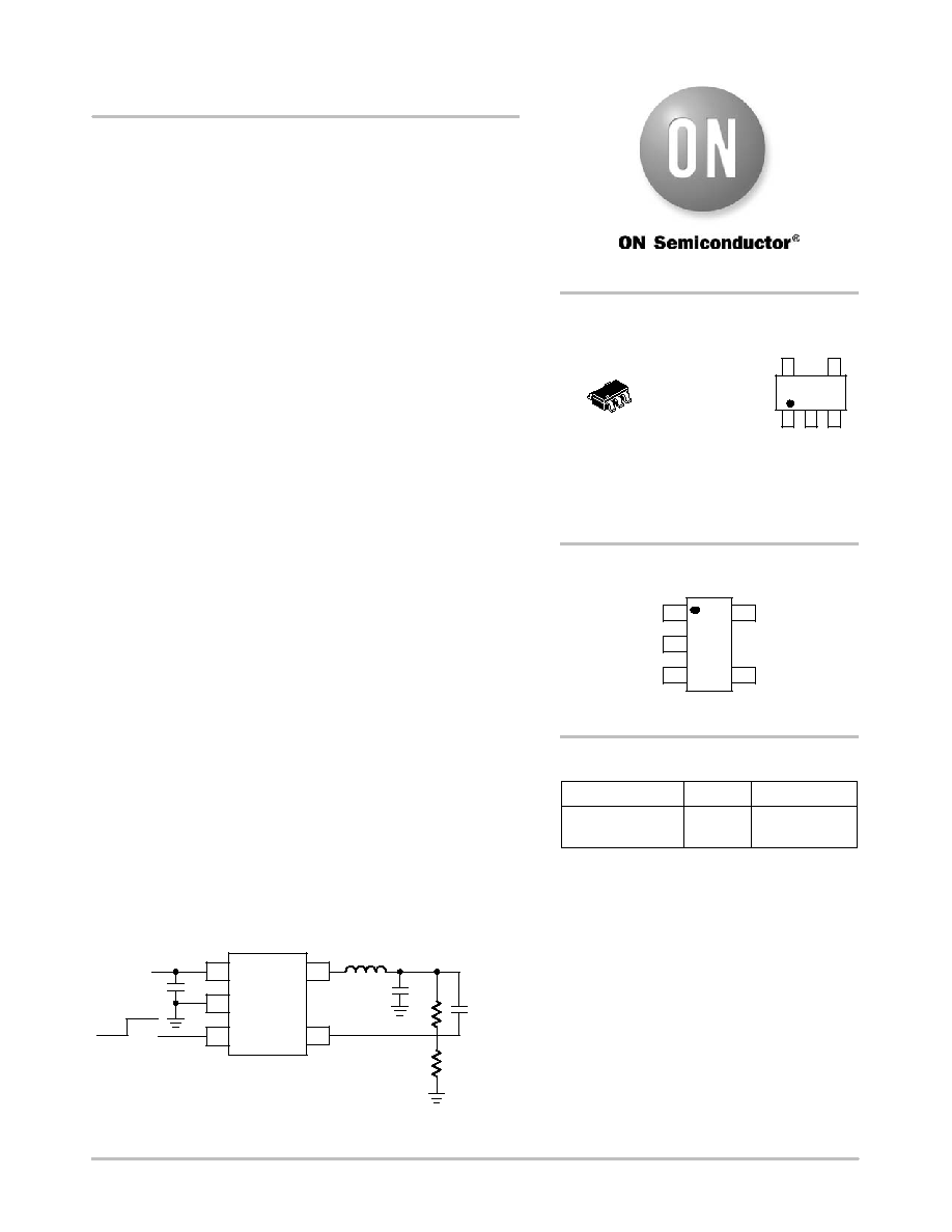
V
out
= 3.3 V
V
in
= 4.5 V
T
A
= 25
∞
C
100
90
80
70
60
50
500
600
400
300
200
100
0
I
out
(mA)
E
f
f (%)
Figure 2. Efficiency vs. Output Current
GND
2
VIN
1
Vbattery
4.7
m
F
EN
3
Enable
LOGIC
CONTROL
& THERMAL
SHUTDOWN
PWM/BURST
CONTROL
ILIMIT
REFERENCE
VOLTAGE
FB
4
LX
5
Q1
4.7
m
F
18 pF
R1
R2
2.2
m
H
Q2
Figure 3. Simplified Block Diagram

NCP1522
http://onsemi.com
3
PIN FUNCTION DESCRIPTION
Pin No.
Symbol
Function
Description
1
VIN
Analog Input
Power Supply Input for Analog V
CC
.
2
GND
Analog/Power Ground
Ground connection for the NFET Power Stage and the Analog Sections of the IC.
3
EN
Digital Input
Enable for Switching Regulator. This pin is active high. This pin contains an
internal pulldown resistor.
4
FB
Analog Input
Feedback voltage from the output of the power supply. This is the input to the
error amplifier.
5
LX
Analog Output
Connection from Power MOSFETs to the Inductor. For one option, an output
discharge circuit sinks current from this pin.
MAXIMUM RATINGS
Rating
Symbol
Value
Unit
Minimum Voltage All Pins
V
min
-0.3
V
Maximum Voltage All Pins (Note 2)
V
max
7.0
V
Maximum Voltage Enable, FB, LX
V
max
VIN + 0.3
V
Thermal Resistance, Junction -to-Air
R
q
JA
200
_
C/W
Operating Ambient Temperature Range
T
A
-40 to 85
_
C
Storage Temperature Range
T
stg
-55 to 150
_
C
Junction Operating Temperature
T
j
-40 to 125
_
C
Latch-up Current Maximum Rating (T
A
= 85
∞
C) (Note 4)
Lu
+/-100
mA
ESD Withstand Voltage (Note 3)
Human Body Model
Machine Model
Vesd
2.0
200
kV
V
Maximum ratings are those values beyond which device damage can occur. Maximum ratings applied to the device are individual stress limit values
(not normal operating conditions) and are not valid simultaneously. If these limits are exceeded, device functional operation is not implied, damage
may occur and reliability may be affected.
1. Maximum electrical ratings are defined as those values beyond which damage to the device may occur at T
A
= 25
∞
C.
2. According to JEDEC standard JESD22-A108B.
3. This device series contains ESD protection and exceeds the following tests:
Human Body Model (HBM) per JEDEC standard: JESD22-A114.
Machine Model (MM) per JEDEC standard: JESD22-A115.
4. Latchup current maximum rating per JEDEC standard: JESD78.
NCP1522
http://onsemi.com
4
ELECTRICAL CHARACTERISTICS
(Typical values are referenced to T
A
= +25
∞
C, Min and Max values are referenced -40
∞
C to
+85
∞
C ambient temperature, unless otherwise noted, operating conditions V
IN
= 3.6 V, V
OUT
= 1.8 V, unless otherwise noted.)
Characteristic
Symbol
Min
Typ
Max
Unit
Input Voltage Range
V
IN
2.7
-
5.5
V
Undervoltage Lockout (V
IN
Falling)
V
UVLO
2.3
2.5
2.6
V
Quiescent Current (PFM No Load)
I
q
-
60
95
m
A
Standby Current, EN Low
Istb
-
0.3
1.2
m
A
Oscillator Frequency
F
osc
2.400
3.0
3.600
MHz
Peak Inductor Current
I
LIM
-
1200
-
mA
Feedback Reference Voltage
V
ref
-
0.6
-
V
FB Pin Tolerance
VFBtol
-3.0
-
3.0
%
Reference Voltage Line Regulation
D
VFB
-
0.1
-
%
Output Voltage Accuracy (Note 5)
V
OUT
-3%
Vnom
+3%
V
Minimum Output Voltage
V
OUT
-
0.9
-
V
Maximum Output Voltage
V
OUT
-
3.3
-
V
Output Voltage Line Regulation (V
in
= 2.7≠5.5)
Io = 200 mA
D
V
OUT
-
0.1
-
%
Voltage Load Regulation
(IO = 200 mA to 300 mA)
(IO = 200 mA to 600 mA)
V
LOADREG
-
-
0.0005
0.001
-
-
%/mA
%/mA
Load Transient Response (300 mA to 600 mA Load Step, Trise 1.0
m
s)
V
OUT
-
35
-
mV
Duty Cycle
-
-
-
100
%
P-Ch On-Resistance
RLxH
-
300
-
m
W
N-Ch On-Resistance
RLxL
-
300
-
m
W
P-Ch Leakage Current
ILeakH
-
0.05
-
m
A
N-Ch Leakage Current
ILeakL
-
0.01
-
m
A
Enable Pin High
VENH
1.2
-
-
V
Enable Pin Low
VENL
-
-
0.4
V
EN << H >> Input Current, EN = 3.6 V
IENH
-
2.0
-
m
A
Soft-Start Time
T
start
-
350
500
m
s
Thermal Shutdown Threshold
T
SD
-
160
-
∞
C
Thermal Shutdown Hysteresis
T
SDH
-
25
-
∞
C
5. The overall output voltage tolerance depends upon the accuracy of the external resistor (R1, R2).
NCP1522
http://onsemi.com
5
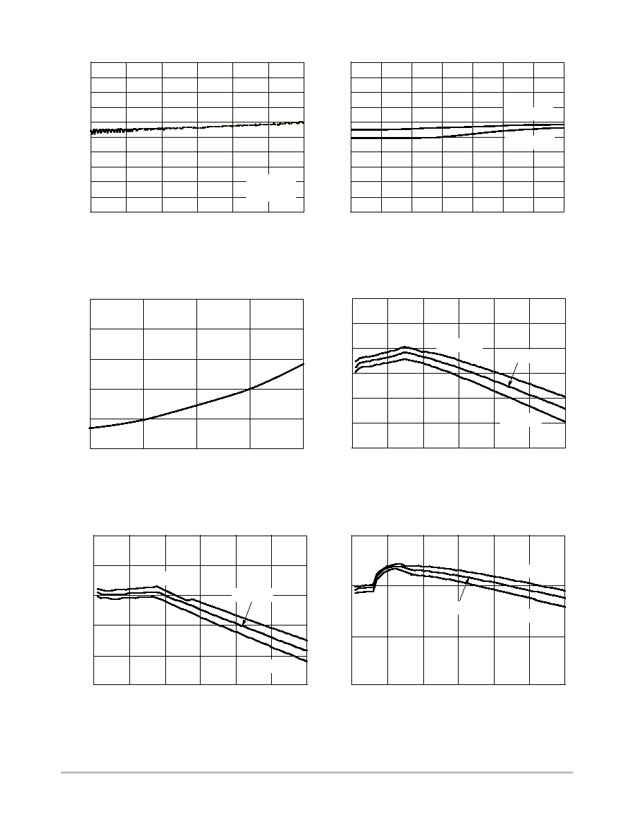
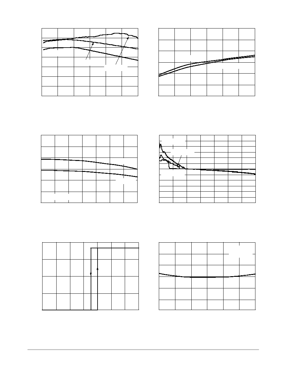
Figure 4. Quiescent Current vs. Supply Voltage
Figure 5. Quiescent Current vs. Temperature
Figure 6. Shutdown Current vs. Supply Voltage
Figure 7. Efficiency vs. Output Current
(V
OUT
= 1.8 V, V
IN
= 3.6 V)
Figure 8. Efficiency vs. Output Current
(V
OUT
= 0.9 V, V
IN
= 3.6 V)
Figure 9. Efficiency vs. Output Current
(V
OUT
= 3.3 V, V
IN
= 4.5 V)
0
I
OUT
, OUTPUT CURRENT (mA)
100
90
70
100
200
300
400
500
600
80
75
EFFICIENCY (%)
EFFICIENCY (%)
60
0
100
200
300
400
500
I
OUT
, OUTPUT CURRENT (mA)
50
QUIESCENT CURRENT (
m
A)
V
IN
, INPUT VOLTAGE (V)
0
10
20
30
40
50
2.7
3.2
3.7
4.2
4.7
SHUTDOWN CURRENT (
m
A)
2.7
3.2
4.7
1.0
0.6
0.4
0.2
0
V
IN
, INPUT VOLTAGE (V)
3.7
600
EN = V
IN
I
OUT
= 0 mA
5.2
5.7
T
A
= 25
∞
C
100
80
70
90
60
70
80
90
100
QUIESCENT CURRENT (
m
A)
TEMPERATURE (
∞
C)
0
10
20
30
40
50
-40
-20
0
20
40
V
IN
= 5.5 V
60
100
60
70
80
90
100
V
IN
= 2.7 V
80
0.8
4.2
EN = V
IN
I
OUT
= 0 mA
95
85
T
A
= 85
∞
C
T
A
= -40
∞
C
T
A
= 25
∞
C
T
A
= 85
∞
C
T
A
= -40
∞
C
EFFICIENCY (%)
0
100
200
300
400
500
I
OUT
, OUTPUT CURRENT (mA)
600
100
80
70
90
T
A
= 25
∞
C
T
A
= 85
∞
C
T
A
= -40
∞
C
NCP1522
http://onsemi.com
6
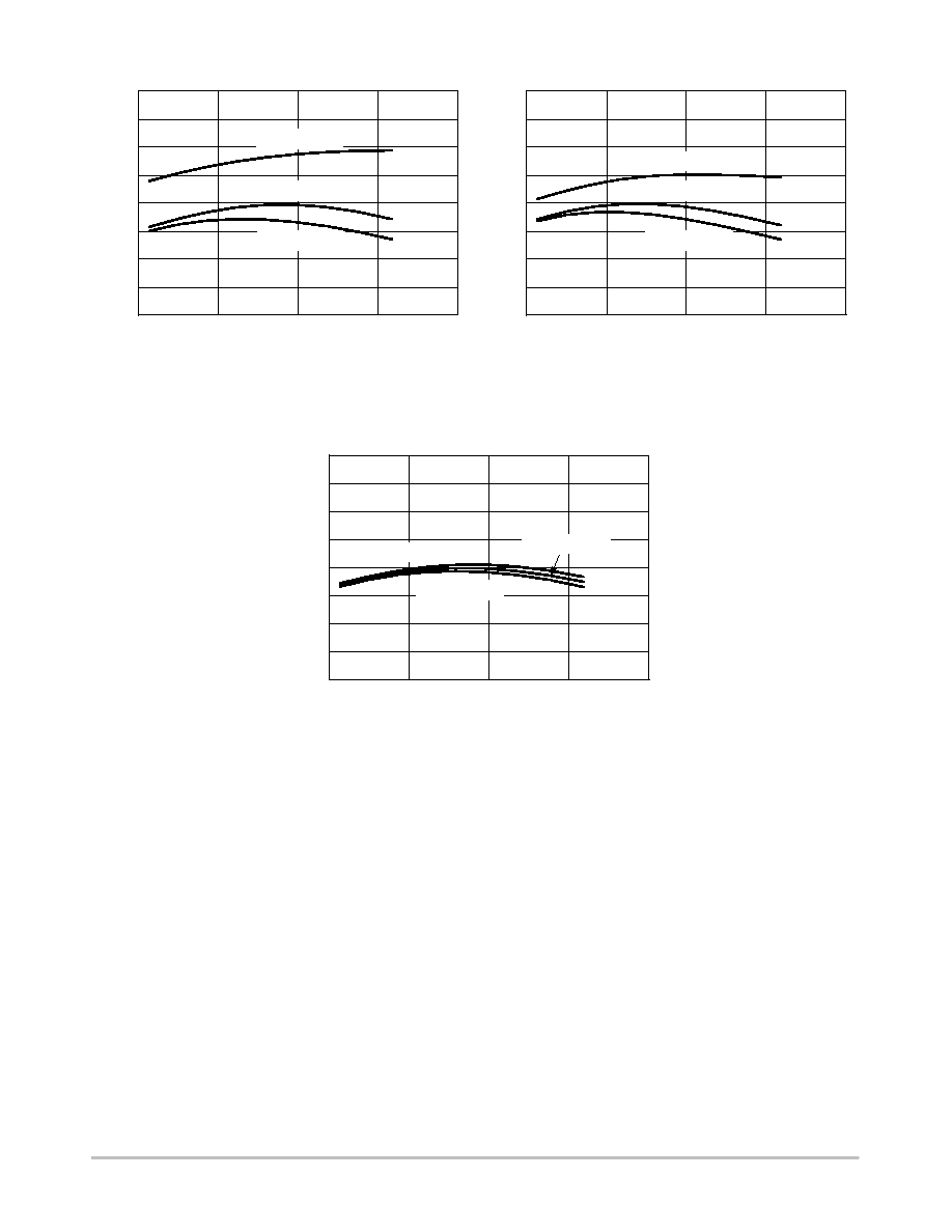
Figure 10. Efficiency vs. Output Current
(V
IN
= 4.0 V)
Figure 11. Frequency vs. Input Voltage
Figure 12. Frequency vs. Temperature
Figure 13. Load Regulation
Figure 14. Output Voltage vs. Enable Input Pin
Voltage
Figure 15. PFM/PWM Threshold vs. Input
Voltage
0
I
OUT
, OUTPUT CURRENT (mA)
3.0
1.0
-3.0
100
200
300
400
500
700
-1.0
-2.0
LOAD REGULA
TION (%)
OUTPUT VOL
T
AGE (V)
0.5
0
0.2
0.4
0.6
0.8
1.0
V
IN
, ENABLE INPUT VOLTAGE (V)
0.0
1.4
1.5
1.0
2.0
FREQUENCY (MHz)
V
IN
, INPUT VOLTAGE (V)
2.4
2.6
2.8
3.0
3.2
3.4
2.7
3.2
3.7
4.2
4.7
5.7
3.6
5.2
2.0
0.0
OUTPUT CURRENT (mA)
2.7
3.2
3.7
4.2
4.7
5.2
V
IN
, INPUT VOLTAGE (V)
5.7
300
100
0
200
0
I
OUT
, OUTPUT CURRENT (mA)
100
80
30
100
200
300
400
500
600
60
50
EFFICIENCY (%)
90
70
V
OUT
= 3.3 V
V
OUT
= 1.8 V
40
V
OUT
= 0.9 V
I
OUT
= 300 mA
I
OUT
= 600 mA
FREQUENCY (MHz)
TEMPERATURE (
∞
C)
2.4
2.6
2.8
3.0
3.2
3.4
-40
-20
0
20
40
100
3.6
60
V
IN
= 5.5 V
I
OUT
= 300 mA
80
V
IN
= 3.6 V
1.5
-2.5
-0.5
-1.5
2.5
0.5
600
V
OUT
= 3.3 V
V
OUT
= 1.8 V
V
OUT
= 0.9 V
1.2
250
50
150
V
OUT
= 1.8 V
T
A
= 25
∞
C
NCP1522
http://onsemi.com
7
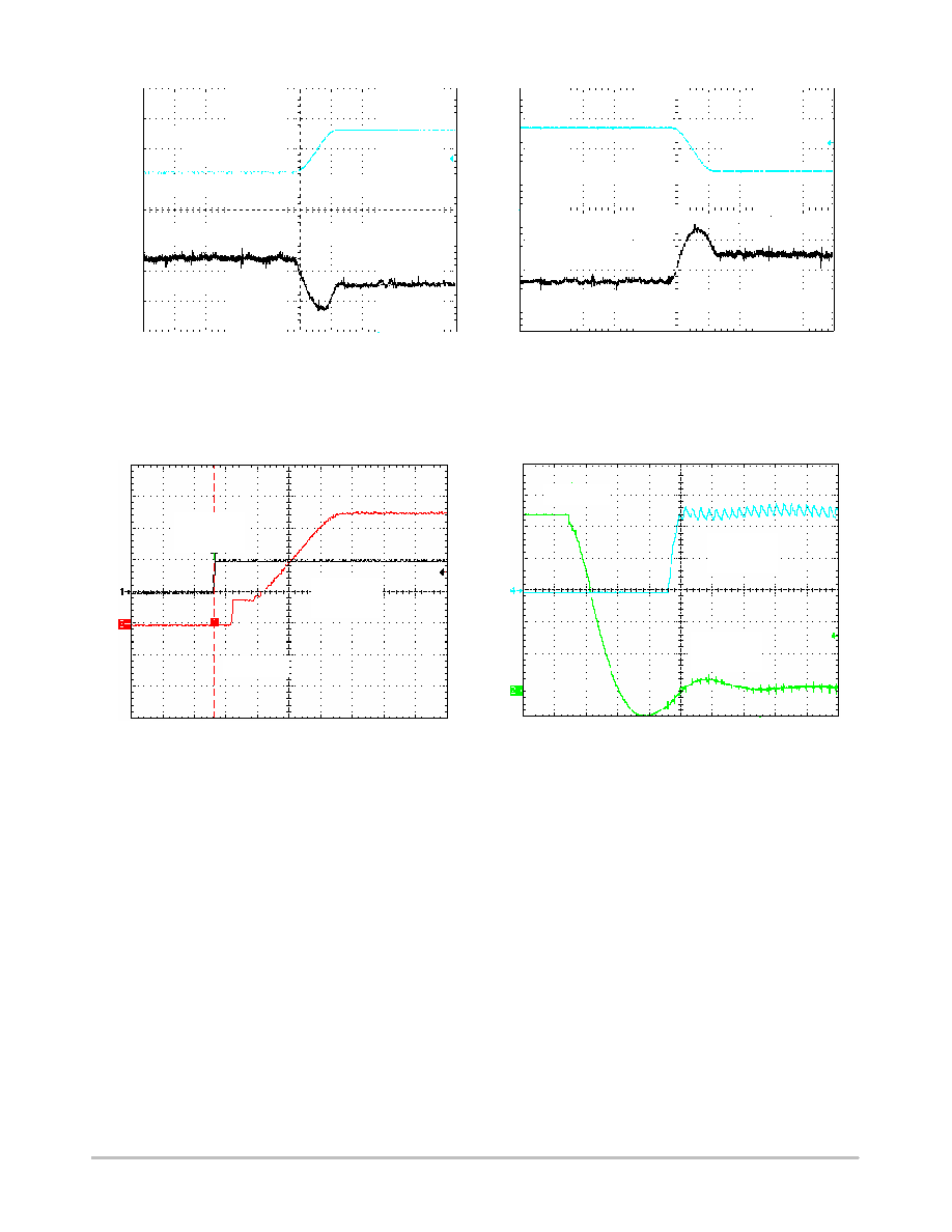
Figure 16. Output Voltage Accuracy
(V
OUT
= 0.9 V)
Figure 17. Output Voltage Accuracy
(V
OUT
= 1.8 V)
Figure 18. Output Voltage Accuracy
(V
OUT
= 3.3 V)
-50
TEMPERATURE (
∞
C)
1.0
0
50
100
150
-1.0
-2.0
OUTPUT VOL
T
AGE (%)
2.0
0.0
1.5
-0.5
-1.5
0.5
I
OUT
= 600 mA
I
OUT
= 300 mA
I
OUT
= 100 mA
-50
TEMPERATURE (
∞
C)
1.0
0
50
100
150
-1.0
-2.0
OUTPUT VOL
T
AGE (%)
2.0
0.0
1.5
-0.5
-1.5
0.5
I
OUT
= 600 mA
I
OUT
= 300 mA
I
OUT
= 100 mA
-50
TEMPERATURE (
∞
C)
1.0
0
50
100
150
-1.0
-2.0
OUTPUT VOL
T
AGE (%)
2.0
0.0
1.5
-0.5
-1.5
0.5
I
OUT
= 600 mA
I
OUT
= 300 mA
I
OUT
= 100 mA
V
IN
= 3.6 V
V
IN
= 3.6 V
V
IN
= 4.0 V
NCP1522
http://onsemi.com
8
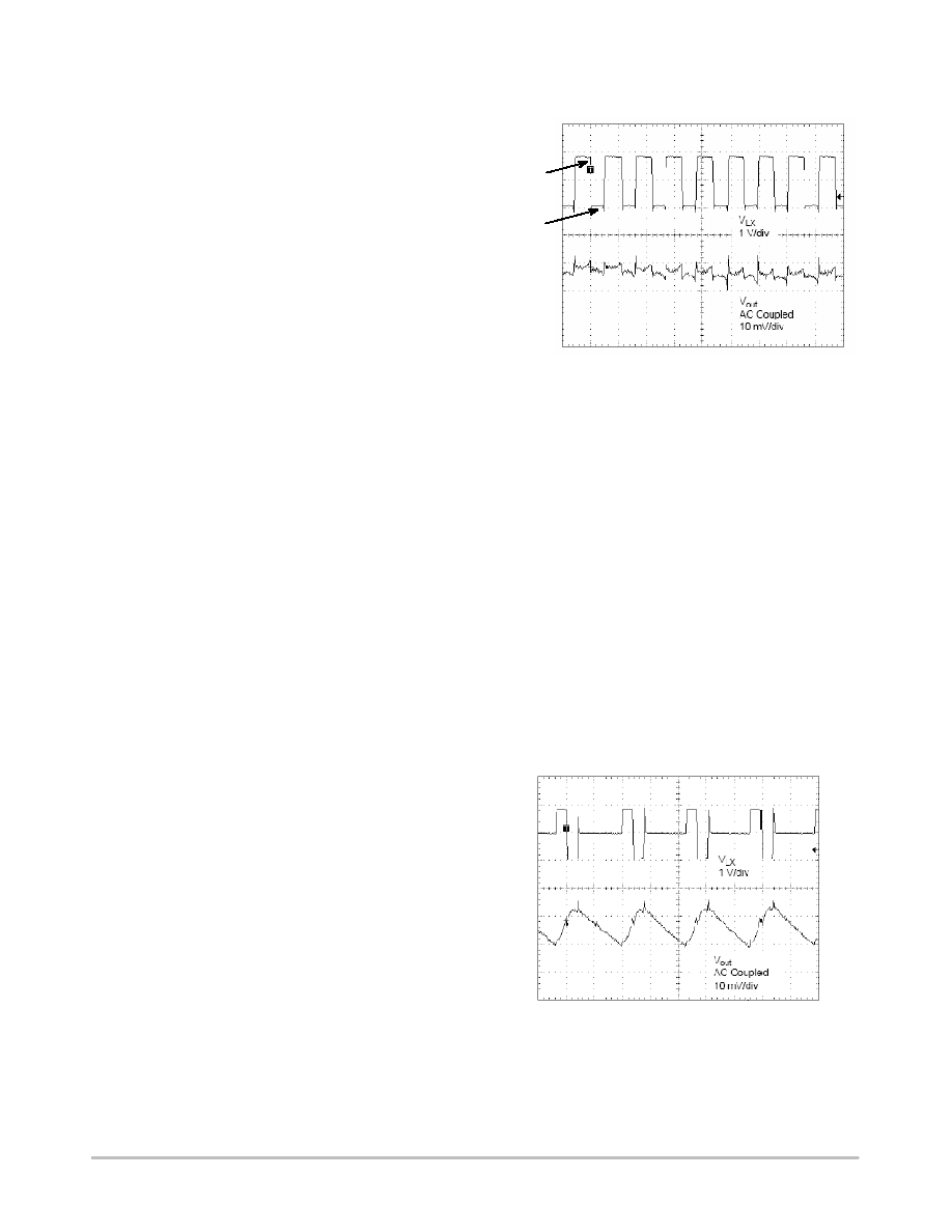
Figure 19. Load Transient Response in PWM
Operation (V
IN
= 3.6 V)
Figure 20. Load Transient Response in PWM
Operation (V
IN
= 3.6 V)
Figure 21. Soft Start Time (V
IN
= 3.6 V)
Figure 22. Short Circuit Protection (V
IN
= 3.6 V)
I
OUT
200 mA/Div
V
OUT
20 mV/Div
10
m
s/Div
I
OUT
200 mA/Div
V
OUT
20 mV/Div
10
m
s/Div
EN
2 V/Div
V
OUT
500 mV/Div
100
m
s/Div
V
OUT
500 mV/Div
2.5
m
s/Div
I
LX
500 mA/Div
NCP1522
http://onsemi.com
9
OPERATION DESCRIPTION
Overview
The NCP1522 uses a constant frequency, voltage mode
step-down architecture. Both the main (P-Channel
MOSFET) and synchronous (N-Channel MOSFET)
switches are internal.
It delivers a constant voltage from either a single Li-Ion
or three cell NiMH/NiCd battery to portable devices such
as cell phones and PDA. The output voltage is set by
external resistor divider. The NCP1522 sources at least
600 mA depending on external components chosen.
The NCP1522 works with two modes of operation; PWM
depending on the current required. The device operates in
PWM/PFM mode at load currents of approximately 80 mA
or higher, having voltage tolerance of
"3% with 90%
efficiency or better. Lighter load currents cause the device
to automatically switch into PFM mode for reduced current
consumption (IQ = 60
mA typ) and extended battery life.
Additional features include soft-start, undervoltage
protection, current overload protection, and thermal
shutdown protection. As shown in Figure 1, only six
external components are required for implementation. The
part uses an internal reference voltage of 0.6 V. It is
recommended to keep the part in shutdown until the input
voltage is 2.7 V or higher.
PWM Operating Mode
In this mode, the output voltage of the NCP1522 is
regulated by modulating the on-time pulse width of the
main switch Q1 at a fixed frequency of 3.0 MHz. The
switching of the PMOS Q1 is controlled by a flip-flop
driven by the internal oscillator and a comparator that
compares the error signal from an error amplifier with the
PWM ramp. At the beginning of each cycle, the main
switch Q1 is turned ON by the rising edge of the internal
oscillator clock. The inductor current ramps up until the
sum of the current sense signal and compensation ramp
becomes higher than the error voltage amplifier. Once this
has occurred, the PWM comparator resets the flip-flop, Q1
is turned OFF and the synchronous switch Q2 is turned ON.
Q2 replaces the external Schottky diode to reduce the
conduction loss and improve the efficiency. To avoid
overall power loss, a certain amount of dead time is
introduced to ensure Q1 is completely turned OFF before
Q2 is being turned ON.
Q1 ON
Q2 ON
1
m
s/div
Figure 23. PWM Switching Waveform
(V
in
= 3.6 V, V
out
= 1.8 V, I
out
= 300 mA)
PFM Operating Mode
Under light load conditions, the NCP1522 enters in low
current PFM mode operation to reduce power
consumption. The output regulation is implemented by
pulse frequency modulation. If the output voltage drops
below the threshold of PFM comparator (typically
Vnom-2%), a new cycle will be initiated by the PFM
comparator to turn on the switch Q1. Q1 remains ON until
the peak inductor current reaches 200 mA (nom). Then
ILIM comparator goes high to switch off Q1. After a short
dead time delay, switch rectifier Q2 is turned ON. The
negative current detector (NCD) will detect when the
inductor current drops below zero and sends the signal to
turn off Q2. The output voltage continues to decrease
through discharging the output capacitor. When the output
voltage falls below the threshold of the PFM comparator,
a new cycle starts immediately.
1
m
s/div
Figure 24. PFM Mode Switching Waveform
(V
in
= 3.6 V, V
out
= 1.8 V, I
out
= 30 mA)

NCP1522
http://onsemi.com
10
Cycle-by-Cycle Current Limitation
From the block diagram (Figure 3), an ILIM comparator
is used to realize cycle-by-cycle current limit protection.
The comparator compares the LX pin voltage with the
reference voltage, which is biased by a constant current. If
the inductor current reaches the limit, the ILIM comparator
detects the LX voltage falling below the reference voltage
and releases the signal to turn off the switch Q1. The
cycle-by-cycle current limit is set at 1200 mA (nom).
Short Circuit Protection
When the output is shorted to ground, the device limits
the inductor current. The duty-cycle is minimum and the
consumption on the input line is 300 mA (Typ). When the
short circuit condition is removed, the device returns to the
normal mode of operation.
Soft-Start
The NCP1522 uses soft-start (300
ms Typ) to limit the
inrush current when the device is initially powered up or
enabled. Soft-start is implemented by gradually increasing
the reference voltage until it reaches the full reference
voltage. During startup, a pulsed current source charges the
internal soft-start capacitor to provide gradually
increasing reference voltage. When the voltage across the
capacitor ramps up to the nominal reference voltage, the
pulsed current source will be switched off and the reference
voltage will switch to the regular reference voltage.
Shutdown Mode
When the EN pin has a voltage applied of less than 0.4 V,
the NCP1522 will be disabled. In shutdown mode, the
internal reference, oscillator and most of the control
circuitries are turned off. Therefore, the typical current
consumption will be 0.3
mA (typical value). Applying a
voltage above 1.2 V to EN pin will enable the device for
normal operation. The device will go through soft-start to
normal operation.
Thermal Shutdown
Internal Thermal Shutdown circuitry is provided to
protect the integrated circuit in the event that the maximum
junction temperature is exceeded. If the junction
temperature exceeds 160
_C, the device shuts down. In this
mode switch Q1 and Q2 and the control circuits are all
turned off. The device restarts in soft-start after the
temperature drops below 135
_C. This feature is provided
to prevent catastrophic failures from accidental device
overheating and it is not intended as a substitute for proper
heatsinking.
Low Dropout Operation
The NCP1522 offers a low input to output voltage
difference. The NCP1522 can operate at 100% duty cycle.
In this mode the PMOS (Q1) switches completely on.
The minimum input voltage to maintain regulation can
be calculated as:
VIN(min)
+
VOUT(max)
(eq. 1)
)
(IOUT
(RDS(on)
)
RINDUCTOR))
∑
V
OUT
: Output Voltage (Volts)
∑
I
OUT
: Max Output Current
∑
R
DS(on)
: P-Channel Switch R
DS(on)
∑
R
INDUCTOR
: Inductor Resistance (DCR)

NCP1522
http://onsemi.com
11
APPLICATION INFORMATION
Output Voltage Selection
The output voltage is programmed through an external
resistor divider connected from V
OUT
to FB then to GND.
For low power consumption and noise immunity, the
resistor from FB to GND (R2) should be in the
[100 k-600 k] range. If R2 is 200 k given the V
FB
is 0.6 V,
the current through the divider will be 3.0
mA.
The formula below gives the value of V
OUT
, given the
desired R1 and the R1 value:
VOUT
+
VFB
(1
)
R1
R2
)
(eq. 2)
∑
V
OUT
: Output Voltage (Volts)
∑
V
FB
: Feedback Voltage = 0.6 V
∑
R1: Feedback Resistor from V
OUT
to FB
∑
R2: Feedback Resistor from FB to GND
Input Capacitor Selection
In PWM operating mode, the input current is pulsating
with large switching noise. Using an input bypass capacitor
can reduce the peak current transients drawn from the
input supply source, thereby reducing switching noise
significantly. The capacitance needed for the input bypass
capacitor depends on the source impedance of the input
supply.
The maximum RMS current occurs at 50% duty cycle
with maximum output current, which is IO, max/2.
For NCP1522, a low profile, low ESR ceramic capacitor
of 4.7
mF should be used for most of the cases. For effective
bypass results, the input capacitor should be placed as close
as possible to the V
IN
pin.
Table 1. List of Input Capacitor
Murata
GRM188R60J475KE
GRM21BR71C475KA
Taiyo Yuden
JMK212BY475MG
TDK
C2012X5ROJ475KB
C1632X5ROJ475KT
Output L-C Filter Design Considerations
The NCP1522 is built in 3.0 MHz frequency and uses
voltage mode architecture. The correct selection of the
output filter ensures good stability and fast transient
response.
Due to the nature of the buck converter, the output L-C
filter must be selected to work with internal compensation.
For NCP1522, the internal compensation is internally fixed
and it is optimized for an output filter of L = 2.2
mH and
C
OUT
= 4.7
mF.
The corner frequency is given by:
fc
+
1
2
p
L
COUT
(eq. 3)
+
1
2
p
2.2
m
H
4.7
m
F
+
49.5 kHz
The device is intended to operate with inductance
between 1.0
mH and maximum of 4.7 mH.
If the corner frequency is moved, it is recommended to
check the loop stability depending on the output ripple
voltage accepted and output current required. For lower
frequency, the stability will be increased; a larger output
capacitor value could be chosen without critical effect on
the system. On the other hand, a smaller capacitor value
increases the corner frequency and it should be critical for
the system stability. Take care to check the loop stability.
The phase margin is usually higher than 45
∞.
Table 2. L-C Filter Example
Inductance (L)
Output Capacitor (C
out
)
1.0
m
H
10
m
F
2.2
m
H
4.7
m
F
4.7
m
H
2.2
m
F
Inductor Selection
The inductor parameters directly related to device
performances are saturation current and DC resistance and
inductance value. The inductor ripple current (ƒI
L
)
decreases with higher inductance:
D
IL
+
VOUT
L
fSW
1-
VOUT
VIN
(eq. 4)
DI
L
peak to peak inductor ripple current
L inductor value
f
SW
switching frequency
The saturation current of the inductor should be rated
higher than the maximum load current plus half the ripple
current:
D
IL(MAX)
+ D
IO(MAX)
) D
IL
2
(eq. 5)
DI
L(MAX)
Maximum inductor current
DI
O(MAX)
Maximum Output current
The inductor's resistance will factor into the overall
efficiency of the converter. For best performances, the DC
resistance should be less than 0.3
W for good efficiency.
NCP1522
http://onsemi.com
12
Table 3. List of Inductor
FDK
MIPW3226 Series
TDK
VLF3010AT Series
Taiyo Yuden
LQ CBL2012
Coil craft
DO1605-T Series
LPO3010
Output Capacitor Selection
Selecting the proper output capacitor is based on the
desired output ripple voltage. Ceramic capacitors with low
ESR values will have the lowest output ripple voltage and
are strongly recommended. The output capacitor requires
either an X7R or X5R dielectric.
The output ripple voltage in PWM mode is given by:
D
VOUT
+ D
IL
1
4
fSW-3
COUT
)
ESR
(eq. 6)
In PFM mode (at light load), the output voltage is
regulated by pulse frequency modulation. The output
voltage ripple is independent of the output capacitor value.
It is set by the threshold of PFM comparator.
Table 4. List of Output Capacitor
Murata
GRM188R60J475KE
4.7
m
F
GRM21BR60J106ME19L
10
m
F
GRM188R60OJ106ME
10
m
F
Taiyo Yuden
JMK212BY475MG
4.7
m
F
JMK212BJ106MG
10
m
F
TDK
C2012X5ROJ475KB
4.7
m
F
C1632X5ROJ475KT
4.7
m
F
C2012X5ROJ106K
10
m
F
Feed-Forward Capacitor Selection
The feed-forward capacitor sets the feedback loop
response and is critical to obtain good loop stability.
Given that the compensation is internally fixed, an 18 pF
or higher ceramic capacitor is needed. Choose a small
ceramic capacitor X7R or X5R or COG dielectric.
NCP1522
http://onsemi.com
13
APPLICATION BOARD
PCB Layout Recommendations
Good PCB layout plays an important role in switching
mode power conversion. Careful PCB layout can help to
minimize ground bounce, EMI noise and unwanted
feedback that can affect the performance of the converter.
Hints suggested below can be used as a guideline in most
situations.
1. Use star-ground connection to connect the IC
ground nodes and capacitor GND nodes together
at one point. Keep them as close as possible, and
then connect this to the ground plane through
several vias. This will reduce noise in the ground
plane by preventing the switching currents from
flowing through the ground plane.
2. Place the power components (i.e., input capacitor,
inductor and output capacitor) as close together
as possible for best performance. All connecting
traces must be short, direct, and wide to reduce
voltage errors caused by resistive losses through
the traces.
3. Separate the feedback path of the output voltage
from the power path. Keep this path close to the
NCP1522 circuit. And also route it away from
noisy components. This will prevent noise from
coupling into the voltage feedback trace.
4. Place the DC-DC converter away from noise
sensitive circuitry, such as RF circuits.
The following shows the NCP1522 demo board
schematic, layout, and bill of materials:
GND
2
VIN
1
EN
3
LX
5
FB
4
OFF ON
VIN
CIN
COUT
R1
R2
Cff
L
VOUT
Figure 25. NCP1522 Board Schematic
Figure 26. NCP1522 Board Layout
NCP1522
http://onsemi.com
14
J1
1
2
0
Power
C1
4.7
m
F
VIN
VFVIN
0
1
2
3
EN
U1
VP
GND
EN
FB
LX
5
4
LX
1
NCP152x
0
2
C2
4.7
m
F
R1
220 R
R2
220 R
0
C3
18 pF
VOUT
0
1
2
OUTPUT
J3
VP
1
2
3
CON3
J5
R3
220 K
0
EN
0
BNCH
J4
Figure 27. Schematics
2.2
m
H
L1
Figure 28. Silkscreen Layer
NCP1522
http://onsemi.com
15
Figure 29. Board Layout (Top View)
Figure 30. Board Layout (Bottom View)

NCP1522
http://onsemi.com
16
Bill of Materials
Item
Part Description
Ref
PCB Footprint
Manufacturer
Manufacturer
Reference
1
NCP1522 DC-DC Converter
U1
TSOP-5
On Semiconductor
NCP1522
2
4.7
m
F Ceramic Capacitor
6.3 V X5R
C1, C2
0805
Murata
GRM21 Series
3
18 pF Ceramic Capacitor
50 V COG
C3
0603
Murata
GRM188 Series
4
SMD Resistor 220 K
R1, R2, R3
0805
Vishay-Draloric
CRCW0805
5
SMD Inductor
L1
1605
Coilcraft
DO1605 Series
6
I/O Connector can be plugged by
BLZ5.08/2 (Weidm¸ller reference)
J1, J3
-
Weidm¸ller
SL5.08/2/90B
7
Jumper Header vertical mount 3*1,
2.54 mm
J5
-
Tyco Electronics/AMP
5-826629-0
8
Jumper Connector, 400 mils
J6, J7
-
Harwin
D3082-B01
NCP1522
http://onsemi.com
17
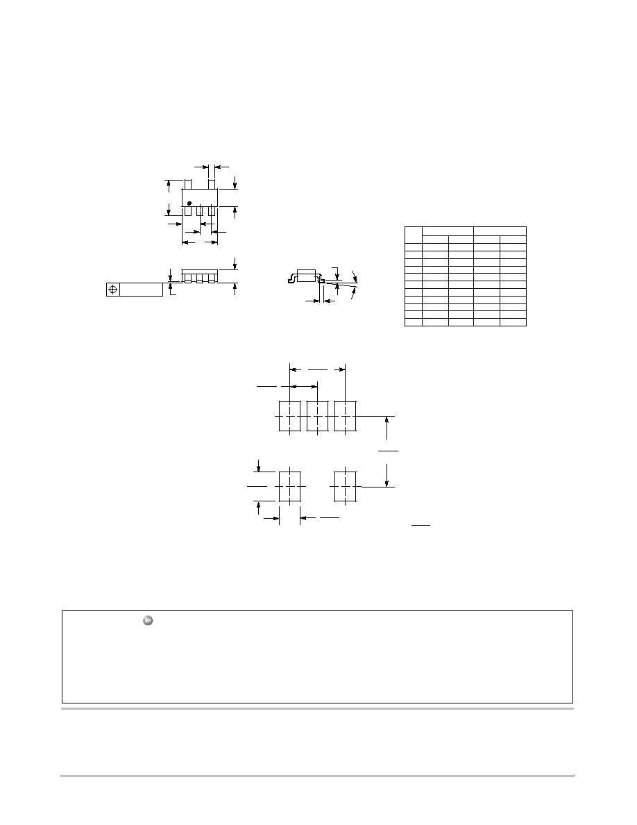
PACKAGE DIMENSIONS
TSOP-5
SN SUFFIX
CASE 483-02
ISSUE E
NOTES:
1. DIMENSIONING AND TOLERANCING PER
ANSI Y14.5M, 1982.
2. CONTROLLING DIMENSION: MILLIMETER.
3. MAXIMUM LEAD THICKNESS INCLUDES
LEAD FINISH THICKNESS. MINIMUM LEAD
THICKNESS IS THE MINIMUM THICKNESS
OF BASE MATERIAL.
4. A AND B DIMENSIONS DO NOT INCLUDE
MOLD FLASH, PROTRUSIONS, OR GATE
BURRS.
DIM
MIN
MAX
MIN
MAX
INCHES
MILLIMETERS
A
2.90
3.10
0.1142
0.1220
B
1.30
1.70
0.0512
0.0669
C
0.90
1.10
0.0354
0.0433
D
0.25
0.50
0.0098
0.0197
G
0.85
1.05
0.0335
0.0413
H
0.013
0.100
0.0005
0.0040
J
0.10
0.26
0.0040
0.0102
K
0.20
0.60
0.0079
0.0236
L
1.25
1.55
0.0493
0.0610
M
0
10
0
10
S
2.50
3.00
0.0985
0.1181
0.05 (0.002)
1
2
3
5
4
S
A
G
L
B
D
H
C
K
M
J
_
_
_
_
0.7
0.028
1.0
0.039
mm
inches
SCALE 10:1
0.95
0.037
2.4
0.094
1.9
0.074
*For additional information on our Pb-Free strategy and soldering
details, please download the ON Semiconductor Soldering and
Mounting Techniques Reference Manual, SOLDERRM/D.
SOLDERING FOOTPRINT*
ON Semiconductor and are registered trademarks of Semiconductor Components Industries, LLC (SCILLC). SCILLC reserves the right to make changes without further notice
to any products herein. SCILLC makes no warranty, representation or guarantee regarding the suitability of its products for any particular purpose, nor does SCILLC assume any
liability arising out of the application or use of any product or circuit, and specifically disclaims any and all liability, including without limitation special, consequential or incidental
damages. "Typical" parameters which may be provided in SCILLC data sheets and/or specifications can and do vary in different applications and actual performance may vary over
time. All operating parameters, including "Typicals" must be validated for each customer application by customer's technical experts. SCILLC does not convey any license under
its patent rights nor the rights of others. SCILLC products are not designed, intended, or authorized for use as components in systems intended for surgical implant into the body,
or other applications intended to support or sustain life, or for any other application in which the failure of the SCILLC product could create a situation where personal injury or death
may occur. Should Buyer purchase or use SCILLC products for any such unintended or unauthorized application, Buyer shall indemnify and hold SCILLC and its officers, employees,
subsidiaries, affiliates, and distributors harmless against all claims, costs, damages, and expenses, and reasonable attorney fees arising out of, directly or indirectly, any claim of
personal injury or death associated with such unintended or unauthorized use, even if such claim alleges that SCILLC was negligent regarding the design or manufacture of the part.
SCILLC is an Equal Opportunity/Affirmative Action Employer. This literature is subject to all applicable copyright laws and is not for resale in any manner.
PUBLICATION ORDERING INFORMATION
N. American Technical Support: 800-282-9855 Toll Free
USA/Canada
Japan: ON Semiconductor, Japan Customer Focus Center
2-9-1 Kamimeguro, Meguro-ku, Tokyo, Japan 153-0051
Phone: 81-3-5773-3850
NCP1522/D
LITERATURE FULFILLMENT:
Literature Distribution Center for ON Semiconductor
P.O. Box 61312, Phoenix, Arizona 85082-1312 USA
Phone: 480-829-7710 or 800-344-3860 Toll Free USA/Canada
Fax: 480-829-7709 or 800-344-3867 Toll Free USA/Canada
Email: orderlit@onsemi.com
ON Semiconductor Website: http://onsemi.com
Order Literature: http://www.onsemi.com/litorder
For additional information, please contact your
local Sales Representative.