©
Semiconductor Components Industries, LLC, 2004
November, 2004 - Rev. 3
1
Publication Order Number:
NCP1530/D
NCP1530
600 mA PWM/PFM
Step-Down Converter with
External Synchronization Pin
The NCP1530 is a PWM/PFM non-synchronous step-down
(Buck) DC-DC converter for usage in systems supplied from 1-cell
Li-ion, or 2 or more cells Alkaline/NiCd/NiMH batteries. It can
operate in Constant-Frequency PWM mode or PWM/PFM mode in
which the controller will automatically switch to PFM mode
operation at low output loads to maintain high efficiency. The
switching frequency can also be synchronized to external clock
between 600 kHz and 1.2 MHz. The maximum output current is up
to 600 mA. Applying an external synchronizing signal to SYN pin
can supersede the PFM operation.
The NCP1530 consumes only 47
mA (typ) of supply current
(V
OUT
= 3.0 V, no switching) and can be forced to shutdown mode by
bringing the enable input (EN) low. In shutdown mode, the regulator
is disabled and the shutdown supply current is reduced to
0.5
mA (typ). Other features include built-in undervoltage lockout,
internal thermal shutdown, an externally programmable soft-start
time and output current limit protection. The NCP1530 operates
from a maximum input voltage of 5.0 V and is available in a space
saving, low profile Micro8
TM
package.
Features
∑
Pb-Free Package is Available
∑
High Conversion Efficiency, up to 92% at V
IN
= 4.3 V,
V
OUT
= 3.3 V, I
OUT
= 300 mA
∑
Current-Mode PWM Control
∑
Automatic PWM/PFM Mode for Current Saving at Low Output Loads
∑
Internal Switching Transistor Support 600 mA Output Current
(V
IN
= 5.0 V, V
OUT
= 3.3 V)
∑
High Switching Frequency (600 kHz), Support Small Size Inductor
and Capacitor, Ceramic Capacitors Can be Used
∑
Synchronize to External Clock Signal up to 1.2 MHz
∑
100% Duty Cycle for Maximum Utilization of the Supply Source
∑
Programmable Soft-Start Time through External Chip Capacitor
∑
Externally Accessible Voltage Reference
∑
Built-In Input Undervoltage Lockout
∑
Built-In Output Overvoltage Protection
∑
Power Saving Shutdown Mode
∑
Space Saving, Low Profile Micro8 Package
Typical Applications
∑
PDAs
∑
Digital Still Camera
∑
Cellular Phone and Radios
∑
Portable Test Equipment
∑
Portable Scanners
∑
Portable Audio Systems
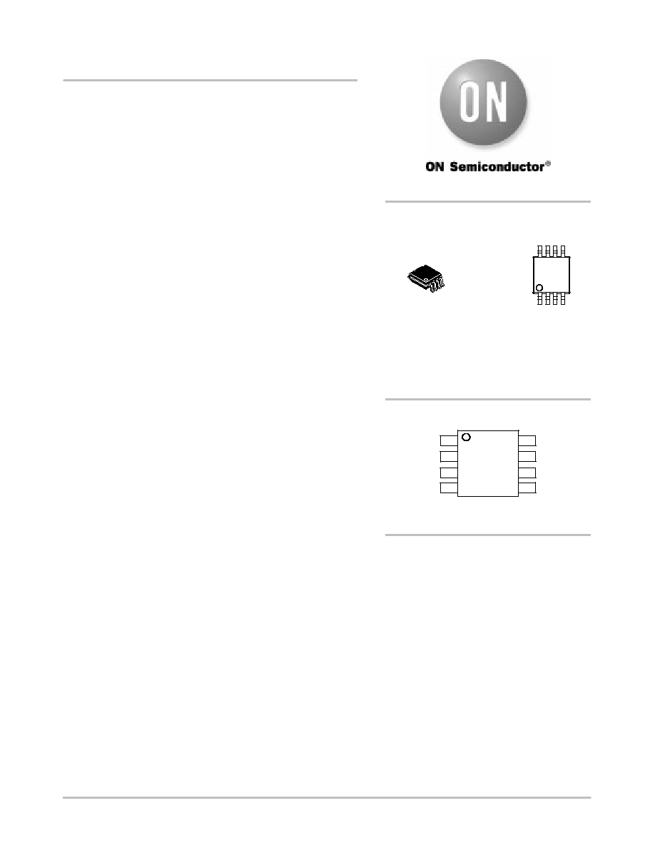
Micro8
]
DM SUFFIX
CASE 846A
1
8
PIN CONNECTIONS
http://onsemi.com
xxxx = Specific Device Code
A
= Assembly Location
L
= Wafer Lot
Y
= Year
W
= Work Week
MARKING
DIAGRAM
xxxx
ALYW
8
7
6
5
1
2
3
4
V
IN
SYN
SS
GND
LX
V
REF
V
OUT
EN
(Top View)
See detailed ordering and shipping information in the package
dimensions section on page 14 of this data sheet.
ORDERING INFORMATION

NCP1530
http://onsemi.com
2
Figure 1. Typical Step-Down Converter Application
V
IN
SYN
SS
GND
V
IN
= 2.8 V to 5.0 V
*C
SS
C
IN
22
m
F
NCP1530
LX
V
OUT
V
REF
EN
D1
MBRM120ET3
C
OUT
22
m
F
*C
VREF
1.0
m
F
L1
5.6
m
H
V
OUT
= 3.0 V
*Optional Component
Figure 2. Simplified Functional Block Diagram
ENABLE
DETECT
UVLO
EN 5
SYNC
DETECT
AND
TIMING
BLOCK
SYN 2
MODE
SELECTION
MASTER ENABLE
MODE
DRV
CONTROL
LOGIC
OV
-
+
-
+
-
+
OTA
-
+
FB
SS 3
4 GND
ISEN
V
IN
1
6 V
OUT
8 LX
THERMAL
SHUTDOWN
50 nA
ISEN
+
-
0.04
V
REF
VOLTAGE
REFERENCE
AND
SOFT-START
10 pF
V
REF
7
V
REF
ILIMIT
ISEN
ISEN
FB

NCP1530
http://onsemi.com
3
PIN FUNCTION DESCRIPTIONS
Pin
Symbol
Description
1
V
IN
Unregulated Supply Input.
2
SYN
Oscillator Synchronization and Mode Selection Input.
SYNC = GND (Automatic PWM/PFM mode) The converter operates at 600 kHz fixed-frequency PWM mode
primarily, and automatically switches to variable-frequency PFM mode at small output loads for power saving.
SYNC = V
IN
(Constant-Frequency PWM mode) The converter operates at 600 kHz fixed-frequency PWM mode
always.
SYNC = External clock signal between 600 to 1200 kHz. The converter will be synchronized with the external
clock signal.
The SYNC pin is internally pulled to GND.
3
SS
Soft-Start Timing control pin. An external soft-start capacitor can be connected to this pin if extended soft-start is
required. A 50 nA current will be sourced from this pin to charge up the capacitor during startup and gently ramps
the device into service to prevent output voltage overshoot. If this pin is floated, built-in 500
m
s (typ.)
soft-start
will be activated.
4
GND
Ground Terminal.
5
EN
Active-High Enable Input. Active to enable the device. Bring this pin to GND and the quiescent current is reduced
to less than 0.5
m
A. This pin is internally pulled to V
IN
.
6
V
OUT
Feedback Terminal. The output voltage is sensed by this pin.
7
V
REF
Connected to voltage reference decoupling capacitor. For noise non-sensitive applications, the internal voltage
reference can operate without decoupling capacitor.
8
LX
Inductor Terminal. This pin is connected to the drains of the internal P-channel switching transistors. The inductor
must be connected between this pin and the output terminal.
MAXIMUM RATINGS
Rating
Symbol
Value
Unit
Power Supply (Pin 1)
V
IN
-0.3 to 6
V
Input/Output Pins (Pins 2-4 & Pins 7-8)
V
IO
-0.3 to 6
V
Thermal Characteristics
Micro8 Plastic Package
Thermal Resistance, Junction-to-Air
R
q
JA
240
∞
C/W
Operating Junction Temperature Range
T
J
0 to +150
∞
C
Operating Ambient Temperature Range
T
A
0 to +85
∞
C
Storage Temperature Range
T
stg
-55 to +150
∞
C
Maximum ratings are those values beyond which device damage can occur. Maximum ratings applied to the device are individual stress limit values
(not normal operating conditions) and are not valid simultaneously. If these limits are exceeded, device functional operation is not implied, damage
may occur and reliability may be affected.
1. This device series contains ESD protection and exceeds the following tests:
Human Body Model (HBM)
"
2.0 kV per JEDEC standard: JESD22-A114.
Machine Model (MM)
"
200 V per JEDEC standard: JESD22-A115.
2. Latchup Current Maximum Rating:
"
150 mA per JEDEC standard: JESD78.
3. Moisture Sensitivity Level (MSL): 1 per IPC/JEDEC standard: J-STD-020A.

NCP1530
http://onsemi.com
4
ELECTRICAL CHARACTERISTICS
(V
IN
= V
R
+ 1.0 V, test circuit, refer to Figure 1, C
SS
= NC and C
VREF
= 1.0
m
F, T
A
= 25
∞
C for
typical value, 0
∞
C
T
A
85
∞
C for min/max values unless otherwise noted.) *V
R
is the factory-programmed output voltage setting.
Characteristic
Symbol
Min
Typ
Max
Unit
Input Voltage
V
IN
1.1 V
R
-
5.0
V
Output Voltage (I
load
= 150 mA, V
R
+ 1.0 V < V
IN
< 5.0 V) (Note 4)
NCP1530DM25R2
NCP1530DM27R2
NCP1530DM30R2
NCP1530DM33R2
V
OUT
2.425
2.619
2.910
3.201
2.5
2.7
3.0
3.3
2.575
2.781
3.090
3.399
V
Maximum Output Current (V
IN
= 5.0 V, V
OUT
= 3.0 V) (Note 5)
I
OUT(max)
600
-
-
mA
Supply Current (V
IN
= V
R
+ 1.0 V, No Load, EN and SYN Pins NC)
I
IN
-
45
95
m
A
Shutdown Supply Current (V
IN
= 5.0 V, No Load, V
EN
= 0 V)
I
SHDN
-
0.5
1.0
m
A
LX Pin Leakage Current (No Load, V
EN
= 0 V)
I
LX
-
-
1.0
m
A
Internal P-FET ON Resistance at LX Pin
(V
IN
= V
R
+ 1.0 V, I
Load
= 150 mA)
R
DS(ON)
-
0.3
0.5
W
Oscillator Frequency
(V
IN
= V
EN
= V
R
+ 1.0 V, I
Load
= 100 mA, SYN Pin NC)
f
OSC
480
600
720
kHz
Maximum PWM Duty Cycle (Note 5)
D
MAX-PWM
-
-
100
%
PFM to PWM Switch-Over Current Threshold
(V
IN
= 4.5 V, SYN Pin NC, L = 5.6
m
H, C
OUT
= 22
m
F) (Note 5)
NCP1530DM25R2
NCP1530DM27R2
NCP1530DM30R2
NCP1530DM33R2
I
PFM-PWM
-
-
-
-
83
90
100
102
-
-
-
-
mA
PWM to PFM Switch-Over Current Threshold
(V
IN
= 4.5 V, SYN Pin NC, L = 5.6
m
H, C
OUT
= 22
m
F) (Note 5)
NCP1530DM25R2
NCP1530DM27R2
NCP1530DM30R2
NCP1530DM33R2
I
PWM-PFM
-
-
-
-
27
38
39
48
-
-
-
-
mA
Input Undervoltage Lockout Threshold
V
UVLO
-
2.0
2.45
V
Reference Voltage (V
IN
= V
R
+ 1.0 V, C
VREF
= 1.0
m
F)
V
REF
1.184
1.20
1.216
V
Reference Voltage Temperature Coefficient
(V
IN
= V
R
+ 1.0 V, C
VREF
= 1.0
m
F) (Note 5)
TC
VREF
-
0.03
-
mV/
∞
C
Reference Voltage Load Current
(V
IN
= V
R
+ 1.0 V, C
VREF
= 1.0
m
F) (Note 6)
I
VREF
5.0
-
-
mA
Enable Logic High Threshold Voltage (V
IN
= V
R
+ 1.0 V, I
Load
= 0 mA)
V
EN-H
-
1.5
1.85
V
Enable Logic Low Threshold Voltage (V
IN
= V
R
+ 1.0 V, I
Load
= 0 mA)
V
EN-L
0.5
1.2
-
V
PWM Minimum On-Time (Note 5)
t
PWM-ON
-
100
-
ns
PWM OV Protection Level
%V
OV
-
6.0
12
%
PWM Cycle-by-Cycle Current Limit (Note 5)
I
LIM
-
1.5
-
A
Built-in Soft-Start Time (V
OUT
= 3.0 V, SS Pin NC) (Note 5)
t
SS
-
500
-
m
s
Thermal Shutdown Threshold (V
IN
= 3.5 V, I
Load
= 0 mA) (Note 5)
TH
SHD
-
145
-
∞
C
Thermal Shutdown Hysteresis (V
IN
= 3.5 V, I
Load
= 0 mA) (Note 5)
TH
HSYS
-
15
-
∞
C
4. Tested at V
IN
= V
R
+ 1.0 V in production only. Full V
IN
range guaranteed by design.
5. Parameter guaranteed by design only, not tested in production.
6. Loading capability decreases with V
OUT
decreases.

NCP1530
http://onsemi.com
5
TYPICAL OPERATING CHARACTERISTICS
(V
IN
= V
R
+ 1.0 V, test circuit, refer to Figure 1, C
SS
= NC and C
VREF
= 1.0
m
F, T
A
=
25
∞
C for typical value, 0
∞
C
T
A
85
∞
C for min/max values unless otherwise noted.) *V
R
is the factory-programmed output voltage setting.
3.3 V
I
S
HDN
, SHUTDOWN CURRENT (nA)
0
17
34
51
68
85
T
A
, AMBIENT TEMPERATURE (
∞
C)
Figure 3. Output Voltage vs. Ambient Temperature
(V
OUT
= 2.5 V)
2.40
2.45
2.50
2.55
2.60
0
17
34
51
68
85
T
A
, AMBIENT TEMPERATURE (
∞
C)
V
OU
T
, OUTPUT VOL
T
AGE (V)
Figure 4. Output Voltage vs. Ambient Temperature
(V
OUT
= 2.7 V)
2.90
2.95
3.00
3.05
3.10
Figure 5. Output Voltage vs. Ambient Temperature
(V
OUT
= 3.0 V)
Figure 6. Output Voltage vs. Ambient Temperature
(V
OUT
= 3.3 V)
3.20
3.25
3.30
3.35
3.40
30
45
60
75
90
Figure 7. Supply Current vs. Ambient Temperature
I
IN
, SUPPL
Y CURRENT (
m
A)
0
100
200
300
400
500
Figure 8. Shutdown Current vs. Ambient Temperature
2.60
2.65
2.70
2.75
2.80
0
17
34
51
68
85
T
A
, AMBIENT TEMPERATURE (
∞
C)
V
OU
T
, OUTPUT VOL
T
AGE (V)
0
17
34
51
68
85
T
A
, AMBIENT TEMPERATURE (
∞
C)
V
OU
T
, OUTPUT VOL
T
AGE (V)
0
17
34
51
68
85
T
A
, AMBIENT TEMPERATURE (
∞
C)
V
OU
T
, OUTPUT VOL
T
AGE (V)
I
Load
= 150 mA
V
IN
= 3.5 V
V
IN
= 5.0 V
I
Load
= 150 mA
V
IN
= 3.7 V
V
IN
= 5.0 V
I
Load
= 150 mA
V
IN
= 4.3 V
V
IN
= 5.0 V
I
Load
= 150 mA
V
IN
= 4.0 V
V
IN
= 5.0 V
0
17
34
51
68
85
T
A
, AMBIENT TEMPERATURE (
∞
C)
V
IN
= V
R
+ 1.0 V
I
Load
= 0 mA
3.0 V
3.0 V
3.3 V
2.7 V
2.5 V
V
IN
= 5.0 V
I
Load
= 0 mA
2.5 V

NCP1530
http://onsemi.com
6
0
20
40
60
80
100
120
140
4.25
4.5
4.75
I
LOAD
, OUTPUT LOADING CURRENT (mA)
V
IN
, INPUT VOLTAGE (V)
L = 5.6
m
H, C
OUT
= 22
m
F
SYN Pin = NC
PWM
PFM
5.0
0
20
40
60
80
100
120
140
3.5
4.0
4.5
5.0
I
LOAD
, OUTPUT LOADING CURRENT (mA)
V
IN
, INPUT VOLTAGE (V)
0
17
34
51
68
85
T
A
, AMBIENT TEMPERATURE (
∞
C)
3.0 V
3.3 V
2.7 V
2.5 V
450
525
600
675
750
Figure 9. Oscillator Frequency
vs. Ambient Temperature
f
OSC
,
OSCILLA
T
OR FREQUENCY (kHz)
0.10
0.20
0.30
0.40
0.50
R
DS
(
O
N)
, P-FET ON RESIST
ANCE (
W
)
Figure 10. P-FET ON Resistance
vs. Ambient Temperature
Figure 11. PWM/PFM Switchover Current
Thresholds vs. Input Voltage (V
OUT
= 2.5 V)
0
20
40
60
80
100
120
140
3.5
4.0
4.5
5.0
I
LOAD
, OUTPUT LOADING CURRENT (mA)
Figure 12. PWM/PFM Switchover Current
Thresholds vs. Input Voltage (V
OUT
= 2.7 V)
V
IN
, INPUT VOLTAGE (V)
Figure 13. PWM/PFM Switchover Current
Thresholds vs. Input Voltage (V
OUT
= 3.0 V)
Figure 14. PWM/PFM Switchover Current
Thresholds vs. Input Voltage (V
OUT
= 3.3 V)
0
17
34
51
68
85
T
A
, AMBIENT TEMPERATURE (
∞
C)
V
IN
= V
REN
=V
R
+ 1.0 V
I
Load
= 0 mA
SYN Pin = NC
3.0 V
3.3 V
2.7 V
2.5 V
V
IN
= V
REN
=V
R
+ 1.0 V
I
Load
= 0 mA
SYN Pin = NC
L = 5.6
m
H, C
OUT
= 22
m
F
SYN Pin = NC
PWM
PFM
L = 5.6
m
H, C
OUT
= 22
m
F
SYN Pin = NC
PWM
PFM
0
20
40
60
80
100
120
140
4.0
4.25
4.5
4.75
I
LOAD
, OUTPUT LOADING CURRENT (mA)
V
IN
, INPUT VOLTAGE (V)
L = 5.6
m
H, C
OUT
= 22
m
F
SYN Pin = NC
PWM
PFM
5.0

NCP1530
http://onsemi.com
7
I
LOAD
, OUTPUT LOAD CURRENT (mA)
h
, EFFICIENCY (%)
50
60
70
80
90
100
1
10
100
1000
PWM
L = 5.6
m
H, C
OUT
= 22
m
F
SYN 1.2 MHz
SYN 600 kHz
PWM/PFM
I
LOAD
, OUTPUT LOAD CURRENT (mA)
h
, EFFICIENCY (%)
50
60
70
80
90
100
1
10
100
1000
PWM
L = 5.6
m
H, C
OUT
= 22
m
F
SYN 1.2 MHz
SYN 600 kHz
PWM/PFM
I
LOAD
, OUTPUT LOAD CURRENT (mA)
h
, EFFICIENCY (%)
50
60
70
80
90
100
1
10
100
1000
PWM
L = 5.6
m
H, C
OUT
= 22
m
F
SYN 1.2 MHz
SYN 600 kHz
PWM/PFM
I
LOAD
, OUTPUT LOAD CURRENT (mA)
h
, EFFICIENCY (%)
50
60
70
80
90
100
1
10
100
1000
PWM
L = 5.6
m
H, C
OUT
= 22
m
F
SYN 1.2 MHz
SYN 600 kHz
PWM/PFM
Figure 15. Efficiency vs. Output Load Current
(V
IN
= 3.5 V, V
OUT
= 2.5 V)
I
LOAD
, OUTPUT LOAD CURRENT (mA)
h
, EFFICIENCY (%)
50
60
70
80
90
100
1
10
100
1000
Figure 16. Efficiency vs. Output Load Current
(V
IN
= 5.0 V, V
OUT
= 2.5 V)
Figure 17. Efficiency vs. Output Load Current
(V
IN
= 3.7 V, V
OUT
= 2.7 V)
Figure 18. Efficiency vs. Output Load Current
(V
IN
= 5.0 V, V
OUT
= 2.7 V)
Figure 19. Efficiency vs. Output Load Current
(V
IN
= 4.0 V, V
OUT
= 3.0 V)
Figure 20. Efficiency vs. Output Load Current
(V
IN
= 5.0 V, V
OUT
= 3.0 V)
PWM
L = 5.6
m
H, C
OUT
= 22
m
F
SYN 1.2 MHz
SYN 600 kHz
PWM/PFM
I
LOAD
, OUTPUT LOAD CURRENT (mA)
h
, EFFICIENCY (%)
50
60
70
80
90
100
1
10
100
1000
PWM
L = 5.6
m
H, C
OUT
= 22
m
F
SYN 1.2 MHz
SYN 600 kHz
PWM/PFM

NCP1530
http://onsemi.com
8
D
V
OU
T
, OUTPUT VOL
T
AGE REGULA
TION (%)
I
LOAD
, OUTPUT LOAD CURRENT (mA)
5.0
1
10
100
1000
V
IN
= 4.3 V
3.0
0
-3.0
-5.0
V
IN
= 5.0 V
D
V
OU
T
, OUTPUT VOL
T
AGE REGULA
TION (%)
I
LOAD
, OUTPUT LOAD CURRENT (mA)
5.0
1
10
100
1000
V
IN
=4.0 V
3.0
0
-3.0
-5.0
V
IN
= 5.0 V
I
LOAD
, OUTPUT LOAD CURRENT (mA)
50
60
70
80
90
100
1
10
100
1000
PWM
L = 5.6
m
H, C
OUT
= 22
m
F
SYN 1.2 MHz
SYN 600 kHz
PWM/PFM
I
LOAD
, OUTPUT LOAD CURRENT (mA)
h
, EFFICIENCY (%)
50
60
70
80
90
100
1
10
100
1000
PWM
L = 5.6
m
H, C
OUT
= 22
m
F
SYN 1.2 MHz
SYN 600 kHz
PWM/PFM
Figure 21. Efficiency vs. Output Load Current
(V
IN
= 4.3 V, V
OUT
= 3.3 V)
h
, EFFICIENCY (%)
Figure 22. Efficiency vs. Output Load Current
(V
IN
= 5.0 V, V
OUT
= 3.3 V)
D
V
OU
T
, OUTPUT VOL
T
AGE REGULA
TION (%)
Figure 23. Output Voltage Regulation vs.
Output Load Current (V
OUT
= 2.5 V)
Figure 24. Output Voltage Regulation vs.
Output Load Current (V
OUT
= 2.7 V)
Figure 25. Output Voltage Regulation vs.
Output Load Current (V
OUT
= 3.0 V)
Figure 26. Output Voltage Regulation vs.
Output Load Current (V
OUT
= 3.3 V)
I
LOAD
, OUTPUT LOAD CURRENT (mA)
5.0
1
10
100
1000
V
IN
= 3.5 V
3.0
0
-3.0
-5.0
V
IN
= 5.0 V
D
V
OU
T
, OUTPUT VOL
T
AGE REGULA
TION (%)
I
LOAD
, OUTPUT LOAD CURRENT (mA)
5.0
1
10
100
1000
V
IN
= 3.7 V
3.0
0
-3.0
-5.0
V
IN
= 5.0 V
L = 5.6
m
H, C
OUT
= 22
m
F
SYNC PIN = NC
L = 5.6
m
H, C
OUT
= 22
m
F
SYNC PIN = NC
L = 5.6
m
H, C
OUT
= 22
m
F
SYNC PIN = NC
NCP1530
http://onsemi.com
9
(V
IN
= 3.5 V, V
OUT
= 2.5 V, I
LOAD
= 10 mA)
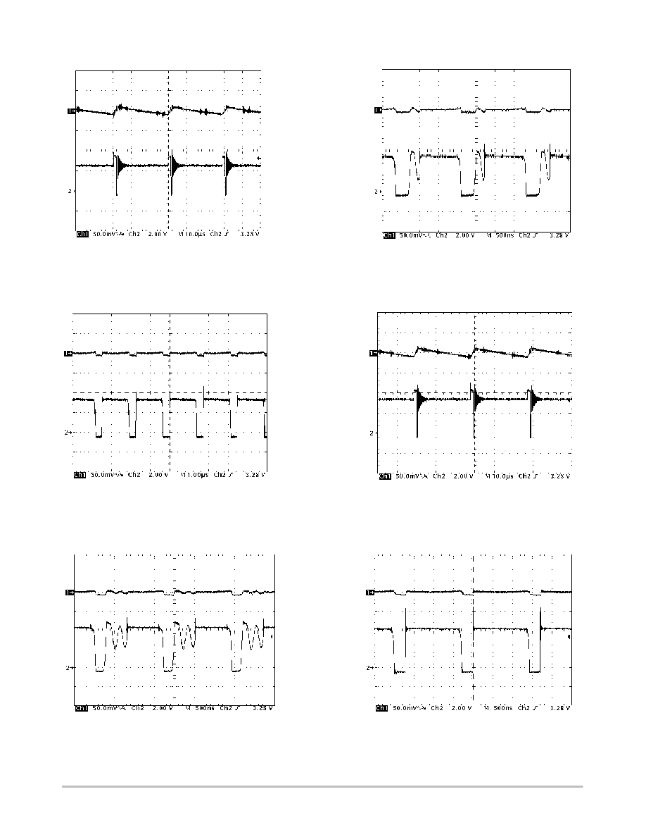
Upper Trace: Output Voltage Ripple, 50 mVac/Div.
Lower Trace: LX Pin Switching Waveform, 2.0 V/Div.
Figure 27. PFM Switching Waveform and
Output Ripple for V
OUT
= 2.5 V
(V
IN
= 3.5 V, V
OUT
= 2.5 V, I
LOAD
= 80 mA)
Upper Trace: Output Voltage Ripple, 50 mVac/Div.
Lower Trace: LX Pin Switching Waveform, 2.0 V/Div.
Figure 28. DCM PWM Switching Waveform
and Output Ripple for V
OUT
= 2.5 V
(V
IN
= 3.5 V, V
OUT
= 2.5 V, I
LOAD
= 600 mA)
Upper Trace: Output Voltage Ripple, 50 mVac/Div.
Lower Trace: LX Pin Switching Waveform, 2.0 V/Div.
Figure 29. CCM PWM Switching Waveform
and Output Ripple for V
OUT
= 2.5 V
(V
IN
= 4.3 V, V
OUT
= 3.3 V, I
LOAD
= 10 mA)
Upper Trace: Output Voltage Ripple, 50 mVac/Div.
Lower Trace: LX Pin Switching Waveform, 2.0 V/Div.
Figure 30. PFM Switching Waveform and
Output Ripple for V
OUT
= 3.3 V
(V
IN
= 4.3 V, V
OUT
= 3.3 V, I
LOAD
= 50 mA)
Upper Trace: Output Voltage Ripple, 50 mVac/Div.
Lower Trace: LX Pin Switching Waveform, 2.0 V/Div.
Figure 31. DCM PWM Switching Waveform
and Output Ripple for V
OUT
= 3.3 V
(V
IN
= 4.3 V, V
OUT
= 3.3 V, I
LOAD
= 600 mA)
Upper Trace: Output Voltage Ripple, 50 mVac/Div.
Lower Trace: LX Pin Switching Waveform, 2.0 V/Div.
Figure 32. CCM PWM Switching Waveform
and Output Ripple for V
OUT
= 3.3 V

NCP1530
http://onsemi.com
10
(V
IN
= 3.5 V, V
OUT
= 2.5 V, C
SS
= 100 pF, No load)
Upper Trace: Output Voltage, 2.0 V/Div.
Lower Trace: EN Pin Waveform, 2.0 V/Div.
Time Scale: 5.0 ms/Div.
Figure 33. Soft-Start Output Voltage
Waveform for V
OUT
= 2.5 V
(V
IN
= 4.3 V, V
OUT
= 3.3 V, C
SS
= 100 pF, No load)
Upper Trace: Output Voltage, 2.0 V/Div.
Lower Trace: EN Pin Waveform, 2.0 V/Div.
Time Scale: 5.0 ms/Div.
Figure 34. Soft-Start Output Voltage
Waveform for V
OUT
= 3.3 V

NCP1530
http://onsemi.com
11
DETAILED OPERATING DESCRIPTION
Introduction
The NCP1530 series are step-down converters with a
smart control scheme that operates with 600 kHz fixed
Pulse Width Modulation (PWM) at moderate to heavy load
currents, so that high efficiency, noise free output voltage
can be generated. In order to improve the system efficiency
at light loads, this device can be configured to work in
auto-mode. In auto-mode operation, the control unit will
detect the loading condition and switch to power saving
Pulse Frequency Modulation (PFM) control scheme at
light load. With these enhanced features, the converter can
achieve high operating efficiency for all loading
conditions. Additionally, the switching frequency can also
be synchronized to external clock signal in between
600 kHz to 1.2 MHz range. The converter uses peak
current mode PWM control as a core, with the high
switching frequency incorporated. Good line and load
regulation can be achieved easily with small value ceramic
input and output capacitors. Internal integrated
compensation voltage ramp ensures stable operation at all
operating modes. NCP1530 series are designed to support
up to 600 mA output current with cycle-by-cycle current
limit protection.
The Internal Oscillator
The oscillator that governs the switching of the PWM
control cycle is self contained and no external timing
component is required to setup the switching frequency.
For PWM mode and auto-mode operation, all timing
signals required for proper operation are derived from the
internal oscillator. The internal fix frequency oscillator is
trimmed to run at 600 kHz
" 20% over full temperature
range. In case the device is forced to operate at
Synchronization mode by applying an external clock signal
to SYN pin (pin 2), the external clock signal will supersede
the internal oscillator and take charge of the switching
operation.
Voltage Reference and Soft-Start
An internal high accuracy voltage reference is included
in NCP1530. This reference voltage governs all internal
reference levels in various functional blocks required for
proper operation. This reference voltage is precisely
trimmed to 1.2 V
" 1.5% over full temperature range. The
reference voltage can be accessed externally at V
REF
pin
(pin 7), with an external capacitor, C
REF
of 1.0
mF, privding
up to 5.0 mA of loading. Additionally, NCP1530 has a
Soft-Start circuit built around the voltage reference block
that provide limits to the inrush current during start-up by
controlling the ramp up of the internal voltage reference.
The soft-start time can be user adjusted by an external
capacitor, C
SS
, connecting to the SS pin (pin 3). During
converter powerup, a 50 nA current flowing out from the
SS pin will charge-up the timing capacitor. The voltage
across the SS pin controls the ramp up of the internal
reference voltage by slowly releasing it until the nominal
value is reached. For an external timing capacitor of value
C
SS
= 100 pF, the soft-start time is about 5.0 ms including
the small logic delay time, Figure 33 and 34. In the case
where the SS pin is left floating, a small built-in capacitor
together with other parasitic capacitance will provide a
minimum intrinsic soft-start time of 500
ms. As the
soft-start function is implemented by simple circuitry, the
final timing depends on non-linear functions, where
accurate deterination of the soft-start timing is impossible.
However, for simplicity, the empirical formula below can
be used to estimate the soft-start time with respect to the
value of the external capacitor.
tSS in
m
s
[
50
CSS in pF
)
500
m
s
Current Mode Pulse-Width Modulation (PWM)
Control Scheme
With the SYN pin (pin 2) connected to V
IN
, the converter
will set to operate at constant switching frequency PWM
mode. NCP1530 uses peak current mode control scheme to
achieve good line and load regulation. The high switching
frequency, 600 kHz, and a carefully compensated internal
control loop, allows the use of low profile small value
ceramic type input and output capacitor for stable
operation. In current mode operation, the required ramp
function is generated by sensing the inductor current
(ISEN) and comparing with the voltage loop error
amplifier (OTA) output. The OTA output is derived from
feedback from the output voltage pin (V
OUT
- Pin 6) and
the internal reference voltage (V
REF
- Pin 7). See Figure 2.
On a cycle-by-cycle basis, the duty cycle is controlled to
keep the output voltage within regulation. The current
mode approach has outstanding line regulation
performance and good overall system stability.
Additionally, by monitoring the inductor current, a
cycle-by-cycle current limit protection is implemented.
Constant Frequency PWM scheme reduces output ripple
and noise, which is one of the important characteristics for
noise sensitive communication applications. The high
switching frequency allows the use of small size surface
mount components that saves significant PC board area and
improves layout compactness and EMI performance.

NCP1530
http://onsemi.com
12
Power Saving Pulse-Frequency-Modulation (PFM)
Control Scheme
With the SYN pin (pin 2) connected to ground or left
open, the converter will operate in PWM/PFM auto mode.
Under this operating mode, NCP1530 will stay in constant
frequency PWM operation in moderate to heavy load
conditions. When the load decreases down to a threshold
point, the operation will switch to the power saving PFM
operation automatically. The switchover mechanism
depends on the input voltage, output voltage and the
inductor current level. The mode change circuit will
determine whether the converter should be operated in
PWM or PFM mode. In order to maintain stable and smooth
switching mode transition, a small hysteresis on the load
current level for mode transition was implemented. The
detailed mode transition characteristics for each voltage
option are illustrated in Figures 11 and 14. PFM mode
operation provides high conversion efficiency even at very
light loading conditions. In PFM mode, most of the circuits
inside the device will be turned off and the converter
operates just as a simple voltage hysteretic converter.
When the load current increases, the converter returns to
PWM mode automatically.
External Synchronization Control
The NCP1530 has an internal fixed frequency oscillator
of 600 kHz or can be synchronized to an external clock
signal at SYN pin (pin 2). Connecting the SYN pin with an
external clock signal will force the converter to operate in
a pure PWM mode and the switching frequency will be
synchronized. The external clock signal should be in the
range of 600 kHz to 1.2 MHz and the pulse width should
not be less than 300 ns. The detection of the pulse train is
edge sensitive and independent of duty ratio. In the case
where the external clock frequency is too low, the detection
circuit may not be able to follow and will treat it as a
disturbance, thus affecting the converters normal
operation. The internal control circuit detects the rising
edge of the pulse train and the switching frequency
synchronized to the external clock signal. If the external
clock signal ceases for several clock cycles, the converter
will switch back to use the internal oscillator automatically.
Power Saving Shutdown Mode
NCP1530 can be disabled whenever the EN pin (pin 5)
is tied to ground. In shutdown mode, the internal reference,
oscillator and most of the control circuitries are turned off.
With the device put in shutdown mode, the device current
consumption will be as low as 0.5
mA (typ).
Input Undervoltage Lockout Protection (UVLO)
To prevent the P-Channel MOSFETs from operating
below safe input voltage levels, an Undervoltage Lockout
protection is incorporated in NCP1530. Whenever the
input voltage, V
IN
drops below approximately 2.0 V, the
protection circuitry will be activated and the converter
operation will be stopped.
Output Overvoltage Protection (OVP)
In order to prevent the output voltage from going to high
(when the load current is close to zero in a pure PWM mode
and other abnormal conditions), an Output Overvoltage
protection circuit is included in the NCP1530. In case the
output voltage is higher than its nominal level by more than
12% maximum, the protection circuitry will stop the
switching immediately.
Internal Thermal Shutdown
Internal thermal shutdown circuitry is provided to
protect the integrated circuit in the event that the maximum
junction temperature is exceeded. The protection will be
activated at about 145
∞
C with a hysteresis of 15
∞
C. This
feature is provided to prevent failures from unexpected
overheating.
Input Capacitor Selection
For a PWM converter operating in continuous current
mode, the input current of the converter is a square wave
with a duty ratio of approximately V
OUT
/V
IN
. The
pulsating nature of the input current transient can be a
source of EMI noise and system instability. Using an input
bypass capacitor can reduce the peak current transients
drawn from the input supply source, thereby reducing
switching noise significantly. The capacitance needed for
the input bypass capacitor depends on the source
impedance of the input supply. For NCP1530, a low ESR,
low profile ceramic capacitor of 22
mF can be used for most
of the cases. For effective bypass results, the input
capacitor should be placed just next to V
IN
pin (pin 1)
whenever it is possible.
Inductor Value Selection
Selecting the proper inductance for the power inductor
is a trade-off between inductor's physical sizes, transient
response, power delivering capability, output voltage
ripple and power conversion efficiency. Low value
inductor saves cost, PC board space and provides fast
transient response, however suffers high inductor ripple
current, core loss and lower overall conversion efficiency.
The relationship between the inductance and the inductor
ripple current is given by the equation in below.
L
+
TON(VIN
*
RDS(ON)
IOUT
*
VF
*
VOUT)
IL_RIPPLE(P
*
P)
Where L is the inductance required;
T
ON
is the nominal ON time within a switching cycle;
R
DS(ON)
is the ON resistance of the internal MOSFET;
V
F
is the forward voltage drop of the Schottky diode;
V
IN
is the worst-case input voltage;
V
OUT
is the output voltage;
I
OUT
is the maximum allowed loading current;
I
L_RIPPLE(P-P)
is the acceptable inductor current ripple
level.

NCP1530
http://onsemi.com
13
For ease of application, the previous equation was
plotted in Figure 35 to help end user to select the right
inductor for specific application. As a rule of thumb, the
user needs to be aware of the maximum peak inductor
current and should be designed not to exceed the saturation
limit of the inductor selected. Low inductance can supply
higher output current, but suffers higher output ripple and
reduced efficiency, but it limits the output current
capability. On the other hand, high inductance can improve
output ripple and efficiency, at the same time, it also limits
the output current capability. One other critical parameter
of the inductor is its DC resistance. This resistance can
introduce unwanted power loss and hence reduce overall
efficiency. The basic rule is selecting an inductor with
lowest DC resistance within the board space limitation.
V
IN
, INPUT VOLTAGE (
V)
3.0 V
3.3 V
2.7 V
2.5 V
L, INDUCT
ANCE (
m
H)
0
2.0
4.0
6.0
8.0
10
12
3.0
3.5
4.0
4.5
5.0
Figure 35. Inductor Selection Chart
R
DS(ON)
= 3.0
W
D1, MBRM120ET3
C
IN
= C
OUT
= 22
m
F
I
OUT
= 600 mA
I
L_RIPPLE(P-P)
= 0.2 A
Flywheel Diode Selection
The flywheel diode is turned on and carries load current
during the off time. At high input voltages, the diode
conducts most of the time. In the case where V
IN
approaches V
OUT
,
the diode conducts only a small fraction
of the cycle. While the output terminals are shorted, the
diode will be subject to its highest stress. Under this
condition, the diode must be able to safely handle the peak
current circulating in the loop. So, it is important to select
a flywheel diode that can meet the diode peak current and
average power dissipation requirements. Under normal
conditions, the average current conducted by the flywheel
diode is given by,
ID
+
VIN
*
VOUT
VIN
)
VF
IOUT
Where I
D
is the average diode current and V
F
is the forward
voltage drop of the diode.
A low forward voltage drop and fast switching diode
must also be used to optimize converter efficiency.
Schottky diodes are a good choice for low forward drop and
fast switching times.
Output Capacitor Selection
Selection of the output capacitor, C
OUT
is primarily
governed by the required effective series resistance (ESR)
of the capacitor. Typically, once the ESR requirement is
met, the capacitance will be adequate for filtering. The
output voltage ripple, V
RIPPLE
is approximated by,
VRIPPLE
[
IL_RIPPLE(P
*
P)
ESR
)
1
4
FOSCCOUT
Where F
OSC
is the switching frequency and ESR is the
effective series resistance of the output capacitor.
From equation in above, it can be noted that the output
voltage ripple is contributed to by two parts. For most of the
cases, the major contributor is the capacitor's ESR.
Ordinary aluminum-electrolytic capacitors have high ESR
and should be avoided. High quality Low ESR
aluminum-electrolytic capacitors are acceptable and
relatively inexpensive. Low ESR tantalum capacitors are
another alternative. For even better performance, surface
mounted ceramic capacitors can be used. Ceramic
capacitors have lowest ESR among all choices. The
NCP1530 is internally compensated for stable operation
with low ESR ceramic capacitors. However, ordinary
multi-layer ceramic capacitors have poor temperature and
frequency performance, for switching applications, so only
high quality, grade X5R and X7R ceramic capacitors can
be used.
PCB Layout Recommendations
Good PCB layout plays an important role in switching
mode power conversion. Careful PCB layout can help to
minimize ground bounce, EMI noise and unwanted
feedbacks that can affect the performance of the converter.
Hints suggested below can be used as a guideline in most
situations.
Grounding
Star-ground connection should be used to connect the
output power return ground, the input power return ground
and the device power ground together at one point. All high
current running paths must be thick enough for current
flowing through and producing insignificant voltage drop
along the path.
Components Placement
Power components, i.e. input capacitor, inductor and
output capacitor, must be placed as close together as
possible. All connecting traces must be short, direct and
thick. High current flowing and switching paths must be
kept away from the feedback (V
OUT
, pin 6) terminal to
avoid unwanted injection of noise into the feedback path.
Feedback Path
Feedback of the output voltage must be a separate trace
separated from the power path. The output voltage sensing
trace to the feedback (V
OUT
, pin 6) pin should be connected
to the output voltage directly at the anode of the output
capacitor.

NCP1530
http://onsemi.com
14
ORDERING INFORMATION
Device
Output Voltage
Device Marking
Package
Shipping
NCP1530DM25R2
2.5 V
DAAA
NCP1530DM27R2
2.7 V
DAAB
Micro8
NCP1530DM30R2
3.0 V
DAAC
4000 Units
Per 7 Inch Reel
NCP1530DM30R2G
3.0 V
DAAC
Micro8
(Pb-Free)
Per 7 Inch Reel
NCP1530DM33R2
3.3 V
DAAD
Micro8
For information on tape and reel specifications, including part orientation and tape sizes, please refer to our Tape and Reel Packaging
Specifications Brochure, BRD8011/D.
NOTE:
The ordering information lists four standard output voltage device options. Additional device with output voltage ranging from 2.5 V to
3.5 V in 100 mV increments can be manufactured. Contact your ON Semiconductor representative for availability.
NCP1530
http://onsemi.com
15
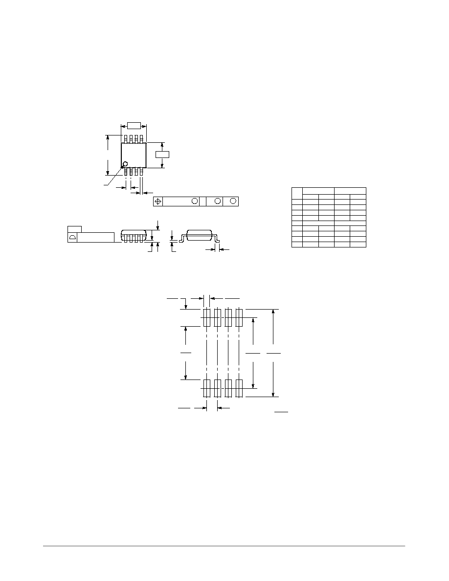
PACKAGE DIMENSIONS
Micro8
DM SUFFIX
CASE 846A-02
ISSUE F
S
B
M
0.08 (0.003)
A
S
T
DIM
MIN
MAX
MIN
MAX
INCHES
MILLIMETERS
A
2.90
3.10
0.114
0.122
B
2.90
3.10
0.114
0.122
C
---
1.10
---
0.043
D
0.25
0.40
0.010
0.016
G
0.65 BSC
0.026 BSC
H
0.05
0.15
0.002
0.006
J
0.13
0.23
0.005
0.009
K
4.75
5.05
0.187
0.199
L
0.40
0.70
0.016
0.028
NOTES:
1. DIMENSIONING AND TOLERANCING PER ANSI
Y14.5M, 1982.
2. CONTROLLING DIMENSION: MILLIMETER.
3. DIMENSION A DOES NOT INCLUDE MOLD
FLASH, PROTRUSIONS OR GATE BURRS. MOLD
FLASH, PROTRUSIONS OR GATE BURRS SHALL
NOT EXCEED 0.15 (0.006) PER SIDE.
4. DIMENSION B DOES NOT INCLUDE INTERLEAD
FLASH OR PROTRUSION. INTERLEAD FLASH OR
PROTRUSION SHALL NOT EXCEED 0.25 (0.010)
PER SIDE.
5. 846A-01 OBSOLETE, NEW STANDARD 846A-02.
-B-
-A-
D
K
G
PIN 1 ID
8 PL
0.038 (0.0015)
-T-
SEATING
PLANE
C
H
J
L
*For additional information on our Pb-Free strategy and soldering
details, please download the ON Semiconductor Soldering and
Mounting Techniques Reference Manual, SOLDERRM/D.
SOLDERING FOOTPRINT*
8X
8X
6X
mm
inches
SCALE 8:1
1.04
0.041
0.38
0.015
5.28
0.208
4.24
0.167
3.20
0.126
0.65
0.0256

NCP1530
http://onsemi.com
16
ON Semiconductor and are registered trademarks of Semiconductor Components Industries, LLC (SCILLC). SCILLC reserves the right to make changes without further notice
to any products herein. SCILLC makes no warranty, representation or guarantee regarding the suitability of its products for any particular purpose, nor does SCILLC assume any
liability arising out of the application or use of any product or circuit, and specifically disclaims any and all liability, including without limitation special, consequential or incidental
damages. "Typical" parameters which may be provided in SCILLC data sheets and/or specifications can and do vary in different applications and actual performance may vary over
time. All operating parameters, including "Typicals" must be validated for each customer application by customer's technical experts. SCILLC does not convey any license under
its patent rights nor the rights of others. SCILLC products are not designed, intended, or authorized for use as components in systems intended for surgical implant into the body,
or other applications intended to support or sustain life, or for any other application in which the failure of the SCILLC product could create a situation where personal injury or death
may occur. Should Buyer purchase or use SCILLC products for any such unintended or unauthorized application, Buyer shall indemnify and hold SCILLC and its officers, employees,
subsidiaries, affiliates, and distributors harmless against all claims, costs, damages, and expenses, and reasonable attorney fees arising out of, directly or indirectly, any claim of
personal injury or death associated with such unintended or unauthorized use, even if such claim alleges that SCILLC was negligent regarding the design or manufacture of the part.
SCILLC is an Equal Opportunity/Affirmative Action Employer. This literature is subject to all applicable copyright laws and is not for resale in any manner.
PUBLICATION ORDERING INFORMATION
N. American Technical Support: 800-282-9855 Toll Free
USA/Canada
Japan: ON Semiconductor, Japan Customer Focus Center
2-9-1 Kamimeguro, Meguro-ku, Tokyo, Japan 153-0051
Phone: 81-3-5773-3850
NCP1530/D
Micro8 is a trademark of International Rectifier.
LITERATURE FULFILLMENT:
Literature Distribution Center for ON Semiconductor
P.O. Box 61312, Phoenix, Arizona 85082-1312 USA
Phone: 480-829-7710 or 800-344-3860 Toll Free USA/Canada
Fax: 480-829-7709 or 800-344-3867 Toll Free USA/Canada
Email: orderlit@onsemi.com
ON Semiconductor Website: http://onsemi.com
Order Literature: http://www.onsemi.com/litorder
For additional information, please contact your
local Sales Representative.