
©
Semiconductor Components Industries, LLC, 2004
August, 2004 - Rev. 3
1
Publication Order Number
NCP1561/D
NCP1561
Push-Pull PWM Controller
for 48 V Telecom Systems
The NCP1561 Push-Pull PWM controller contains all the features
and flexibility needed to implement high efficiency dc-dc converters
using voltage or current-mode control. This device can be configured
in any dual ended topology such as push-pull or half-bridge. It can
also be used for forward topologies requiring a 50% maximum duty
cycle. This device is ideally suited for 48 V telecom, 42 V automotive
systems and 12 V input applications.
The NCP1561 cost effectively reduce system part count by
incorporating a high voltage startup regulator, line undervoltage
detector, single resistor oscillator setting, dual mode overcurrent
protection, soft-start and single resistor feedforward ramp generator.
The oscillator frequency can be adjusted up to 250 kHz.
Features
∑
Internal High Voltage Startup Regulator
∑
Minimum Operating Voltage of 21.5 V
∑
Voltage or Current-Mode Control Capability
∑
Single Resistor Oscillator Frequency Setting
∑
Adjustable Frequency up to 250 kHz
∑
Fast Line Feedforward
∑
Line Undervoltage Lockout
∑
Dual Mode Overcurrent Protection
∑
Programmable Maximum Duty Cycle Control
∑
Maximum Duty Cycle Proportional to Line Voltage
∑
Programmable Soft-Start
∑
Precision 5.0 V Reference
Typical Applications
∑
48 V Telecommunication Power Converters
∑
Industrial Power Converters
∑
42 V Automotive Systems
Figure 1. Half-Bridge Block Diagram
Vin
TX1
M1
Lout
Cout
NCP1561
+
-
M2
Opto
Error
Amplifier
Driver
High Side
Driver
M3
OUT1
OUT1
OUT2
Startup
Feedforward
OUT2
M4
C1
C2
Device
Package
Shipping
ORDERING INFORMATION
NCP1561DR2
SO-16
2500 Units/Reel
NCP1561 = Device Code
A
= Assembly Location
WL
= Wafer Lot
Y
= Year
WW
= Work Week
MARKING
DIAGRAM
16
SO-16
D SUFFIX
CASE 751B
NCP1561
1
1
16
AWLYWW
PIN ASSIGNMENTS
V
in
V
AUX
UV
OUT1
RAMP_OUT
GND
FF
OUT2
CS
RAMP_IN
CSKIP
V
REF
R
T
V
EA
DC
MAX
SS
For information on tape and reel specifications,
including part orientation and tape sizes, please
refer to our Tape and Reel Packaging Specification
Brochure, BRD8011/D.
http://onsemi.com

NCP1561
http://onsemi.com
2
V
in
GND
UV
CS
FF
High Voltage
Startup
Regulator
Fault
Detection
Oscillator
Modulator
Figure 2. Simplified Block Diagram
Thermal
Shutdown
5.0 V
Reference
V
AUX
SS
V
EA
R
T
Output
Stage
OUT1
OUT2
UV
DC
MAX
V
REF
CSKIP
RAMP_OUT
RAMP_IN

NCP1561
http://onsemi.com
3
Figure 3. NCP1561 Block Diagram
V
EA
-
+
-
+
CS
S
R
Q
Reset
Dominant
Latch
C
SS
10
5
12
STOP
C
CSKIP
Clock
Enable_ss
10.8 pF
FF Ramp
(Adjustable)
* Trimmed during
manufacturing to obtain
1.3 V with R
T
= 101 k
W
V
in
R
FF
FF
4
+
CURRENT MIRROR
-
+
2 V
10 pF
I
1
+
-
-
2 V
7
Oscillator Ramp
2 V
+
-
8
2 V
Max DC
Comparator
PWM
Comparator
+
-
Softstart
Comparator
1.0 V
+
-
1.2 V
+
-
SS
9
One Shot
Pulse
-
+
6
-
+
2 V
+
-
2
1.3 V*
RAMP_IN
V
REF
DC
MAX
+
V
DC(inv)
-
R
MDP
R
P
C
FF
I
FF
Disable
+
V
-
-
+
R
T
(600 ns)
One Shot
Pulse
Clock
TF/F
Q
OUT1
OUT2
15
13
3
RAMP_OUT
Buffer
V
AUX
V
AUX
CSKIP
I
1
R
T
Q
6.7 k
W
5.3 k
W
V
REF
12
m
A
2 k
W
20 k
W
29 k
W
29 k
W
38 k
W
V
REF
I
+
V
125 k
W
+
-
+
-
5.0 V Reference
Vin
16
1
11
STOP
Disable
S
R
Q
Dominant
Reset
Latch
(250 ns)
DIS
2
UV
One Shot
Pulse
+
-
Thermal
Shutdown
-
+
+
-
1.52 V
+
-
V
AUX
C
AUX
V
in
I
AUX
V
AUX
Enable_ss
V
AUX(on)
V
REF
Disable_V
REF
V
AUX(on)
/V
AUX(off)
Output Latch
6
m
A
V
REF
R
EA

NCP1561
http://onsemi.com
4
PIN DESCRIPTION
Pin
Name
Application Information
1
V
in
This pin is connected to the bulk DC input voltage supply. A constant current source supplies current from
this pin to the capacitor connected on the V
AUX
pin. The charge current is typically 13.0 mA. Input voltage
range is 21.5 V to 150 V.
2
UV
Input supply voltage is scaled down and sampled by means of a resistor divider. The supply voltage must be
scaled such that the voltage on the UV pin is 1.54 V at the minimum input voltage.
3
RAMP_OUT
Internal Feedforward (FF) Ramp Output. This signal can be externally routed to the RAMP_IN pin for
voltage-mode control operation.
4
FF
An external resistor between V
in
and this pin adjusts the amplitude of the FF Ramp inversely proportional to
V
in
. By varying the Feedforward Ramp amplitude in proportion to the input voltage, changes in loop
bandwidth resulting from V
in
changes are eliminated.
5
CS
Overcurrent sense input. If the CS voltage exceeds 0.95 V or 1.15 V, the converter enters the Cycle by Cycle
or Cycle Skip current limit mode, respectively.
6
CSKIP
The capacitor connected to this pin sets the Cycle Skip period. Once a cycle skip fault is detected, the
capacitor connected to this pin is discharged. The capacitor is then charged with a constant current of 12
m
A.
The cycle skip period expires, once the voltage on this capacitor reaches 2.0 V. A soft-start sequence follows
at the conclusion of the fault period.
7
R
T
A single external resistor between this pin and GND sets the fixed oscillator frequency.
8
DC
MAX
An external resistor between this pin and GND sets the voltage on the Max DC Comparator inverting input.
The duty cycle is limited by comparing the voltage on the Max DC Comparator inverting input to the
Feedforward Ramp.
9
SS
An internal 6.0
m
A current source charges the external capacitor connected to this pin. The duty cycle is
limited during startup by comparing the voltage on this pin to the Oscillator Ramp. The soft-start comparator
limits the duty cycle while the SS voltage is below 2.0 V.
10
V
EA
The error signal from an external error amplifier is fed into this input and compared to the Feedforward Ramp.
A series diode and resistor offset the voltage on this pin before it is applied to the PWM Comparator inverting
input.
11
V
REF
Precision 5.0 V reference output. Maximum output current is 6.0 mA.
12
RAMP_IN
This pin configures the NCP1561 for voltage or current-mode control. The internal Feedforward Ramp
(voltage-mode) or a signal proportional to the inductor current (current-mode) is fed into this input and
compared to the signal in the V
EA
pin.
13
OUT2
Output 2.
14
GND
Control circuit ground.
15
OUT1
Output 1.
16
V
AUX
Positive input supply voltage. This pin is connected to an external capacitor for energy storage. An internal
current source supplies current from V
in
to this pin. Once the voltage on V
AUX
reaches approximately 10.3 V,
the current source turns OFF. It turns ON again once V
AUX
falls to 7 V. During normal operation, power is
supplied to the IC via this pin, by means of an auxiliary winding. The startup circuit is disabled if the voltage
on the V
AUX
pin exceeds 10.3 V.

NCP1561
http://onsemi.com
5
MAXIMUM RATINGS
(Note 1)
Rating
Symbol
Value
Unit
Input Line Voltage
V
in
-0.3 to 150
V
Auxiliary Supply Voltage
V
AUX
-0.3 to 16
V
Auxiliary Supply Input Current
I
AUX
35
mA
OUT1 and OUT2 Voltage
V
OUT
-0.3 to (V
AUX
+ 0.3 V)
V
OUT1 and OUT2 Output Current
I
OUT
10
mA
5.0 V Reference Voltage
V
REF
-0.3 to 6.0
V
5.0 V Reference Output Current
I
REF
6.0
mA
All Other Inputs/Outputs Voltage
V
IO
-0.3 to V
REF
V
All Other Inputs/Outputs Current
I
IO
10
mA
Operating Junction Temperature
T
J
-40 to 150
_
C
Storage Temperature Range
T
stg
-55 to 150
_
C
Power Dissipation at T
A
= 25
∞
C
P
D
0.77
W
Thermal Resistance, Junction-to-Ambient
R
JA
130
_
C/W
1. Maximum ratings are those values beyond which device damage can occur. Maximum ratings applied to the device are individual stress limit
values (not normal operating conditions) and are not valid simultaneously. If these limits are exceeded, device functional operation is not
implied, damage may occur and reliability may be affected.
A. This device series contains ESD protection and exceeds the following tests:
Pin 1: Pin 1 is the HV start-up of the device and is rated to the max rating of the part, or 150 V.
Machine Model Method 150 V.
Pins 2-16: Human Body Model 2000 V per MIL-STD-883, Method 3015.
Machine Model Method 200 V.
NCP1561
http://onsemi.com
6
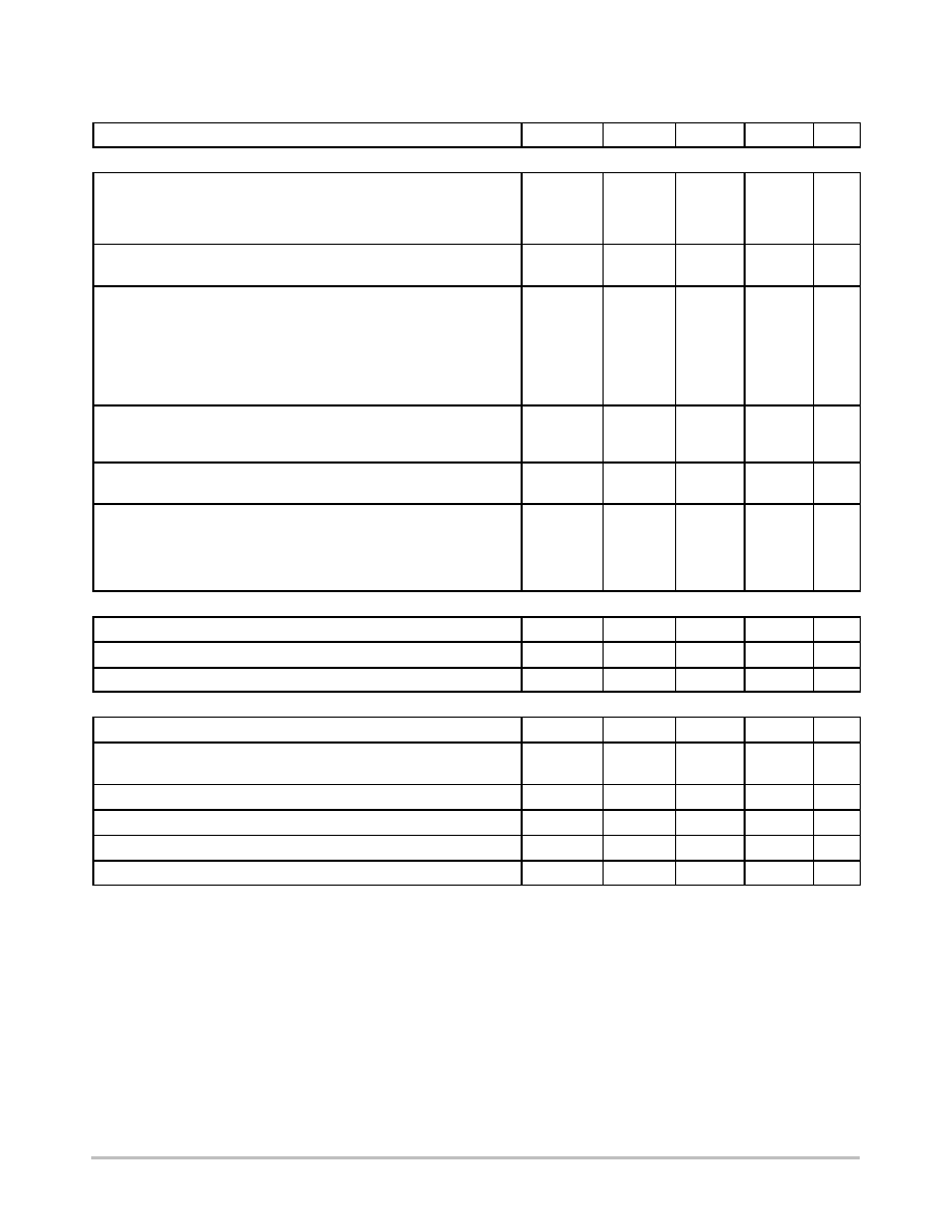
ELECTRICAL CHARACTERISTICS
(V
in
= 48 V, V
AUX
= 12 V, V
EA
= 2 V, R
T
= 101 k
W
,
C
CSKIP
= 6800 pF, R
D
= 60.4 k
W
,
R
FF
= 432 k
W
, for typical values T
J
= 25
∞
C, for min/max values, T
J
= -40
∞
C to 125
∞
C, unless otherwise noted)
Characteristic
Symbol
Min
Typ
Max
Unit
START-UP CONTROL AND V
AUX
REGULATOR
V
AUX
Regulation
Startup Threshold/V
AUX
Regulation Peak (V
AUX
increasing)
Minimum Operating V
AUX
Valley Voltage After Turn-On
Hysteresis
V
AUX(on)
V
AUX(off)
V
H
9.7
6.6
-
10.3
7.0
3.3
10.8
7.4
-
V
Minimum Startup Voltage (Pin 1)
I
START
= 1.0 mA, I
REF
= 0 mA, V
AUX
= V
AUX(on)
- 0.2 V
V
START(min)
-
18.3
21.5
V
Startup Circuit Output Current
V
AUX
= 0 V
T
J
= 25
∞
C
T
J
= -40
∞
C to 125
∞
C
V
AUX
= V
AUX(on)
- 0.2 V
T
J
= 25
∞
C
T
J
= -40
∞
C to 125
∞
C
I
START
13
10
10
8.0
17
-
13
-
21
25
17
19
mA
Startup Circuit Off-State Leakage Current (V
in
= 150 V)
T
J
= 25
∞
C
T
J
= -40
∞
C to 125
∞
C
I
START(off)
-
-
23
-
50
100
m
A
Startup Circuit Breakdown Voltage (Note 2)
I
START(off)
= 50
m
A, T
J
= 25
∞
C
V
BR(DS)
150
-
-
V
Auxilliary Supply Current After V
AUX
Turn-On
Outputs Disabled
V
EA
= 0 V
V
UV
= 0 V
Outputs Enabled
I
AUX1
I
AUX2
I
AUX3
-
-
-
3.3
1.8
4.1
5.0
2.5
6.5
mA
LINE UNDERVOLTAGE DETECTOR
Undervoltage Threshold (V
in
Increasing)
V
UV
1.40
1.54
1.64
V
Undervoltage Hysteresis
V
UV(H)
0.080
0.095
0.120
V
Undervoltage Propagation Delay to Output
t
UV
-
250
-
ns
CURRENT LIMIT AND THERMAL SHUTDOWN
Cycle by Cycle Threshold Voltage
I
LIM1
0.89
0.95
1.03
V
Propagation Delay to Output (V
EA
= 2.0 V)
V
CS
= I
LIM1
to 2.0 V, measured when OUT1 reaches 10 V.
t
ILIM
-
86
150
ns
Cycle Skip Threshold Voltage
I
LIM2
1.05
1.15
1.24
V
Cycle Skip Charge Current (V
CSKIP
= 0 V)
I
CSKIP
8.0
12.3
15
m
A
Thermal Shutdown Threshold (Junction Temperature Increasing, Note 2)
T
SHDN
-
180
-
∞
C
Thermal Shutdown Hysteresis (Junction Temperature Decreasing, Note 2)
T
H
-
17
-
∞
C
2. Guaranteed by design only.

NCP1561
http://onsemi.com
7
ELECTRICAL CHARACTERISTICS
(V
in
= 48 V, V
AUX
= 12 V, V
EA
= 2 V, R
T
= 101 k
W
,
C
CSKIP
= 6800 pF, R
D
= 60.4 k
W
,
R
FF
= 432 k
W
, for typical values T
J
= 25
∞
C, for min/max values, T
J
= -40
∞
C to 125
∞
C, unless otherwise noted) (continued)
Characteristic
Symbol
Min
Typ
Max
Unit
CONTROL OUTPUTS
Frequency (R
T
= 101 k
W
)
T
J
= 25
∞
C
T
J
= -40
∞
C to 125
∞
C
f
OSC1
143
137
150
-
157
163
kHz
Frequency (R
T
= 59 k
W
)
T
J
= 25
∞
C
T
J
= -40
∞
C to 125
∞
C
f
OSC2
228
220
240
-
252
260
kHz
Output Voltage (I
OUT
= 0 mA)
Low State
High State
V
OL
V
OH
-
-
0.25
11.8
-
-
V
Drive Resistance (V
in
= 15 V)
Sink (V
EA
= 0 V, V
OUT
= 2 V)
Source (V
EA
= 3 V, V
OUT
= 10 V)
R
SNK
R
SRC
20
50
36
88
80
170
W
Rise Time (C
L
= 100 pF, 10% to 90% of V
OH
)
t
on
-
32
-
ns
Fall Time (C
L
= 100 pF, 90% to 10% of V
OH
)
t
off
-
19
-
ns
MAXIMUM DUTY CYCLE COMPARATOR
Maximum Duty Cycle (V
in
= 36 V)
R
P
= 0
W
, R
MDP
= open
R
P
= open, R
MDP
= open (Note 3)
DC
MAX
34
48
38
-
44
50
%
Open Circuit Voltage
V
DCMAX
0.49
0.74
0.90
V
SOFT-START
Charge Current (V
SS
= 1.0 V)
I
SS(C)
5.0
6.2
7.4
m
A
Discharge Current (V
SS
= 5.0 V, V
UV
= 1.0 V)
I
SS(D)
20
50
-
mA
PWM COMPARATOR
Input Resistance (V
1
= 1.25 V, V
2
= 1.50 V)
R
IN(VEA)
= (V
2
- V
1
) / (I
2
- I
1
)
R
IN(VEA)
8.0
22
60
k
W
Lower Input Threshold
V
EA(L)
0.7
0.92
1.1
V
Delay to Output (from V
OH
to 0.5 V
OH
)
t
PWM
-
200
-
ns
5.0 V REFERENCE
Output Voltage (I
REF
= 0 mA)
T
J
= 25
∞
C
T
J
= -40
∞
C to 125
∞
C
V
REF
4.9
4.8
4.96
-
5.1
5.1
V
Load Regulation (I
REF
= 0 to 6 mA)
V
REF(Load)
-
10
50
mV
Line Regulation (V
AUX
= 7.5 V to 16 V)
V
REF(Line)
-
50
100
mV
3. 50% Maximum Duty Cycle guaranteed by design.

NCP1561
http://onsemi.com
8
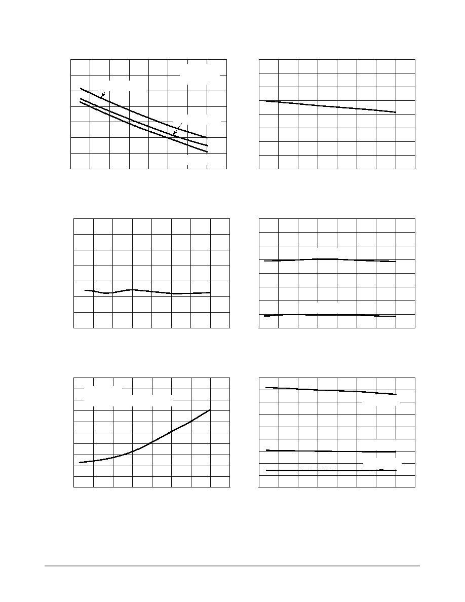
TYPICAL CHARACTERISTICS
Figure 4. Auxiliary Supply Voltage Thresholds
versus Junction Temperature
Figure 5. Startup Circuit Output Current
versus Junction Temperature
T
J
, JUNCTION TEMPERATURE (
∞
C)
T
J
, JUNCTION TEMPERATURE (
∞
C)
125
100
75
50
25
0
-25
-50
5
6
7
8
9
10
11
12
125
100
75
50
25
0
-25
-50
9
10
11
12
13
14
15
19
Figure 6. Startup Circuit Output Current
versus Auxiliary Supply Voltage
Figure 7. Startup Circuit Output Current
versus Line Voltage
V
AUX
, AUXILIARY SUPPLY VOLTAGE (V)
V
in
, LINE VOLTAGE (V)
12
10
8
6
4
2
0
12.5
13.0
14.5
15.0
15.5
16.0
16.5
17.5
150
125
100
75
50
25
0
0
4
8
12
16
20
Figure 8. Startup Circuit Off-State Leakage
Current versus Line Voltage
Figure 9. Auxiliary Supply Current versus
Junction Temperature
V
in
, LINE VOLTAGE (V)
T
J
, JUNCTION TEMPERATURE (
∞
C)
150
125
100
75
50
25
0
0
5
10
15
20
25
30
40
125
100
75
50
25
0
-25
-50
4.5
0.5
1.0
1.5
2.0
2.5
3.5
4.0
V
AUX
, AUXILIAR
Y SUPPL
Y VOL
T
AGE (V)
150
150
16
17
18
I
ST
AR
T
, ST
AR
TUP CIRCUIT OUTPUT
CURRENT (mA)
17.0
I
ST
AR
T
, ST
AR
TUP CIRCUIT OUTPUT
CURRENT (mA)
I
ST
AR
T
, ST
AR
TUP CIRCUIT OUTPUT
CURRENT (mA)
35
I
ST
AR
T(
of
f)
, ST
AR
TUP CIRCUIT OFF-
ST
A
TE LEAKAGE CURRENT (
m
A)
150
3.0
I
AUX
, AUXILIAR
Y SUPPL
Y CURRENT (mA)
STARTUP
THRESHOLD
MINIMUM
OPERATING
THRESHOLD
V
AUX
= 0 V
V
AUX
= V
AUX(on)
- 0.2 V
T
J
= -40
∞
C
T
J
= 25
∞
C
T
J
= 125
∞
C
T
J
= -40
∞
C
T
J
= 25
∞
C
T
J
= 125
∞
C
V
EA
= 0 V
V
UV
= 0 V
V
AUX
= 12 V
V
in
= 48 V
V
in
= 48 V
V
AUX
= V
AUX(on)
- 0.2 V
V
AUX
= 12 V
14.0
13.5
NCP1561
http://onsemi.com
9
TYPICAL CHARACTERISTICS
Figure 10. Operating Auxiliary Supply Current
versus Junction Temperature
Figure 11. Line Undervoltage Threshold
versus Junction Temperature
T
J
, JUNCTION TEMPERATURE (
∞
C)
T
J
, JUNCTION TEMPERATURE (
∞
C)
125
100
75
50
25
0
-25
-50
2.5
3.0
3.5
4.0
4.5
5.0
5.5
6.0
125
100
75
50
25
0
-25
-50
1.30
1.35
1.40
1.45
1.50
1.70
Figure 12. Line Undervoltage Hysteresis versus
Junction Temperature
T
J
, JUNCTION TEMPERATURE (
∞
C)
150
125
100
25
0
-25
-50
70
80
90
100
110
120
140
Figure 13. Current Limit Thresholds versus
Junction Temperature
T
J
, JUNCTION TEMPERATURE (
∞
C)
125
100
75
50
25
0
-25
-50
0.90
0.95
1.00
1.05
1.10
1.15
1.25
1.30
I
AUX3
, OPERA
TING AUXILIAR
Y
SUPPL
Y CURRENT (mA)
150
150
1.55
1.60
1.65
V
UV
, LINE UNDER
VOL
T
AGE
THRESHOLD (V)
130
V
UV(H)
, LINE UNDER
VOL
T
AGE
THRESHOLD HYSTERESIS (mV)
150
1.20
I
LIM
, CURRENT LIMIT THRESHOLDS (V)
75
50
f
OSC
= 250 kHz
CYCLE SKIP
CYCLE BY CYCLE
V
AUX
= 12 V
DC
[
50%
f
OSC
= 150 kHz
f
OSC
= 100 kHz
Figure 14. Current Limit Propagation Delay
versus Junction Temperature
T
J
, JUNCTION TEMPERATURE (
∞
C)
125
100
75
50
25
0
-25
-50
70
75
80
85
90
95
115
120
t
ILIM
, CURRENT LIMIT
PROP
AGA
TION DELA
Y (ns)
150
100
105
110
V
AUX
= 12 V
Measured from V
OH
to 0.5 V
OH
Figure 15. Oscillator Frequency versus
Junction Temperature
T
J
, JUNCTION TEMPERATURE (
∞
C)
125
100
75
50
25
0
-25
-50
75
100
125
150
175
200
300
150
225
250
275
f
osc
, OSCILLA
T
OR FREQUENCY (kHz)
R
T
= 148 k
W
R
T
= 101 k
W
R
T
= 50.6 k
W

NCP1561
http://onsemi.com
10
TYPICAL CHARACTERISTICS
Figure 16. Oscillator Frequency versus
Junction Temperature
Figure 17. Oscillator Frequency versus
Timing Resistor
R
T
, TIMING RESISTOR (k
W
)
400
300
250
200
150
100
50
0
50
100
150
200
300
250
f
osc
, OSCILLA
T
OR FREQUENCY (kHz)
350
T
J
, JUNCTION TEMPERATURE (
∞
C)
125
100
75
50
25
0
-25
-50
142.5
145.0
147.5
150.0
152.5
155.0
150
157.5
f
osc
, OSCILLA
T
OR FREQUENCY (kHz)
R
T
= 101 k
W
T
J
= 25
∞
C
DC
[
50%
T
J
, JUNCTION TEMPERATURE (
∞
C)
150
125
100
25
0
-25
-50
20
30
40
50
60
70
100
120
110
R
SNK/SRC
OUTPUTS DRIVE RESIST
ANCE (
W
)
50
75
80
90
R
SRC
(V
EA
= 0 V, V
OUT
= 10 V)
R
SNK
(V
EA
= 3 V, V
OUT
= 2 V)
V
AUX
= 12 V
Figure 18. Outputs Drive Resistance versus
Junction Temperature
Figure 19. Outputs Rise Time versus Load
Capacitance
C
L
, LOAD CAPACITANCE (pF)
200
150
100
50
0
0
10
20
30
40
50
60
80
70
t
on
, OUTPUTS RISE TIME (ns)
T
J
= -40
∞
C
T
J
= 25
∞
C
T
J
= 125
∞
C
175
125
75
25
Measured from 10% to 90% of V
OH
V
AUX
= 12 V
Figure 20. Outputs Fall Time versus Load
Capacitance
C
L
, LOAD CAPACITANCE (pF)
200
150
100
50
0
0
5
10
15
20
25
35
30
t
of
f
, OUTPUTS F
ALL TIME (ns)
T
J
= -40
∞
C
T
J
= 25
∞
C
T
J
= 125
∞
C
175
125
75
25
Measured from 90% to 10% of V
OH
V
AUX
= 12 V
Figure 21. Feedforward Internal Resistance
versus Junction Temperature
150
125
100
75
0
-25
-50
9
10
11
12
13
14
15
19
17
FEEDFOR
W
ARD INTERNAL RESIST
ANCE (k
W
)
50
25
16
18
T
J
, JUNCTION TEMPERATURE (
∞
C)

NCP1561
http://onsemi.com
11
TYPICAL CHARACTERISTICS
T
J
, JUNCTION TEMPERATURE (
∞
C)
125
100
75
50
25
0
-25
-50
3.0
3.5
4.0
4.5
5.0
5.5
6.5
7.0
150
6.0
I
SS(
C)
, SOFT-ST
AR
T CHARGE CURRENT (
m
A)
30
35
40
45
50
55
65
70
60
CHARGE
DISCHARGE
525
450
225
150
75
0
0
5
10
20
30
45
DC
MAX
, MAXIMUM DUTY CYCLE (%)
375
300
15
25
T
J
= -40
∞
C
T
J
= 125
∞
C
40
35
V
EA
= 3.0 V
DC
MAX
PIN = OPEN
T
J
, JUNCTION TEMPERATURE (
∞
C)
150
125
100
75
0
-25
-50
20
25
35
40
45
50
DC
MAX
, MAXIMUM DUTY CYCLE (%)
50
25
R
P
= OPEN, R
MDP
= OPEN
R
P
= 0
W
, R
MDP
= OPEN
V
in
= 36 V
R
FF
= 432 k
W
Figure 22. Maximum Duty Cycle versus
Feedforward Current
Figure 23. Maximum Duty Cycle versus
Junction Temperature
Figure 24. Soft-Start Charge/Discharge
Currents versus Junction Temperature
I
SS(
D)
, SOFT-ST
AR
T DISCHARGE CURRENT (mA)
I
FF
, FEEDFORWARD CURRENT (
m
A)
50
30
Figure 25. V
EA
Input Resistance versus
Junction Temperature
T
J
, JUNCTION TEMPERATURE (
∞
C)
150
100
50
0
-50
0
10
20
40
50
30
R
IN(
VEA)
, V
EA
INPUT RESIST
ANCE (k
W
)
-25
125
75
25
T
J
, JUNCTION TEMPERATURE (
∞
C)
150
125
100
25
0
-25
-50
0.75
0.80
0.85
0.95
1.00
V
EA(
L)
, PWM COMP
ARA
T
OR LOWER
INPUT THRESHOLD (V)
50
75
0.90
Figure 26. PWM Comparator Lower Input
Threshold versus Junction Temperature
T
J
, JUNCTION TEMPERATURE (
∞
C)
125
100
75
50
25
0
-25
-50
4.91
4.93
4.95
4.97
5.01
150
V
REF
, REFERENCE VOL
T
AGE (V)
I
REF
= 0 mA
I
REF
= 6 mA
4.99
Figure 27. Reference Voltage versus Junction
Temperature
R
FF
= 432 k
W
V
in
= 48 V

NCP1561
http://onsemi.com
12
DETAILED OPERATING DESCRIPTION
The NCP1561 is a push-pull PWM controller for use in
48 V telecom power converters or 42 V automotive
systems. This controller contains all the features and
flexibility required in high density isolated dc-dc modules
and on-board designs for telecom and automotive systems.
It can be configured for operation in voltage-mode with
feedforward or current-mode control. The extensive set of
features included in the NCP1561 facilitates system design
and reduces overall system cost and component count by
incorporating supervisory functions and components
traditionally found outside the controller. Features of the
NCP1561 include a high voltage startup regulator, fast line
feedforward, a line undervoltage lockout, dual mode
overcurrent protection, programmable maximum duty cycle
limit, programmable soft start and external voltage
reference.
Voltage-mode operation with line feedforward provides
better line regulation without some of the traditional
problems associated with current-mode control. The
controller is configured for voltage-mode operation by
routing the internal Feedforward Ramp output
(RAMP_OUT) to the PWM Comparator non-inverting
input (RAMP_IN). The amplitude of the Feedforward Ramp
varies inversely proportional to the input voltage. Operation
in current-mode control is obtained by routing a signal
proportional to the inductor current into the PWM
Comparator non-inverting input (V
EA
pin). In either mode,
the maximum duty cycle is inversely proportional to the line
voltage, as configured by the DC
MAX
pin and FF pins.
High Voltage Start-up Regulator
The NCP1561 contains an internal high voltage start-up
regulator that eliminates the need for external start-up
components. In addition, this regulator increases the
efficiency of the supply as it uses no power when in the
normal mode of operation, but instead uses power supplied
by an auxiliary winding. The startup regulator consists of a
constant current source that supplies current from the input
line voltage (V
in
) to the capacitor on the V
AUX
pin (C
AUX
).
The startup current is typically 13.0 mA. Once V
AUX
reaches approximately 10.3 V, the start-up regulator turns
OFF and the outputs are enabled. When V
AUX
reaches 7 V,
the outputs are disabled and the startup regulator turns ON.
This mode of operation is known as Dynamic Self Supply
(DSS).
The startup circuit sources current out of the V
AUX
pin. It
is recommended to place a diode between C
AUX
and the
auxiliary supply as shown in Figure 28. This will allow the
NCP1561 to charge C
AUX
while preventing the startup
regulator from sourcing current into the auxiliary supply.
Figure 28. Recommended V
AUX
Configuration
I
START
Disable
C
AUX
I
supply
V
AUX
I
AUX
To auxiliary supply
V
in
I
START
Power to the controller while operating in the self-bias or
DSS mode is provided by C
AUX
. Therefore, C
AUX
must be
sized such that a V
AUX
voltage greater than 7 V is
maintained while the outputs are enabled and the converter
reaches regulation. Also, the V
AUX
discharge time (from
10.3 V to 7 V) must be greater than the soft-start charge
period to assure the converter turns ON. The startup circuit
is rated at a maximum voltage of 150 V. If the device
operates in the DSS mode, power dissipation should be
controlled to avoid exceeding the maximum power
dissipation of the controller.
The startup regulator is disabled by biasing V
AUX
above
7 V once the outputs are enabled. It can also be disabled by
biasing V
AUX
above V
AUX(on)
(typically 10.3 V). This
feature allows the NCP1561 to operate from an independent
12 V (
±
10%) supply. The independent supply should keep
V
AUX
above V
AUX(on)
. Otherwise the Output Latch will not
be SET and the outputs will remain OFF after a fault
condition is cleared. If operating from an independent
supply, the V
in
and V
AUX
pins should be connected together.
NCP1561
http://onsemi.com
13
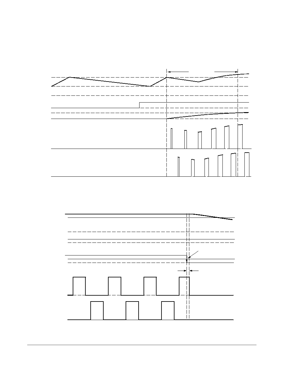
Line Undervoltage Shutdown
The NCP1561 incorporates a line undervoltage shutdown
(UV) circuit. The undervoltage threshold is approximately
1.54 V.
The UV circuit can be biased using an external resistor
divider from the input line. The resistor divider must be
sized to enable the controller once V
in
is within the required
operating range.
Once the UV condition is removed and V
AUX
reaches
V
AUX(on)
, the controller initiates a soft-start cycle, as shown
in Figure 29.
The UV pin can also be used to implement a remote
enable/disable function. Biasing the UV pin below its UV
threshold disables the converter.
Figure 29. Soft-Start Timing Diagram (Using Auxiliary Winding)
0 V
0 V
2 V
0 V
0 V
0 V
OUT2
OUT1
Soft-Start Voltage
UV Voltage
SOFT-START
2 V
V
AUX(off)
V
AUX
V
AUX(on)
If the UV threshold is reached, once in normal operation,
the soft-start capacitor is discharged, and the outputs are
immediately disabled as shown in Figure 30. Also, if an UV
condition is detected, the 5.0 V Reference Supply is
disabled.
Figure 30. UV Fault Timing Diagram
OUT2
OUT1
0 V
0 V
0 V
UV Voltage
0 V
UV Fault
V
AUX(on)
V
AUX(off)
V
AUX
V
UV
Propagation Delay
to Outputs (t
UV
)

NCP1561
http://onsemi.com
14
Feedforward Ramp Generator
The NCP1561 incorporates line feedforward (FF) to
compensate for changes in line voltage. A FF Ramp
proportional to V
in
is generated and compared to the error
signal. If the line voltage changes, the FF Ramp slope
changes accordingly. The duty cycle will be adjusted
immediately instead of waiting for the line voltage change
to propagate around the system and be reflected back on
V
EA
.
A resistor between V
in
and the FF pin (R
FF
) sets the
feedforward current (I
FF
). The FF Ramp is generated by
charging an internal 10.8 pF capacitor (C
FF
) with a constant
current proportional to I
FF
. The FF Ramp is finished
(capacitor is discharged) once the Oscillator Ramp reaches
2.0 V. Please refer to Figure 3 for a functional drawing of the
Feedforward Ramp generator.
I
FF
is usually a few hundred microamps, depending on the
operating frequency and the required duty cycle. If the
operating frequency and maximum duty cycle are known,
I
FF
is calculated using the equation below:
IFF
+
CFF
VDC(inv)
125 k
W
6.7 k
W
ton(max)
where V
DC(inv)
is the voltage on the inverting input of the
Max DC Comparator and t
on(max)
is the maximum ON time.
Figure 22 shows the relationship between I
FF
and DC
MAX
.
For example, if a system is designed to operate at an
oscillator frequency of 150 kHz, with a 45% maximum duty
cycle at 36 V, the DC
MAX
pin can be grounded and I
FF
is
calculated as follows:
T
+
1
f
+
1
150 kHz
+
6.66
m
s
ton(max)
+
DCMAX
T
+
0.45
6.66
m
s
+
3.0
m
s
IFF
+
CFF
VDC(inv)
125 k
W
6.7 k
W
ton(max)
+
10.8 pF
1.0 V
125 k
W
6.7 k
W
3.0
m
s
+
67.2
m
A
As the minimum line voltage is 36 V, the required
feedforward resistor is calculated using the equation below:
RFF
+
Vin
IFF
*
12.0 k
W +
36 V
67.2
m
A
*
12.0 k
W [
523 k
W
From the above calculations it can be observed that I
FF
is
controlled predominantly by the value of R
FF
, as the
resistance seen into the FF pin is only 12 k
W. If a tight
maximum duty cycle control over temperature is required,
R
FF
should have a low thermal coefficient. If current-mode
control is used and the FF Ramp generator is not used for
maximum duty cycle control, the FF Ramp generator can be
disabled grounding the FF pin.
NCP1561
http://onsemi.com
15
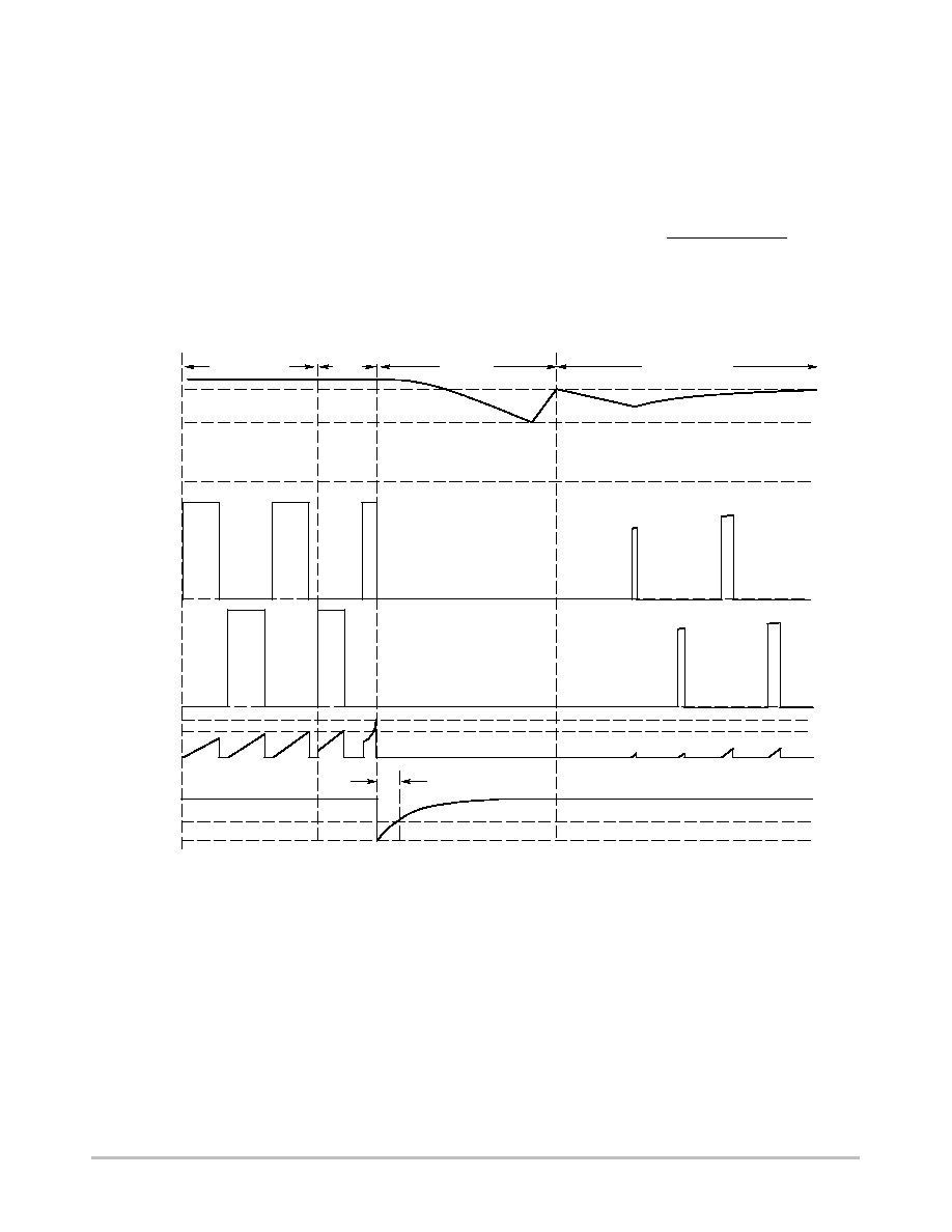
Current Limit
The NCP1561 has two overcurrent protection modes,
cycle by cycle and cycle skip. It allows the NCP1561 to
handle momentary and hard shorts differently for the best
tradeoff in system performance and safety. The outputs are
disabled typically 86 ns after a current limit fault is detected.
The cycle by cycle mode terminates the conduction cycle
(reducing the duty cycle) if the voltage on the CS pin
exceeds 0.95 V. The cycle skip mode is enabled if the voltage
on the CS pin reaches 1.15 V. Once a cycle skip fault is
detected, the outputs are disabled, the soft-start and cycle
skip capacitors are discharged, and the cycle skip period
(T
CSKIP
) commences.
The cycle skip period is set by an external capacitor
(C
CSKIP
). Once a cycle skip fault is detected, the cycle skip
capacitor is discharged followed by a charge cycle. The
charge current is 12.3
mA. The cycle skip period ends when
the voltage on the cycle skip capacitor reaches 2.0 V. If the
cycle skip period is known, the cycle skip capacitor is
calculated using the equation below:
CCSKIP
[
TCSKIP
12.3
m
A
2 V
Using the above equation, a cycle skip period of 11.0
ms
requires a cycle skip capacitor of 68 pF. The differences
between the cycle by cycle and cycle skip modes are shown
in Figure 31.
Figure 31. Overcurrent Faults Timing Diagram
Cycle Skip Voltage
0 V
0 V
0 V
0 V
0 V
OUT1
OUT2
CS Voltage
NORMAL
OPERATION
RESET
Faults
I
LIM1
I
LIM2
T
CSKIP
I
LIM
V
AUX(off)
V
AUX
V
AUX(on)
2 V
SOFT-START
Once the cycle skip period is complete and V
AUX
reaches
V
AUX(on)
, a soft-start sequence commences. The possible
minimum OFF time is set by C
CSKIP
. The actual OFF time
is generally greater than the cycle skip period if operating in
DSS because it is the cycle skip period added to the time it
takes V
AUX
to cycle between V
AUX(off)
and V
AUX(on)
. If
operating from an independent supply, the OFF time is the
cycle skip period.
Oscillator
The NCP1561 oscillator frequency is set by a single
external resistor connected between the R
T
pin and GND.
The oscillator is designed to operate up to 250 kHz.
The voltage on the R
T
pin is laser trim adjusted during
manufacturing to 1.3 V for an R
T
of 101 k
W. A current set
by R
T
generates an Oscillator Ramp by charging an internal
10 pF capacitor as shown in Figure 3. The period ends
(capacitor is discharged) once the Oscillator Ramp reaches
2.0 V. If R
T
increases, the current and the Oscillator Ramp
slope decrease, thus reducing the frequency. If R
T
decreases,
the opposite effect is obtained. Figure 17 shows the
relationship between R
T
and the oscillator frequency.

NCP1561
http://onsemi.com
16
Maximum Duty Cycle
A dedicated internal comparator limits the maximum ON
time by comparing the FF Ramp to V
DC(inv)
as shown in
Figure 3. If the FF Ramp voltage exceeds V
DC(inv)
, the
output of the Max DC Comparator goes high.
This will reset
the Output Latch, thus turning OFF the outputs and limiting
the duty cycle.
Duty cycle is defined as:
DC
+
ton
T
+
ton
f
Therefore, the maximum ON time can be set to yield the
desired DC if the operating frequency is known. The
maximum ON time is set by adjusting the FF Ramp to reach
V
DC(inv)
in a time equal to t
on(max)
as shown in Figure 32.
The maximum ON time should be set for the minimum line
voltage. As line voltage increases, the slope of the FF Ramp
increases. This reduces the duty cycle below DC
MAX
, which
is a desirable feature as the duty cycle is inversely
proportional to line voltage.
Figure 32. Maximum ON Time Limit Waveforms
Oscillator Ramp
0 V
0 V
FF Ramp
T
t
on(max)
V
DC(inv)
2 V
An internal resistor divider from a 2.0 V reference is used
to set V
DC(inv)
. If the DC
MAX
pin is grounded, V
DC(inv)
is
1.0 V. If the pin is floating, V
DC(inv)
is 1.4 V. This is
equivalent to 71% (36% DC) or 100% (50% DC) of a FF
Ramp, with a peak voltage of 1.4 V. V
DC(inv)
can be adjusted
to other values by placing an external resistor network on the
DC
MAX
pin. For example, if the minimum line voltage is 36
V, R
FF
is 432 k
W, oscillator frequency is 150 kHz and a
maximum duty cycle of 45% is required, V
DC(inv)
is
calculated as follows:
VDC(inv)
+
IFF
6.7 k
W
ton(max)
CFF
125 k
W
VDC(inv)
+
81.0
m
A
6.7 k
W
3.0
m
s
10.8 pF
125 k
W
+
1.2 V
This can be achieved by connecting a 23.44 k
W resistor
from the DC
MAX
pin to GND. The maximum duty cycle
limit can be disabled connecting a 100 k
W resistor between
the DC
MAX
and V
REF
pins.
5.0 V Reference
The NCP1561 includes a precision 5.0 V reference output.
The reference output is biased directly from V
AUX
and it can
supply up to 6 mA. Load regulation is 50 mV and line
regulation is 100 mV within the specified operating range.
It is recommended to bypass the reference output with a
0.1
mF ceramic capacitor. The reference output is disabled
when an UV fault is present.
PWM Comparator
In steady state operation, the PWM Comparator adjusts
the duty cycle by comparing the error signal to the FF Ramp
(voltage-mode) or a ramp proportional to the inductor
current (current-mode). The error signal is fed into the V
EA
input. The FF Ramp or the inductor ramp is fed into the
RAMP_IN pin. If operating in voltage-mode, the
connection between the RAMP_OUT and RAMP_IN pins
should be as close as possible to minimize parasitic
inductance. It can be easily routed underneath the package.
The V
EA
input can be driven directly with an optocoupler
and a pull up resistor (R
EA
) from V
REF
as shown in Figure
33. The drive of the control pin is simplified by internally
incorporating a series diode and resistor. The series diode
provides a 0.7 V offset between the V
EA
input and the PWM
Comparator inverting input. The outputs are enabled if the
V
EA
voltage is approximately 0.7 V above the valley voltage
of the ramp (V
valley
) in the RAMP_IN pin.
Figure 33. Optocoupler driving V
EA
input
-
+
-
+
PWM
Comparator
FF Ramp
or
Inductor Ramp
Feedback
Signal
RAMP_IN
R
EA
V
REF
V
EA
V
EA
V
peak
V
valley
20 k
W
2 k
W
0 V
12
11
10
The pull-up resistor is selected such that in the absence of
the error signal, the voltage on the V
EA
pin exceeds the peak
amplitude of the ramp in the RAMP_IN pin. Otherwise, the
converter may not be able to reach maximum duty cycle. If
operating in voltage-mode, R
EA
is calculated using the
equation below:
REA
t
22 k
W
VREF
*
0.7 V
Vvalley
)
0.0515
IFF
CFF
f
*
1
where, C
FF
is the internal FF capacitor, typically 10.8 pF.

NCP1561
http://onsemi.com
17
Soft-Start
Soft-start (SS) allows the converter to gradually reach
steady state operation, thus reducing startup stress and
surges on the system. The duty cycle is limited during a
soft-start sequence by comparing the Oscillator Ramp to the
SS voltage (V
SS
) by means of the Soft-Start Comparator.
Once faults are removed and V
AUX
reaches V
AUX(on)
, a
6.2
mA current source starts to charge the capacitor on the SS
pin. The Soft-Start Comparator controls the duty cycle
while the SS voltage is below 2.0 V. Once V
SS
reaches 2.0 V,
it exceeds the Oscillator Ramp voltage and the Soft-Start
Comparator does not limit the duty cycle. Figure 34 shows
the relationship between the outputs duty cycle and the
soft-start voltage.
Figure 34. Soft Start Timing Diagram
OUT2
OUT1
V
SS
Oscillator
Ramp
If the soft start period is too long, V
AUX
may discharge to
7 V before the converter output is completely in regulation
causing the outputs to be disabled. If the converter output is
not completely discharged when the outputs are re-enabled,
the converter will eventually reach regulation exhibiting a
non-monotonic startup behavior. But, if the converter
output is completely discharged when the outputs are
re-enabled, the cycle may repeat and the converter will not
start.
In the event of an UV or cycle skip fault, the soft-start
capacitor is discharged. Once the fault is removed, a
soft-start cycle commences. The soft-start steady state
voltage is approximately 4.1 V.
Control Outputs
The NCP1561 has two off-phase control outputs, OUT1
and OUT2. Figure 35 shows the relationship between OUT1
and OUT2.
Figure 35. Control Outputs Timing Diagram
OUT1
OUT2
Once V
AUX
reaches V
AUX(on)
, the internal startup circuit
is disabled and the One Shot Pulse Generator is enabled. If
no faults are present, the outputs turn ON. Otherwise, the
outputs remain OFF until the fault is removed and V
AUX
reaches V
AUX(on)
again.
The control outputs are biased from V
AUX
. The outputs
can supply up to 10 mA each and their high state voltage is
usually 0.2 V below V
AUX
. Therefore, the auxiliary supply
voltage should not exceed the maximum input voltage of the
driver stage.
If the control outputs need to drive a large capacitive load,
a driver should be used between the NCP1561 and the load.
Figures 19 and 20 show the relationship between the
output's rise and fall times vs capacitive load.
Thermal Protection
Internal Thermal Shutdown Circuitry is provided to
protect the integrated circuit in the event the maximum
junction temperature is exceeded. When activated, typically
at 180
_C, the controller is forced into a low power reset
state, discharging the soft-start capacitor and disabling the
output drivers and the bias regulator. Once the junction
temperature falls below 163
_C, the NCP1561 enters a
soft-start mode and it is allowed to resume normal
operation. This feature is provided to prevent catastrophic
failures from accidental device overheating.
Application Information
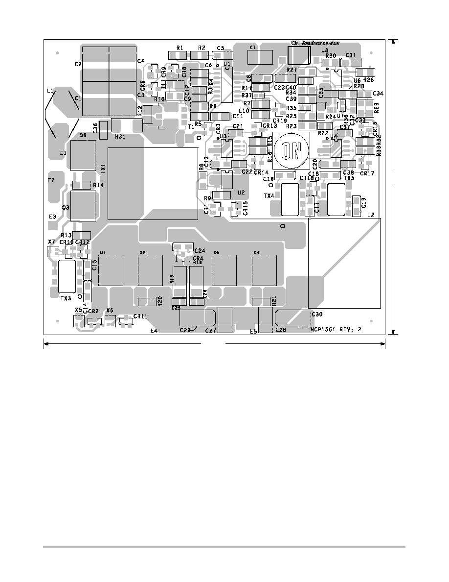
A dc-dc converter for a 48 V telecom system is designed
and implemented using the NCP1561. The converter
delivers 125 W at 2.5 V and achieves a full load efficiency
of 85%. The system is built using a 4 layer FR4, single sided
board. The converter footprint is 3.25 in x 3.75 in. The
components location within the board is shown in Figure 36
and the complete circuit schematic is shown in Figure 37.
The Bill of Material is listed in Table 1. The layout files are
available. Please contact your sales representative for more
information.
NCP1561
http://onsemi.com
18
Figure 36. Demo Board Top View
3.75"
3.25"

NCP1561
http://onsemi.com
19
Figure 37. NCP1561 Demo Board Circuit Schematic
ON/OFF
5V REF
5V REF
OU
T
B
OU
T
B
SEC_PWR
VA
U
X
SEC_PWR
R36
0
C14
CR12
BAV70
C31
0.1
C37
R27
10k
U4
8
2
3
1
4
5
6
7
N/
C
IN
_
A
GN
D
N/
C_1
IN
_
B
OU
T
_
B
VCC
OU
T
_
A
R31
6.2
R34
C33
C22 100p
CR4
BA
V70
CR1
BA
V70
C35
TX4
PULSE_P0544
C6 0.01
C28
47
TX3
PULSE_P0544
R33
R29
5.49k
CR16
R1
1M
R6
CR9
U6A
LM258
+
-
C25
R9
C36
CR1
1
C27
47
C9
R35
0
C38
Q3
SUD40N10-
25
X7
R25
+
C29
R32
C15
E1
C7
22
C8 0.1
R2
C32
C5
0.1
U1
NCP1561
4
1
3
2
16
15
13
10
8
9
7
5
11
12
6
14
VFF
Vi
n
RAM
P
_O
UT
UV
V
aux
Ou
t1
Ou
t2
Ve
a
DCm
ax
SS
RT
CS
V
ref
RAM
P
_I
N
C_Skip
GN
D
L1
R23
1.43k
CR8
R37
0
C16
0.1
R28
21.0k
Q1
C2 10
C4 10
U7
TVL431A
U3
8
2
3
1
4
5
6
7
N/
C
IN
_
A
GN
D
N/
C_1
IN
_
B
OU
T
_
B
VCC
OU
T
_
A
SFH615A-4
U8
C12
E2
LM2931
U2
8
3
4
1
7
6
2
5
Vi
n
GN
D
ADJ
V
out
GN
D
GN
D
GN
D
SD
R24
T1
PULSE_PS8202T
CR10
R8
24.9k
R5
O
PEN
C19
0.1
C40
O
PEN
CR3
Q5
CR6
R13
C1
10
L2
R4
R21
R17
29.4k
CR18
E3
R16 1.0k
Q6
SUD40N10-
25
E5
X6
C20
0.1
C17 0.1
Q2
C10
0.12
X5
R3
CR19
O
PEN
CR2
C24
0.1
C3
10
C21
CR14
CR17
U6B LM258
-
R18
6.2
R30
R26
C39
R19
6.2
E4
R7
O
PEN
C13 0.1
C1
1
0.22
R20
R1
1
6.98
R12
4T
1T
TX1
P
A
Y
T
O
N_9557
CR13
BA
V70
CR15
R22
10.0
TX5
PULSE_P0544
R15
1.0k
C23 0.1
Q4
R14
R10
+
C30
BA
V70
MMBT2907
10k
1
10N02
1
10N02
1000p
1.
0
m
H
330
330
BA
V70
1000p
1
10N02
1
10N02
BA
V70
MMBT2907
10k
VA
U
X
249k
10k
100
1000p
BA
V70
BA
V70
BA
V70
100
523k
46.4k
VA
U
X
124k
BA
V70
BA
V70
BA
V70
750
47p
BA
V70
BA
V70
BA
V70
VA
U
X
1000p
100p
47p
750
10k
6.04k
10k
MMBT2907
1000p
19.6
k
2700p
20.5k
1800p
100p
680p
21.0k
+
C26
1000p
C34
C18
0.1
2.2
m
H
3T
1T
O
PEN
2.5 V
-
+
+
36 - 72 V
-
MC33152
MC33152
0.1
0.1

NCP1561
http://onsemi.com
20
Table 1. NCP1561 Demo Board Bill of Material
Quantity
Part Reference
Part
Value
Vendor
Comments
4
C1-C4
C5750X7R1H106M
10
m
F
TDK
50 V
13
C5, C8, C13-C20, C23, C24, C31
C3216X7R2A104K
0.1
m
F
TDK
100 V
1
C6
C2012X7R1H103K
0.01
m
F
TDK
50 V
1
C7
C4532X7R1C226MT
22
m
F
TDK
16 V
5
C9, C12, C25, C26, C35
VJ0805A102KXBAT
1000 pF
Vishay (VITRAMON)
100 V
1
C10
VJ1206Y124KXXAT
0.12
m
F
Vishay (VITRAMON)
25 V
1
C11
C3216X7R1H224KT
0.22
m
F
TDK
25 V
3
C21, C22, C34
VJ0805A101KXBAT
100 pF
Vishay (VITRAMON)
100 V
2
C27, C28
C4532X5R0J476M
47
m
F
TDK
6.3 V
2
C29, C30
T495X337K006AS
330
m
F
KEMET
6 V
1
C32
VJ0805A681KXBAT
680 pF
Vishay (VITRAMON)
100 V
1
C33
VJ1206A182KXBAT
1800 pF
Vishay (VITRAMON)
100 V
1
C36
VJ1206A102KXBAT
1000 pF
Vishay (VITRAMON)
100 V
2
C37, C38
VJ0805A470KXBAT
47 pF
Vishay (VITRAMON)
100 V
1
C39
VJ1206A272KXBAT
2700 pF
Vishay (VITRAMON)
100 V
1
C40
-
OPEN
-
OPEN
16
CR1-CR4, CR6, CR8-CR18
BAV70LT1
-
ON Semiconductor
Dual Diode
1
CR19
-
OPEN
-
OPEN
1
L1
DO3316P-222
2.2
m
H
COILCRAFT
1
L2
9558
1.0
m
H
PAYTON
4
Q1, Q2, Q4, Q5
NTD110N02R
-
ON Semiconductor
24 V, N-MOSFET
2
Q3, Q6
SUD40N10-25
-
VISHAY
100 V, N-MOSFET
1
R1
CRCW12061004FRE4
1M
Vishay (DALE)
1%
2
R2, R10
CRCW1206101JRT1
100
Vishay (DALE)
5%
1
R3
CRCW12065233FRT1
523k
Vishay (DALE)
1%
1
R4
CRCW12064642FRT1
46.4k
Vishay (DALE)
1%
3
R5, R7, R34
-
OPEN
-
OPEN
1
R6
CRCW12061243FRT1
124k
Vishay (DALE)
1%
1
R9
CRCW12062493FRT1
249k
Vishay (DALE)
1%
5
R12, R13, R14, R20, R21
CRCW1206103JRT1
10k
Vishay (DALE)
5%
1
R8
CRCW12062492FRT1
24.9k
Vishay (DALE)
1%
1
R11
CRCW12066R98FRT1
6.98
Vishay (DALE)
1%
2
R15, R16
CRCW12061001FRT1
1.0k
Vishay (DALE)
1%
1
R17
CRCW12062942FRT1
29.4k
Vishay (DALE)
1%
3
R18, R19, R31
CRCW25126R19FRT1
6.2
Vishay (DALE)
5%
1
R22
CRCW080510R0FRT1
10
Vishay (DALE)
1%
1
R23
CRCW12061431FRT1
1.43k
Vishay (DALE)
1%
1
R24
CRCW12062052FRT1
20.5k
Vishay (DALE)
1%
1
R25
CRCW12061962FRT1
19.6k
Vishay (DALE)
1%
2
R26, R28
CRCW12062102FRT1
21.0k
Vishay (DALE)
1%
1
R27
CRCW1206103JRT1
10k
Vishay (DALE)
5%
1
R29
CRCW12065491FRT1
5.49k
Vishay (DALE)
1%
1
R30
CRCW12066041FRT1
6.04k
Vishay (DALE)
1%
R32, R33
CRCW12067500FRT1
750
Vishay (DALE)
1%
3
R35-R37
CRCW0603000ZT
0
Vishay (DALE)
5%
1
T1
PS8202T
-
PULSE
Current Sense Transformer
1
TX1
9557
-
PAYTON
Power Transformer
3
TX3-TX5
P0544
-
PULSE
Gate Drive Transformer
1
U1
NCP1561DR2
-
ON Semiconductor
Controller
1
U2
LM2931CD
-
ON Semiconductor
Voltage Regulator
2
U3, U4
MC33152D
-
ON Semiconductor
MOSFET Driver
1
U6
LM258D
-
ON Semiconductor
Dual OpAmp
1
U7
TVL431ASNT1
-
ON Semiconductor
Regulator
1
U8
SFH6156-4
-
VISHAY
Poptocoupler
3
X5-X7
MMBT2907AWT1
-
ON Semiconductor
PNP transistor

NCP1561
http://onsemi.com
21
PACKAGE DIMENSIONS
SO-16
D SUFFIX
CASE 751B-05
ISSUE J
NOTES:
1. DIMENSIONING AND TOLERANCING PER ANSI
Y14.5M, 1982.
2. CONTROLLING DIMENSION: MILLIMETER.
3. DIMENSIONS A AND B DO NOT INCLUDE
MOLD PROTRUSION.
4. MAXIMUM MOLD PROTRUSION 0.15 (0.006)
PER SIDE.
5. DIMENSION D DOES NOT INCLUDE DAMBAR
PROTRUSION. ALLOWABLE DAMBAR
PROTRUSION SHALL BE 0.127 (0.005) TOTAL
IN EXCESS OF THE D DIMENSION AT
MAXIMUM MATERIAL CONDITION.
1
8
16
9
SEATING
PLANE
F
J
M
R
X 45
_
G
8 PL
P
-B-
-A-
M
0.25 (0.010)
B
S
-T-
D
K
C
16 PL
S
B
M
0.25 (0.010)
A
S
T
DIM
MIN
MAX
MIN
MAX
INCHES
MILLIMETERS
A
9.80
10.00
0.386
0.393
B
3.80
4.00
0.150
0.157
C
1.35
1.75
0.054
0.068
D
0.35
0.49
0.014
0.019
F
0.40
1.25
0.016
0.049
G
1.27 BSC
0.050 BSC
J
0.19
0.25
0.008
0.009
K
0.10
0.25
0.004
0.009
M
0
7
0
7
P
5.80
6.20
0.229
0.244
R
0.25
0.50
0.010
0.019
_
_
_
_

NCP1561
http://onsemi.com
22
ON Semiconductor and are registered trademarks of Semiconductor Components Industries, LLC (SCILLC). SCILLC reserves the right to make changes without further notice
to any products herein. SCILLC makes no warranty, representation or guarantee regarding the suitability of its products for any particular purpose, nor does SCILLC assume any liability
arising out of the application or use of any product or circuit, and specifically disclaims any and all liability, including without limitation special, consequential or incidental damages.
"Typical" parameters which may be provided in SCILLC data sheets and/or specifications can and do vary in different applications and actual performance may vary over time. All
operating parameters, including "Typicals" must be validated for each customer application by customer's technical experts. SCILLC does not convey any license under its patent rights
nor the rights of others. SCILLC products are not designed, intended, or authorized for use as components in systems intended for surgical implant into the body, or other applications
intended to support or sustain life, or for any other application in which the failure of the SCILLC product could create a situation where personal injury or death may occur. Should
Buyer purchase or use SCILLC products for any such unintended or unauthorized application, Buyer shall indemnify and hold SCILLC and its officers, employees, subsidiaries, affiliates,
and distributors harmless against all claims, costs, damages, and expenses, and reasonable attorney fees arising out of, directly or indirectly, any claim of personal injury or death
associated with such unintended or unauthorized use, even if such claim alleges that SCILLC was negligent regarding the design or manufacture of the part. SCILLC is an Equal
Opportunity/Affirmative Action Employer. This literature is subject to all applicable copyright laws and is not for resale in any manner.
PUBLICATION ORDERING INFORMATION
N. American Technical Support: 800-282-9855 Toll Free
USA/Canada
Japan: ON Semiconductor, Japan Customer Focus Center
2-9-1 Kamimeguro, Meguro-ku, Tokyo, Japan 153-0051
Phone: 81-3-5773-3850
NCP1561/D
The product described herein (NCP1561) may be covered by one or more U.S. patents. There may be other patents pending.
LITERATURE FULFILLMENT:
Literature Distribution Center for ON Semiconductor
P.O. Box 61312, Phoenix, Arizona 85082-1312 USA
Phone: 480-829-7710 or 800-344-3860 Toll Free USA/Canada
Fax: 480-829-7709 or 800-344-3867 Toll Free USA/Canada
Email: orderlit@onsemi.com
ON Semiconductor Website: http://onsemi.com
Order Literature: http://www.onsemi.com/litorder
For additional information, please contact your
local Sales Representative.