 | ÐлекÑÑоннÑй компоненÑ: NCP1582 | СкаÑаÑÑ:  PDF PDF  ZIP ZIP |
NCP1582
©
Semiconductor Components Industries, LLC, 2006
April, 2006 - Rev. 1
1
Publication Order Number:
NCP1582/D
NCP1582, NCP1582A,
NCP1583
Low Voltage Synchronous
Buck Controllers
The NCP158x is a low cost PWM controller designed to operate from
a 5 V or 12 V supply. This device is capable of producing an output
voltage as low as 0.8 V. This 8-pin device provides an optimal level of
integration to reduce size and cost of the power supply. Features include a
0.7 A gate driver and an internally set 350 kHz (NCP1582, NCP1582A)
and a 300 kHz (NCP1583) oscillator. The NCP158x also incorporates an
externally compensated transconductance error amplifier and a
programmable soft-start function. Protection features include short
circuit protection (SCP) and under voltage lockout (UVLO). The
NCP158x comes in an 8-pin SOIC package.
Features
·
Input Voltage Range from 4.5 V to 13.2 V
·
350 kHz (NCP1582, NCP1582A), 300 kHz (NCP1583) Internal
Oscillator
·
Boost Pin Operates to 30 V
·
Voltage Mode PWM Control
·
0.8 V
$1.5% Internal Reference Voltage
·
Adjustable Output Voltage
·
Programmable Soft-Start
·
Internal 0.7 A Gate Drivers
·
80% Max Duty Cycle
·
Input UVLO
·
R
DS(on)
Current Sensing for Short Circuit Protection
·
These are Pb-Free Devices
Applications
·
Graphics Cards
·
Desktop Computers
·
Servers/Networking
·
DSP and FPGA Power Supply
·
DC-DC Regulator Modules
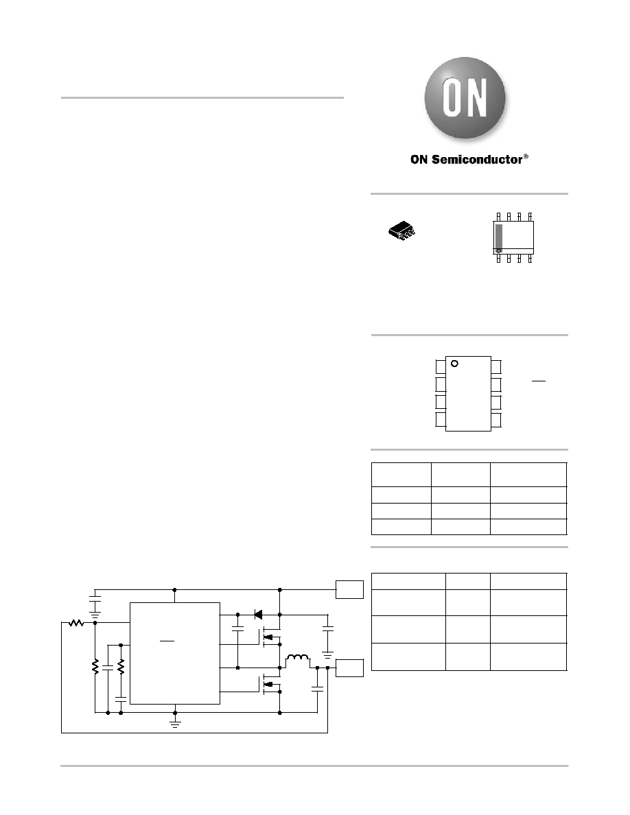
BST
TG
GND
BG
COMP/DIS
FB
V
CC
V
IN
V
OUT
Figure 1. Typical Application Diagram
PHASE
SOIC-8
D SUFFIX
CASE 751
1
8
MARKING DIAGRAM
PIN CONNECTIONS
x
= 2, 2A or 3
A
= Assembly Location
L
= Wafer Lot
Y
= Year
W
= Work Week
G
= Pb-Free Device
1
BST
8 PHASE
2
TG
3
GND
4
BG
7 COMP/DIS
6 FB
5 V
CC
(Top View)
158x
ALYW
G
Device
Package
Shipping
ORDERING INFORMATION
NCP1582DR2G
SOIC-8
(Pb-Free)
2500/Tape & Reel
For information on tape and reel specifications,
including part orientation and tape sizes, please
refer to our Tape and Reel Packaging Specifications
Brochure, BRD8011/D.
1
8
http://onsemi.com
NCP1582ADR2G
SOIC-8
(Pb-Free)
2500/Tape & Reel
NCP1583DR2G
SOIC-8
(Pb-Free)
2500/Tape & Reel
NCP158x
Series
Oscillator
Frequency
SCP Trip Voltage
NCP1582
350 kHz
-350 mV
NCP1582A
350 kHz
-450 mV
NCP1583
300 kHz
-350 mV
NCP1582, NCP1582A, NCP1583
http://onsemi.com
2
Figure 2. Typical VGA Card Application Diagram
BST
TG
GND
BG
COMP/DIS
FB
V
CC
V
OUT
PHASE
12 V
3.3 V
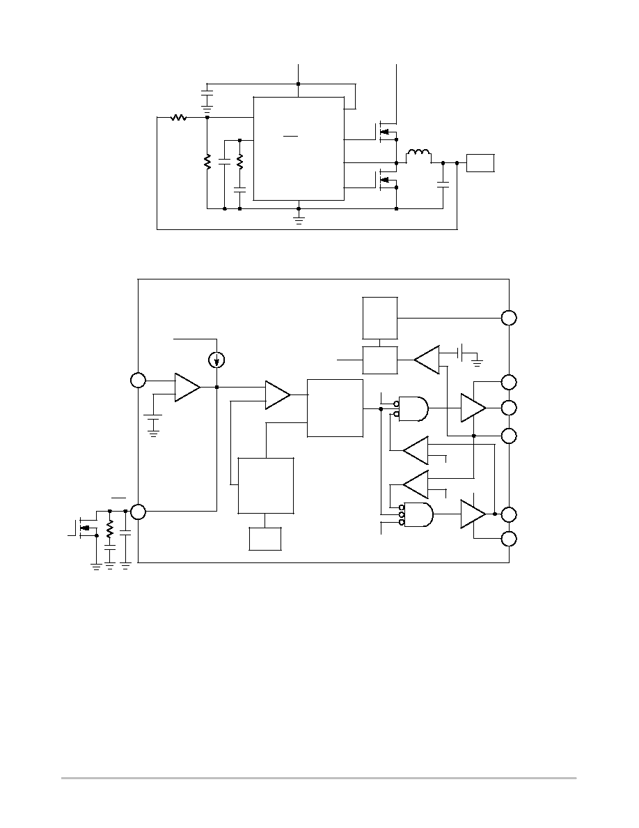
Figure 3. Detailed Block Diagram
LATCH
FB
COMP/DIS
0.8 V
(V
REF
)
V
CC
+
-
Clock
Ramp
OSC
OSC
R
S
Q
PWM
OUT
FAULT
+
-
2 V
+
-
2 V
FAULT
TG
BST
PHASE
V
CC
BG
GND
7
1
2
8
4
3
FAULT
+
-
SCP
POR
UVLO
5
+
-
6
SCP Trip Voltage
NCP1582, NCP1582A, NCP1583
http://onsemi.com
3
PIN FUNCTION DESCRIPTION
Pin No.
Symbol
Description
1
BST
Supply rail for the floating top gate driver. To form a boost circuit, use an external diode to bring the
desired input voltage to this pin (cathode connected to BST pin). Connect a capacitor (C
BST
) between this pin
and the PHASE pin. Typical values for C
BST
range from 0.1
m
F to 1
m
F. Ensure that C
BST
is placed near the IC.
2
TG
Top gate MOSFET driver pin. Connect this pin to the gate of the top N-Channel MOSFET.
3
GND
IC ground reference. All control circuits are referenced to this pin.
4
BG
Bottom gate MOSFET driver pin. Connect this pin to the gate of the bottom N-Channel MOSFET.
5
V
CC
Supply rail for the internal circuitry. Operating supply range is 4.5 V to 15 V. Decouple with a 1
m
F
capacitor to GND. Ensure that this decoupling capacitor is placed near the IC.
6
FB
This pin is the inverting input to the error amplifier. Use this pin in conjunction with the COMP pin to
compensate the voltage-control feedback loop. Connect this pin to the output resistor divider (if used) or
directly to Vout.
7
COMP/DIS
Compensation Pin. This is the output of the error amplifier (EA) and the non-inverting input of the PWM
comparator. Use this pin in conjunction with the FB pin to compensate the voltage-control feedback loop. The
compensation capacitor also acts as a soft-start capacitor. Pull this pin low with an open drain transistor for
disable.
8
PHASE
Switch node pin. This is the reference for the floating top gate driver. Connect this pin to the source of the top
MOSFET.
ABSOLUTE MAXIMUM RATINGS
Pin Name
Symbol
V
MAX
V
MIN
Main Supply Voltage Input
V
CC
15 V
-0.3 V
Bootstrap Supply Voltage Input
BST
30 V wrt/GND
15 V wrt/PHASE
-0.3 V
Switching Node (Bootstrap Supply Return)
PHASE
24 V
-0.7 V
-5.0 V for < 50 ns
High-Side Driver Output (Top Gate)
TG
30 V wrt/GND
15 V wrt/PHASE
-0.3 V
wrt/PHASE
Low-Side Driver Output (Bottom Gate)
BG
15 V
-0.3 V
Feedback
FB
5.5 V
-0.3 V
COMP/DISABLE
COMP/DIS
5.5 V
-0.3 V
MAXIMUM RATINGS
Rating
Symbol
Value
Unit
Thermal Resistance, Junction-to-Ambient
R
q
JA
165
°
C/W
Thermal Resistance, Junction-to-Case
R
q
JC
45
°
C/W
Operating Junction Temperature Range
T
J
-40 to 150
°
C
Operating Ambient Temperature Range
T
A
-40 to 85
°
C
Storage Temperature Range
T
stg
-55 to +150
°
C
Lead Temperature Soldering (10 sec): Reflow (SMD styles only) Pb-Free
(Note 1)
260 peak
°
C
Moisture Sensitivity Level
MSL
1
-
Stresses exceeding Maximum Ratings may damage the device. Maximum Ratings are stress ratings only. Functional operation above the
Recommended Operating Conditions is not implied. Extended exposure to stresses above the Recommended Operating Conditions may affect
device reliability.
1. 60-180 seconds minimum above 237
°
C.
NCP1582, NCP1582A, NCP1583
http://onsemi.com
4
ELECTRICAL CHARACTERISTICS
(0
_
C < T
A
< 70
_
C, -40
_
C < T
J
< 125
_
C (Note 2), 4.5 V < V
CC
< 13.2 V, 4.5 V < BST < 26.5 V,
C
TG
= C
BG
= 1.0 nF(REF:NTD30N02), for min/max values unless otherwise noted.)
Characteristic
Conditions
Min
Typ
Max
Unit
Input Voltage Range
4.5
13.2
V
Boost Voltage Range
4.5
26.5
V
Supply Current
Quiescent Supply Current
V
FB
= 1.0 V, No Switching
V
CC
= 13.2 V
-
1.0
1.75
mA
Boost Quiescent Current
V
FB
= 1.0 V, No Switching
-
140
-
m
A
Under Voltage Lockout
UVLO Threshold
V
CC
Rising Edge
3.85
4.2
V
UVLO Hysteresis
-
0.5
V
Switching Regulator
VFB Feedback Voltage,
Control Loop in Regulation
T
A
= 0 to 70
°
C
-40 to 125
°
C
0.788
0.8
0.8
0.812
V
Oscillator Frequency (NCP1582,
NCP1582A)
T
A
= 0 to 70
°
C
-40 to 125
°
C
300
350
350
400
kHz
Oscillator Frequency (NCP1583)
T
A
= 0 to 70
°
C
-40 to 125
°
C
275
300
300
325
kHz
Ramp-Amplitude Voltage
-
1.1
-
V
Minimum Duty Cycle
-
0
-
%
Maximum Duty Cycle
70
75
80
%
Minimum Pulse Width
Static Operating
100
150
ns
Blanking Time
50
ns
BG Minimum On Time
~500
ns
Error Amplifier (GM)
Transconductance
5.0
mmho
Open Loop DC Gain
55
70
-
DB
Output Source Current
Output Sink Current
V
FB
= 0.8 V
V
FB
> 0.8 V
80
80
120
120
m
A
m
A
Input Offset Voltage
-2.0
0
2.0
mV
Input Bias Current
0.1
1.0
m
A
Unity Gain Bandwidth
4.0
Mhz
Soft-Start
SS Source Current
V
FB
< 0.8 V
5.0
10
15
m
A
Switch Over Threshold
100
% of Vref
Current Limit
Trip Voltage (NCP1582, NCP1583)
Vphase to ground
-350
mV
Trip Voltage (NCP1582A)
Vphase to ground
-450
mV
Gate Drivers
Upper Gate Source
Vgs = 6.0 V
-
0.7
A
Upper Gate Sink
Vugate wrt Phase = 1.0 V
2.4
W
Lower Gate Source
Vgs = 6.0 V
-
0.7
A
Lower Gate Sink
Vlgate wrt GND = 1.0 V
2.2
W
PHASE Falling to BG Rising Delay
V
CC
= 12 V, PHASE < 2.0 V, BG > 2.0 V
-
30
90
ns
BG Falling to TG Rising Delay
V
CC
= 12 V, BG < 2.0 V, TG > 2.0 V
-
30
60
ns
Enable Threshold
0.4
V
2. Specifications to -40
°
C are guaranteed via correlation using standard quality control (SQC), not tested in production.
NCP1582, NCP1582A, NCP1583
http://onsemi.com
5
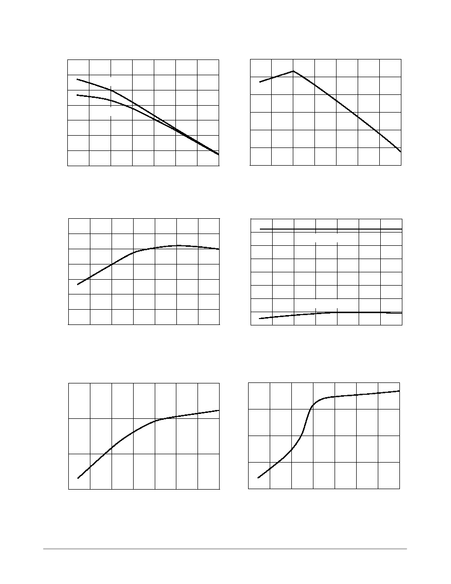
TYPICAL OPERATING CHARACTERISTICS
4.2
4.1
4.0
3.9
3.8
4.3
-50
-25
0
25
50
75
100
125
T
J
, JUNCTION TEMPERATURE (
°
C)
I
CC
,
SUPPL
Y CURRENT (mA)
380
-50
-25
0
25
50
75
100
125
T
J
, JUNCTION TEMPERATURE (
°
C)
F
SW
, FREQUENCY (kHz)
370
360
350
340
330
320
310
Figure 4. Oscillator Frequency (F
SW
) vs.
Temperature
Figure 5. I
CC
vs. Temperature
3.7
808
804
800
796
792
788
784
812
-50
-25
0
25
50
75
100
125
T
J
, JUNCTION TEMPERATURE (
°
C)
V
ref
, REFERENCE VOL
T
AGE (mV)
4.4
-50
-25
0
25
50
75
100
125
T
J
, JUNCTION TEMPERATURE (
°
C)
UVLO RISING/F
ALLING
(V)
4.3
4.2
4.1
4.0
3.9
3.6
-50
-25
0
25
50
75
100
125
T
J
, JUNCTION TEMPERATURE (
°
C)
SOFT
ST
AR
T SOURCING CURRENT (
m
A)
12
11
10
9.0
Figure 6. Reference Voltage (V
ref
) vs. Temperature
Figure 7. UVLO vs. Temperature
Figure 8. Soft Start Sourcing Current vs.
Temperature
Figure 9. I-Limit vs. Temperature
3.7
3.8
V
CC
= 5.0 V
V
CC
= 12 V
T
J
, JUNCTION TEMPERATURE (
°
C)
I-LIMIT TRIP (mV)
500
-50
-25
0
25
50
75
100
125
450
400
300
350
RISING
FALLING
NCP1582, NCP1582A, NCP1583
http://onsemi.com
6
DETAILED OPERATING DESCRIPTION
General
The NCP158x is an 8-pin PWM controller intended for
DC-DC conversion from 5.0 V & 12 V buses. The NCP158x
has a 0.7 A internal gate driver circuit designed to drive
N-channel MOSFETs in a synchronous-rectifier buck
topology. The output voltage of the converter can be
precisely regulated down to 800 mV 1.5% when the V
FB
pin
is tied to V
OUT
. The switching frequency is internally set. A
high gain operational transconductance error amplifier
(OTA) is used.
Duty Cycle and Maximum Pulse Width Limits
In steady state DC operation, the duty cycle will stabilize
at an operating point defined by the ratio of the input to the
output voltage. The NCP158x can achieve an 80% duty
cycle. There is a built in off-time which ensures that the
bootstrap supply is charged every cycle. The NCP158x,
which is capable of a 100 nsec pulse width (min.), can allow
a 12 V to 0.8 V conversion at 350 kHz.
Input Voltage Range (V
CC
and BST)
The input voltage range for both V
CC
and BST is 4.5 V to
13.2 V with respect to GND and PHASE, respectively.
Although BST is rated at 13.2 V with respect to PHASE, it
can also tolerate 26.5 V with respect to GND.
External Enable/Disable
When the Comp pin voltage falls or is pulled externally
below the 400 mv threshold, it disables the PWM Logic and
the gate drive outputs. In this disabled mode, the operational
transconductance error amplifier's (EOTA) output source
current is reduced and limited to the Soft Start current of 10
mA.
Normal Shutdown Behavior
Normal shutdown occurs when the IC stops switching
because the input supply reaches UVLO threshold. In this
case, switching stops, the internal SS is discharged, and all
GATE pins go low. The switch node enters a high impedance
state and the output capacitors discharge through the load
with no ringing on the output voltage.
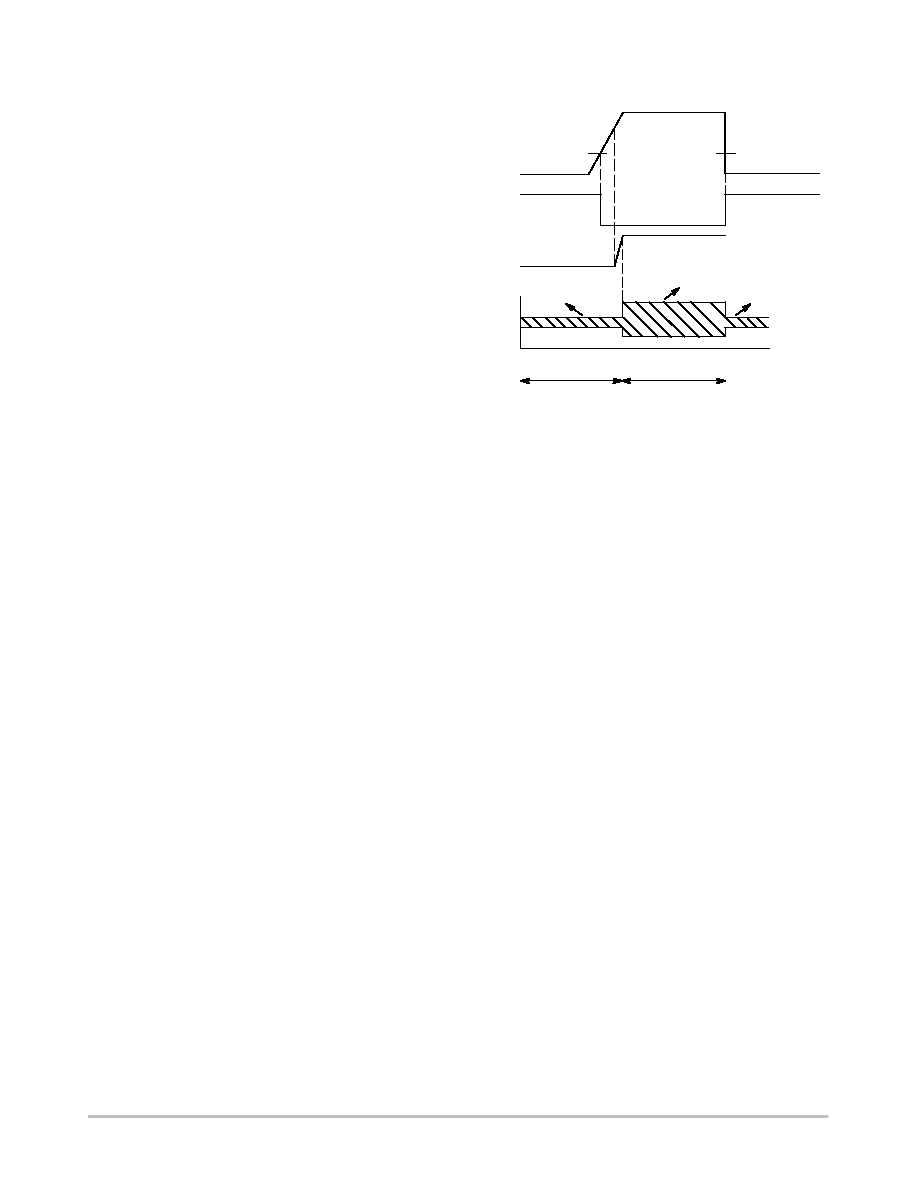
External Soft Start
The NCP158x features an external soft start function,
which reduces inrush current and overshoot of the output
voltage. Soft start is achieved by using the internal current
source of 10
mA. (typ), which charges the external integrator
capacitor of the transconductance amplifier. Figure 10 is a
typical soft start sequence. This sequence begins once V
CC
surpasses its UVLO threshold. During Soft Start, as the
Comp Pin rises through 400 mV, the PWM Logic and gate
drives are enabled. When the feedback voltage crosses
800 mV, the EOTA will be given control to switch to its
higher regulation mode output current of 120
mA. In the
event of an overcurrent during soft start, the overcurrent
logic will override the soft start sequence and will shut down
the PWM logic and both the high side and low side gates.
Figure 10. Soft Start Implementation
0.4 V
1.1 V
0.4 V
V
comp
Enable
V
fb
10 mA
10 mA
120 mA
Isource/
Sink
SS
-10 mA
Start Up
Normal
Timing Diagram NCP1582: Enable Sequence
UVLO
Under Voltage Lockout (UVLO) is provided to ensure that
unexpected behavior does not occur when V
CC
is too low to
support the internal rails and power the converter. For the
NCP158x, the UVLO is set to ensure that the IC will start up
when V
CC
reaches 4.2 V and shutdown when V
CC
drops
below 3.7 V. This permits operation when converting from
a 5.0 input voltage.
Current Limit Protection
In case of a short circuit or overload, the low-side (LS)
FET will conduct large currents. The controller will shut
down the regulator in this situation for protection against
overcurrent. The low-side R
DSon
sense is implemented by
comparing the voltage at the Phase node when BG starts
going low to an internally generated fixed voltage. If the
phase voltage is lower than SCP trip voltage, an overcurrent
condition occurs and a counter is initiated. When the counter
completes, the PWM logic and both HS-FET and LS-FET
are turned off. The controller will retry to see if the short
circuit or overload condition is removed through the soft
start cycle. The minimum turn-on time of the LS-FET is set
to be 500 ns. The trip thresholds have a -95 mV, +45 mV
process and temperature variation.
Drivers
The NCP158x includes 0.7 A gate drivers to switch
external N-channel MOSFETs. This allows the NCP158x to
address high-power as well as low-power conversion
requirements. The gate drivers also include adaptive
non-overlap circuitry. The non-overlap circuitry increase
efficiency, which minimizes power dissipation, by
minimizing the body diode conduction time.
A detailed block diagram of the non-overlap and gate
drive circuitry used in the chip is shown in Figure 11.
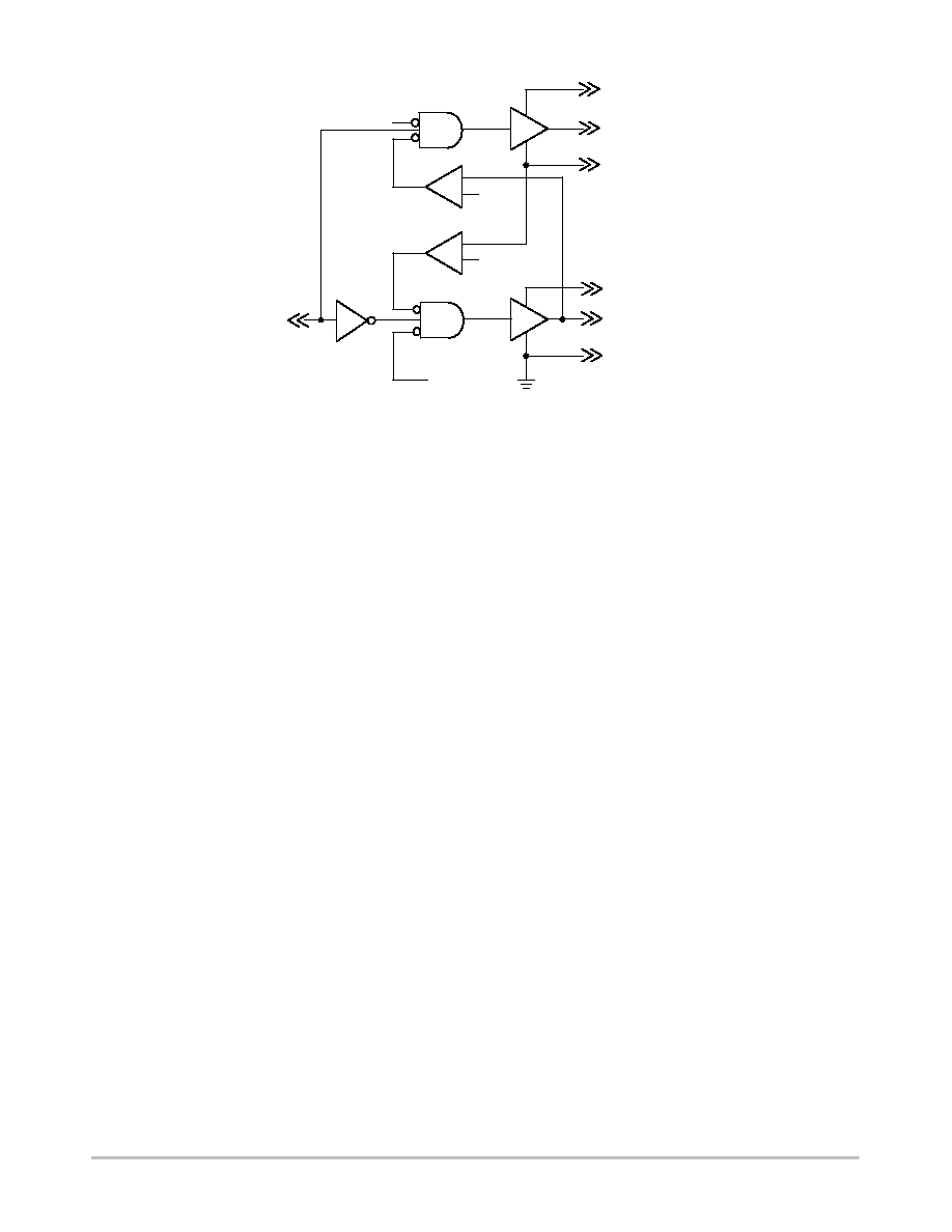
NCP1582, NCP1582A, NCP1583
http://onsemi.com
7
Figure 11. Block Diagram of Gate Driver
and Non-Overlap Circuitry
UVLO
FAULT
+
-
2 V
+
-
2 V
PHASE
TG
BST
V
CC
BG
GND
UVLO
FAULT
PWM
OUT
Careful selection and layout of external components is
required, to realize the full benefit of the onboard drivers.
The capacitors between V
CC
and GND and between BST
and SWN must be placed as close as possible to the IC. The
current paths for the TG and BG connections must be
optimized. A ground plane should be placed on the closest
layer for return currents to GND in order to reduce loop area
and inductance in the gate drive circuit.

NCP1582, NCP1582A, NCP1583
http://onsemi.com
8
APPLICATION SECTION
Input Capacitor Selection
The input capacitor has to sustain the ripple current
produced during the on time of the upper MOSFET, so it
must have a low ESR to minimize the losses. The RMS value
of this ripple is:
IinRMS
+
IOUT D
(1
*
D) ,
where D is the duty cycle, Iin
RMS
is the input RMS current,
& I
OUT
is the load current. The equation reaches its
maximum value with D = 0.5. Losses in the input capacitors
can be calculated with the following equation:
PCIN
+
ESRCIN
IinRMS
2
,
where P
CIN
is the power loose in the input capacitors &
ESR
CIN
is the effective series resistance of the input
capacitance. Due to large d
I
/d
t
through the input capacitors,
electrolytic or ceramics should be used. If a tantalum must
be used, it must be surge protected. Otherwise, capacitor
failure could occur.
Calculating Input Start-up Current
To calculate the input start up current, the following
equation can be used.
Iinrush
+
COUT
VOUT
tSS
,
where I
inrush
is the input current during start-up, C
OUT
is the
total output capacitance, V
OUT
is the desired output voltage,
and t
SS
is the soft start interval.
If the inrush current is higher than the steady state input
current during max load, then the input fuse should be rated
accordingly, if one is used.
Calculating Soft Start Time
To calculate the soft start time, the following equation can
be used.
tSS
+
(CP
)
CC) *
D
V
ISS
Where C
C
is the compensation as well as the soft start
capacitor,
C
P
is the additional capacitor that forms the second pole.
I
SS
is the soft start current
DV is the comp voltage from zero to until it reaches
regulation.
V
comp
V
out
1.1 V
D
V
The above calculation includes the delay from comp
rising to when output voltage becomes valid.
To calculate the time of output voltage rising to when it
reaches regulation;
DV is the difference between the comp
voltage reaching regulation and 1.1 V.
Output Capacitor Selection
The output capacitor is a basic component for the fast
response of the power supply. In fact, during load transient,
for the first few microseconds it supplies the current to the
load. The controller immediately recognizes the load
transient and sets the duty cycle to maximum, but the current
slope is limited by the inductor value.
During a load step transient the output voltage initial
drops due to the current variation inside the capacitor and the
ESR. (neglecting the effect of the effective series inductance
(ESL)):
D
VOUT-ESR
+ D
IOUT
ESRCOUT,
where V
OUT-ESR
is the voltage deviation of V
OUT
due to the
effects of ESR and the ESR
COUT
is the total effective series
resistance of the output capacitors.
A minimum capacitor value is required to sustain the
current during the load transient without discharging it. The
voltage drop due to output capacitor discharge is given by
the following equation:
D
VOUT-DISCHARGE
+
D
IOUT
2
LOUT
2
COUT
(VIN
D
*
VOUT)
,
where V
OUT-DISCHARGE
is the voltage deviation of V
OUT
due to the effects of discharge, L
OUT
is the output inductor
value & V
IN
is the input voltage.
It should be noted that
V
OUT-DISCHARGE
and V
OUT-ESR
are out of phase with each other, and the larger of these two
voltages will determine the maximum deviation of the
output voltage (neglecting the effect of the ESL).
Inductor Selection
Both mechanical and electrical considerations influence
the selection of an output inductor. From a mechanical
perspective, smaller inductor values generally correspond to
smaller physical size. Since the inductor is often one of the
largest components in the regulation system, a minimum
inductor value is particularly important in
space-constrained applications. From an electrical
perspective, the maximum current slew rate through the
output inductor for a buck regulator is given by:
SlewRateLOUT
+
VIN
*
VOUT
LOUT
.
This equation implies that larger inductor values limit the
regulator's ability to slew current through the output
inductor in response to output load transients. Consequently,
output capacitors must supply the load current until the
inductor current reaches the output load current level. This
NCP1582, NCP1582A, NCP1583
http://onsemi.com
9
results in larger values of output capacitance to maintain
tight output voltage regulation. In contrast, smaller values of
inductance increase the regulator's maximum achievable
slew rate and decrease the necessary capacitance, at the
expense of higher ripple current. The peak-to-peak ripple
current is given by the following equation:
Ipk
*
pkLOUT
+
VOUT(1
*
D)
LOUT
350 kHz
,
where Ipk-pk
LOUT
is the peak to peak current of the output.
From this equation it is clear that the ripple current increases
as L
OUT
decreases, emphasizing the trade-off between
dynamic response and ripple current.
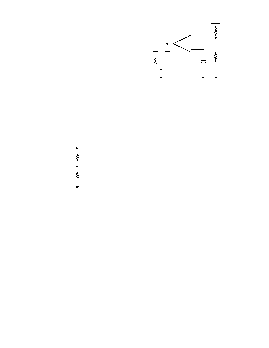
Feedback and Compensation
The NCP158x allows the output of the DC-DC converter
to be adjusted from 0.8 V to 5.0 V via an external resistor
divider network. The controller will try to maintain 0.8 V at
the feedback pin. Thus, if a resistor divider circuit was
placed across the feedback pin to V
OUT
, the controller will
regulate the output voltage proportional to the resistor
divider network in order to maintain 0.8 V at the FB pin.
V
OUT
R1
R2
FB
The relationship between the resistor divider network
above and the output voltage is shown in the following
equation:
R2
+
R1
VREF
VOUT
*
VREF
.
Resistor R1 is selected based on a design tradeoff between
efficiency and output voltage accuracy. For high values of
R1 there is less current consumption in the feedback
network, However the trade off is output voltage accuracy
due to the bias current in the error amplifier. The output
voltage error of this bias current can be estimated using the
following equation (neglecting resistor tolerance):
Error%
+
0.1
m
A
R1
VREF
100%.
Once R1 has been determined, R2 can be calculated.
Figure 12. Type II Transconductance Error
Amplifier
R1
R2
+
V
REF
EA
Gm
R
C
C
C
C
P
Figure 12 shows a typical Type II transconductance error
amplifier (EOTA). The compensation network consists of
the internal error amplifier and the impedance networks ZIN
(R
1
, R
2
) and external Z
FB
(R
c
, C
c
and C
p
). The
compensation network has to provide a closed loop transfer
function with the highest 0 dB crossing frequency to have
fast response (but always lower than F
SW
/8) and the highest
gain in DC conditions to minimize the load regulation. A
stable control loop has a gain crossing with -20 dB/decade
slope and a phase margin greater than 45
°. Include
worst-case component variations when determining phase
margin. Loop stability is defined by the compensation
network around the EOTA, the output capacitor, output
inductor and the output divider. Figure 13. shows the open
loop and closed loop gain plots.
Compensation Network Frequency:
The inductor and capacitor form a double pole at the
frequency
FLC
+
1
2
p @
LO
@
CO
The ESR of the output capacitor creates a "zero" at the
frequency,
FESR
+
1
2
p @
ESR
@
CO
The zero of the compensation network is formed as,
FZ
+
1
2
p @
RCCC
The pole of the compensation network is calculated as,
FP
+
1
2
p @
RC
@
CP
NCP1582, NCP1582A, NCP1583
http://onsemi.com
10
Figure 13. Gain Plot of the Error Amplifier
GAIN
(dB)
FREQUENCY (Hz)
100
1000
10 k
100 k
1000 k
Open Loop, Unloaded Gain
Closed Loop,
Unloaded Gain
Error Amplifier
Compensation Network
A
Gain = GMR
1
B
F
Z
F
P
Thermal Considerations
The power dissipation of the NCP158x varies with the
MOSFETs used, V
CC
, and the boost voltage (V
BST
). The
average MOSFET gate current typically dominates the
control IC power dissipation. The IC power dissipation is
determined by the formula:
PIC
+
(ICC
@
VCC)
)
PTG
)
PBG.
Where:
P
IC
= control IC power dissipation,
I
CC
= IC measured supply current,
V
CC
= IC supply voltage,
P
TG
= top gate driver losses,
P
BG
= bottom gate driver losses.
The upper (switching) MOSFET gate driver losses are:
PTG
+
QTG
@
fSW
@
VBST.
Where:
Q
TG
= total upper MOSFET gate charge at V
BST
,
f
SW
= the switching frequency,
V
BST
= the BST pin voltage.
The lower (synchronous) MOSFET gate driver losses are:
PBG
+
QBG
@
fSW
@
VCC.
Where:
Q
BG
= total lower MOSFET gate charge at V
CC
.
The junction temperature of the control IC can then be
calculated as:
TJ
+
TA
)
PIC
@ q
JA.
Where:
T
J
= the junction temperature of the IC,
T
A
= the ambient temperature,
JA
= the junction-to-ambient thermal resistance of the
IC package.
The package thermal resistance can be obtained from the
specifications section of this data sheet and a calculation can
be made to determine the IC junction temperature. However,
it should be noted that the physical layout of the board, the
proximity of other heat sources such as MOSFETs and
inductors, and the amount of metal connected to the IC,
impact the temperature of the device. Use these calculations
as a guide, but measurements should be taken in the actual
application.
Layout Considerations
As in any high frequency switching converter, layout is
very important. Switching current from one power device to
another can generate voltage transients across the
impedances of the interconnecting bond wires and circuit
traces. These interconnecting impedances should be
minimized by using wide, short printed circuit traces. The
critical components should be located as close together as
possible using ground plane construction or single point
grounding. The figure below shows the critical power
components of the converter. To minimize the voltage
overshoot the interconnecting wires indicated by heavy lines
should be part of ground or power plane in a printed circuit
board. The components shown in the figure below should be
located as close together as possible. Please note that the
capacitors C
IN
and C
OUT
each represent numerous physical
capacitors. It is desirable to locate the NCP158x within 1
inch of the MOSFETs, Q1 and Q2. The circuit traces for the
MOSFETs' gate and source connections from the NCP158x
must be sized to handle up to 2 A peak current.
Figure 14. Components to be Considered for
Layout Specifications
PHASE
TG
GND
BG
V
in
RETURN
C
in
L
C
A
D
C
out
V
out
L
out
NCP1582
NCP1582, NCP1582A, NCP1583
http://onsemi.com
11
Design Example
Switching Frequency F
SW
= 350 KHZ
Output Capacitance C
ESR
= 45 m
W/Each
Output Capacitance C
out
= 6630
mF
Output Inductance L
out
= 0.75
mH
Input Voltage V
in
= 12 V
Output Voltage V
out
= 3.3 V
Choose the loop gain crossover frequency;
FCO
+
1
10
* FSW
+
35 kHz
The corner frequency of the output filter is calculated
below;
FLC
+
1
2 *
p
* 0.75
m
H * 6630
m
F
+
2.3 kHz
Let R
C
= 1500
Check that the ESR zero frequency is not too high;
FESR
+
1
2 *
p @
CESR
@
CO
t
FSW
5
This condition is mandatory for loop stability.
Zero of the compensation network is calculated as
follows;
FZ
+
FLC
CC
+
1
2 *
p
* FZ * RC
+
1
2 *
p
* 2.3 kHz * 1500
+
46 nF
The compensation capacitor also acts as the soft start
capacitor. By adjusting the value of this compensation
capacitor, the soft start time can be adjusted.
Pole of the compensation network is calculated as
follows;
FP
+
5 * FCO
+
175 kHz
CP
+
1
2 *
p
* FP * RC
+
1
2 *
p
* 175 kHz * 1500
+
700 pF
The recommended compensation values are;
R
C
= 1500, C
C
= 46 nF, C
P
= 700 pF
The NCP158x bode plot as measured from the network
analyzer is shown below.
Figure 15. Typical Bode plot of the Open-loop
Frequency Response of the NCP158x
Top plot: Phase-Frequency (Phase Margin = 62.519
°
)
Bottom plot: Gain-Frequency (UGBW= 5 MHz)
NCP1582, NCP1582A, NCP1583
http://onsemi.com
12
Demo Board PCB Layout
SWITCH_NODE
TP1
R6
0.0
TP9
C1
L1
MH1
TP2
C12
C9
100 pF
R1
402
R8
OPEN
TP7
R4 OPEN
C10
TP3
CR1
BAS1
16L
T1
1
3
TG
MH2
TP5
MH3
C21
C1
1
R3
1.02 k
Q1
40N03
1
4
R2
OPEN
C16
Q2
40N03
1
4
3
MH4
C20 OPEN
BST
U1
NCP1582
1
7
64
8
3
2
5
COMP
FB
BG
PHASE
GND
VCC
R7
0.0
C8
1500
m
F
+12_V
IN
+
C2
1500
m
F
+
C3
1500
m
F
+
0.022
m
F
+
+
1
m
F
C4
1500
m
F
+
C5
22
m
F
+
C6
22
m
F
+
C7
22
m
F
+
TP4
0.1
m
F
1.0
m
H
TP8
3
OPEN
+
1800
m
F
C13
+
1800
m
F
C14
+
1800
m
F
C15
+
1800
m
F
10
m
F
TP6
C17
10
m
F
C18
10
m
F
C19
10
m
F
+

NCP1582, NCP1582A, NCP1583
http://onsemi.com
13
Bill of Materials
Item Number
Part Reference
Value
Quantity
MFG
1
C1 C2 C3 C4
1500
m
F
4
PANASONIC
2
C5 C6 C7
22
m
F
3
TDK
3
C8
1.0
m
F
1
TAIYO YUDEN
4
C9
100 pF
1
AVX
5
C10
0.022
m
F
1
KEMET
6
C11
0.1
m
F
1
AVX
7
C12 C13 C14 C15
1800
m
F
4
PANASONIC
8
C16 C17 C18 C19
10
m
F
4
KEMET
9
C20
OPEN
1
-
10
C21
OPEN
1
-
11
CR1
BAS116LT1
1
ON SEMICONDUCTOR
12
L1
0.75
m
H
1
TOKO
13
Q1 Q2
40N03
2
ON SEMICONDUCTOR
14
R1
402
1
DALE
15
R2
OPEN
1
-
16
R3
1.02 K
1
DALE
17
R4
OPEN
1
-
18
R6 R7
0
2
DALE
19
R8
OPEN
1
-
20
U1
NCP158x
1
ON SEMICONDUCTOR
NCP1582, NCP1582A, NCP1583
http://onsemi.com
14
TYPICAL PERFORMANCE CHARACTERISTICS
Figure 16. Start Up
Figure 17. Gate Waveforms
15 A Load Sustaining
Figure 18. Transient Response (0-10 A Step Load)
80
83
86
89
92
1
2
3
4
5
6
7
8
9
10 11 12 13 14 15
LOAD CURRENT (A)
EFFICIENCY
(%)
Figure 19. Transient Response
Figure 20. Over Current Protection (22 A DC Trip)
Figure 21. Efficiency vs. Load Current
NCP1582, NCP1582A, NCP1583
http://onsemi.com
15
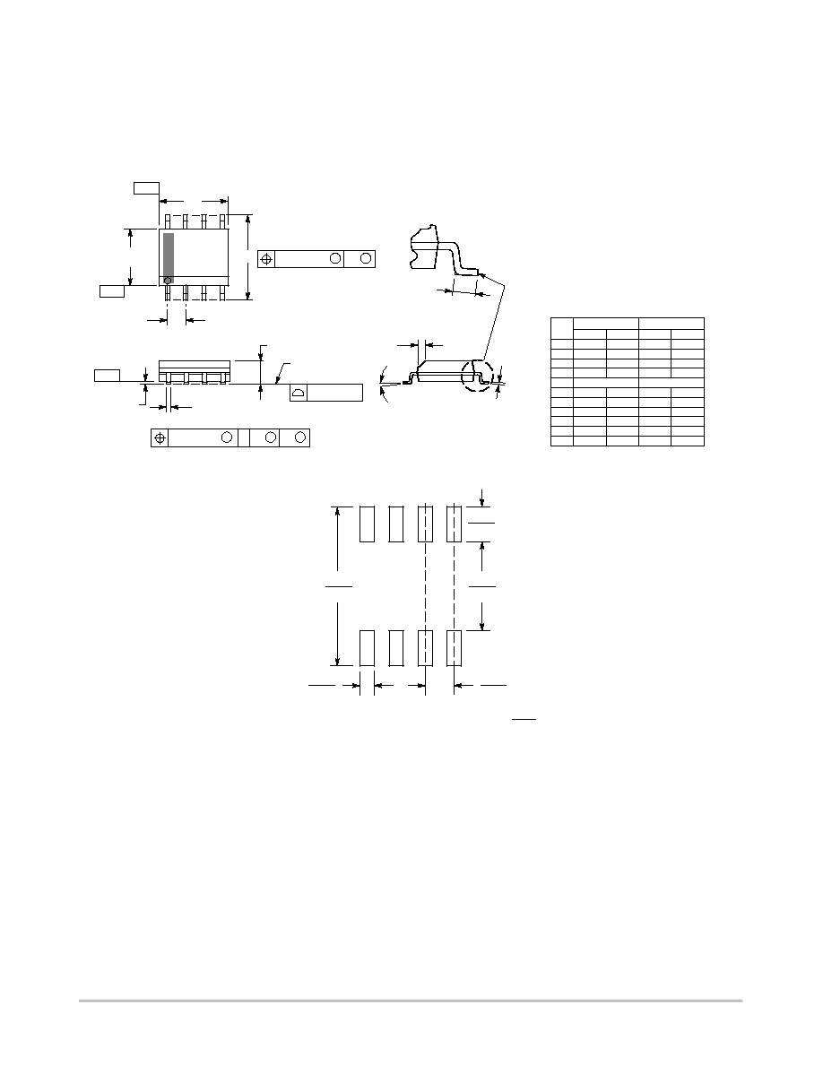
PACKAGE DIMENSIONS
SOIC-8
D SUFFIX
CASE 751-07
ISSUE AH
SEATING
PLANE
1
4
5
8
N
J
X 45
_
K
NOTES:
1. DIMENSIONING AND TOLERANCING PER
ANSI Y14.5M, 1982.
2. CONTROLLING DIMENSION: MILLIMETER.
3. DIMENSION A AND B DO NOT INCLUDE
MOLD PROTRUSION.
4. MAXIMUM MOLD PROTRUSION 0.15 (0.006)
PER SIDE.
5. DIMENSION D DOES NOT INCLUDE DAMBAR
PROTRUSION. ALLOWABLE DAMBAR
PROTRUSION SHALL BE 0.127 (0.005) TOTAL
IN EXCESS OF THE D DIMENSION AT
MAXIMUM MATERIAL CONDITION.
6. 751-01 THRU 751-06 ARE OBSOLETE. NEW
STANDARD IS 751-07.
A
B
S
D
H
C
0.10 (0.004)
DIM
A
MIN
MAX
MIN
MAX
INCHES
4.80
5.00
0.189
0.197
MILLIMETERS
B
3.80
4.00
0.150
0.157
C
1.35
1.75
0.053
0.069
D
0.33
0.51
0.013
0.020
G
1.27 BSC
0.050 BSC
H
0.10
0.25
0.004
0.010
J
0.19
0.25
0.007
0.010
K
0.40
1.27
0.016
0.050
M
0
8
0
8
N
0.25
0.50
0.010
0.020
S
5.80
6.20
0.228
0.244
-X-
-Y-
G
M
Y
M
0.25 (0.010)
-Z-
Y
M
0.25 (0.010)
Z
S
X
S
M
_
_
_
_
1.52
0.060
7.0
0.275
0.6
0.024
1.270
0.050
4.0
0.155
mm
inches
SCALE 6:1
*For additional information on our Pb-Free strategy and soldering
details, please download the ON Semiconductor Soldering and
Mounting Techniques Reference Manual, SOLDERRM/D.
SOLDERING FOOTPRINT*
NCP1582, NCP1582A, NCP1583
http://onsemi.com
16
ON Semiconductor and are registered trademarks of Semiconductor Components Industries, LLC (SCILLC). SCILLC reserves the right to make changes without further notice
to any products herein. SCILLC makes no warranty, representation or guarantee regarding the suitability of its products for any particular purpose, nor does SCILLC assume any liability
arising out of the application or use of any product or circuit, and specifically disclaims any and all liability, including without limitation special, consequential or incidental damages.
"Typical" parameters which may be provided in SCILLC data sheets and/or specifications can and do vary in different applications and actual performance may vary over time. All
operating parameters, including "Typicals" must be validated for each customer application by customer's technical experts. SCILLC does not convey any license under its patent rights
nor the rights of others. SCILLC products are not designed, intended, or authorized for use as components in systems intended for surgical implant into the body, or other applications
intended to support or sustain life, or for any other application in which the failure of the SCILLC product could create a situation where personal injury or death may occur. Should
Buyer purchase or use SCILLC products for any such unintended or unauthorized application, Buyer shall indemnify and hold SCILLC and its officers, employees, subsidiaries, affiliates,
and distributors harmless against all claims, costs, damages, and expenses, and reasonable attorney fees arising out of, directly or indirectly, any claim of personal injury or death
associated with such unintended or unauthorized use, even if such claim alleges that SCILLC was negligent regarding the design or manufacture of the part. SCILLC is an Equal
Opportunity/Affirmative Action Employer. This literature is subject to all applicable copyright laws and is not for resale in any manner.
PUBLICATION ORDERING INFORMATION
N. American Technical Support: 800-282-9855 Toll Free
USA/Canada
Japan: ON Semiconductor, Japan Customer Focus Center
2-9-1 Kamimeguro, Meguro-ku, Tokyo, Japan 153-0051
Phone: 81-3-5773-3850
NCP1582/D
LITERATURE FULFILLMENT:
Literature Distribution Center for ON Semiconductor
P.O. Box 61312, Phoenix, Arizona 85082-1312 USA
Phone: 480-829-7710 or 800-344-3860 Toll Free USA/Canada
Fax: 480-829-7709 or 800-344-3867 Toll Free USA/Canada
Email: orderlit@onsemi.com
ON Semiconductor Website: http://onsemi.com
Order Literature: http://www.onsemi.com/litorder
For additional information, please contact your
local Sales Representative.