©
Semiconductor Components Industries, LLC, 2006
April, 2006 - Rev. 1
1
Publication Order Number:
NCP1595/D
NCP1595, NCP1595A
Current Mode PWM
Converter for Low Voltage
Outputs
The NCP1595/NCP1595A is a current mode PWM buck converter
with integrated power switch and synchronous rectifier. It can provide
up to 1.5 A output current with high conversion efficiency. High
frequency PWM control scheme can provide a low output ripple noise.
Thus, it allows the usage of small size passive components to reduce
the board space. In a low load condition, the controller will
automatically change to PFM mode for provides a higher efficiency at
low load. Additionally, the device includes soft-start, thermal
shutdown with hysteresis, cycle-by-cycle current limit, and short
circuit protection. This device is available in compact 3x3 DFN
package.
Features
∑
High Efficiency 95% @ 3.375 V
∑
Synchronous Rectification for Higher Efficiency in PWM Mode
∑
Integrated MOSFET
∑
Fully Internal Compensation
∑
High Switching Frequency, 1.0 MHz
∑
Low Output Ripple
∑
Cycle-by-cycle Current Limit
∑
Current Mode Control
∑
Short Circuit Protection
∑
Built-in Slope Compensation for Current Mode PWM Converter
∑
$1.5% Reference Voltage
∑
Thermal Shutdown with Hysteresis
∑
Ext. Adjustable Output Voltage
∑
Fast Transient Response
∑
Low Profile and Minimum External Components
∑
Designed for Use with Ceramic Capacitor
∑
Compact 3x3 DFN Package
∑
These are Pb-Free Devices
Typical Applications
∑
Hard Disk Drives
∑
USB Power Device
∑
Wireless and DSL Modems
DFN6 3*3 MM, 0.95 PITCH
CASE 506AH
MARKING DIAGRAMS
http://onsemi.com
1
A
= Assembly Location
L
= Wafer Lot
Y
= Year
W
= Work Week
G
= Pb-Free Package
1595A
ALYW
G
1
N1595
ALYW
G
1
NC
VCC
VCCP
FB
GND
LX
EN
VCC
VCCP
FB
GND
LX
1595
1595A
PIN CONNECTIONS
See detailed ordering and shipping information in the package
dimensions section on page 11 of this data sheet.
ORDERING INFORMATION
NCP1595, NCP1595A
http://onsemi.com
2
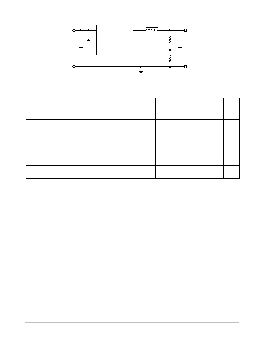
NCP1595
VCC
VCCP
EN
LX
FB
GND
R1
R2
C1
C2
L1
V
OUT
= 0.8 V to 0.9 x V
IN
V
IN
= 4.0 V to 5.5 V
Figure 1. Typical Operating Circuit
ABSOLUTE MAXIMUM RATINGS
Rating
Symbol
Value
Unit
Power Supply (Pin 4, 5)
V
IN
7.0
-0.3 (DC)
-1.0 (100 ns)
V
Input / Output Pins
Pin 1,3,6
V
IO
6.5,
-0.3 (DC)
-1.0 (100 ns)
V
Thermal Characteristics
3x3 DFN Plastic Package
Maximum Power Dissipation @ T
A
= 25
∞
C
Thermal Resistance Junction-to-Air
P
D
R
q
JA
1450
68.5
mW
∞
C/W
Operating Junction Temperature Range (Note 4)
T
J
-40 to + 150
∞
C
Operating Ambient Temperature Range
T
A
-40 to + 85
∞
C
Storage Temperature Range
T
stg
- 55 to +150
∞
C
Moisture Sensitivity Level (Note 3)
1
-
Stresses exceeding Maximum Ratings may damage the device. Maximum Ratings are stress ratings only. Functional operation above the
Recommended Operating Conditions is not implied. Extended exposure to stresses above the Recommended Operating Conditions may affect
device reliability.
NOTE:
ESD data available upon request.
1. This device series contains ESD protection and exceeds the following tests:
Human Body Model (HBM) 2.0 kV per JEDEC standard: JESD22-A114.
Machine Model (MM) 200 V per JEDEC standard: JESD22-A115.
2. Latchup Current Maximum Rating: 150 mA per JEDEC standard: JESD78.
3. Moisture Sensitivity Level (MSL): 1 per IPC/JEDEC standard: J-STD-020A.
4. The maximum package power dissipation limit must not be exceeded.
P
D
+
T
J(max)
*
T
A
R
q
JA
NCP1595, NCP1595A
http://onsemi.com
3
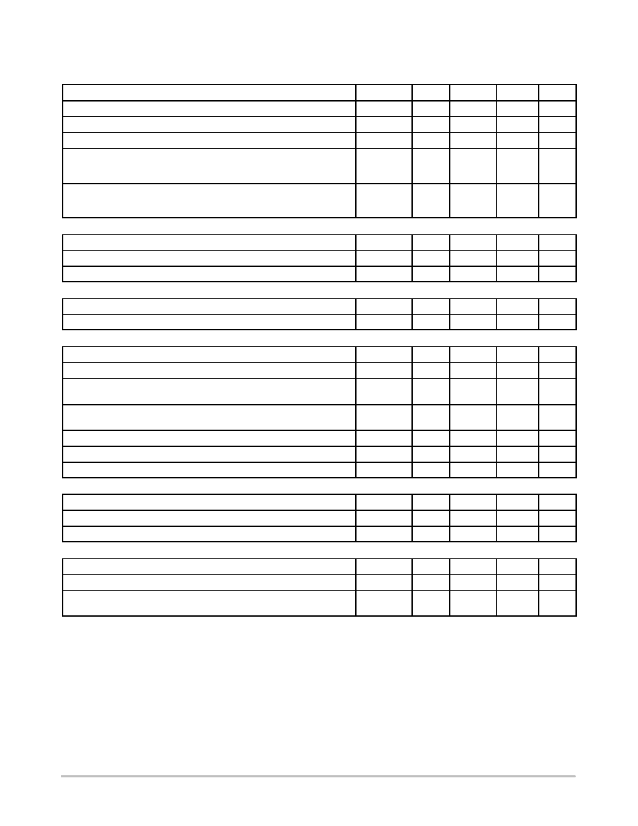
ELECTRICAL CHARACTERISTICS
(V
IN
= 5.0 V, V
OUT
= 1.2 V, T
A
= 25
∞
C for typical value, -40
∞
C
v
T
A
v
85
∞
C for min/max values unless otherwise noted)
Characteristic
Symbol
Min
Typ
Max
Unit
Operating Voltage
V
IN
4.0
-
5.5
V
Under Voltage Lockout Threshold
V
UVLO
3.2
3.5
3.8
V
Under Voltage Lockout hysteresis
V
UVLO_HYS
180
mV
P FET Leakage Current (Pin 5, 4)
T
A
= 25
∞
C
T
A
= -40
∞
C to 85
∞
C
I
LEAK-P
1.0
10
15
m
A
N FET Leakage Current (Pin 3, 2)
T
A
= 25
∞
C
T
A
= -40
∞
C to 85
∞
C
I
LEAK-N
1.0
10
15
m
A
FEEDBACK VOLTAGE
FB Input Threshold (T
A
= -40
∞
C to 85
∞
C)
V
FB
0.788
0.800
0.812
V
FB Input Current
I
FB
10
100
nA
Overvoltage Protect Higher than FB Threshold (T
A
= 25
∞
C)
V
OVP
2.0
5.0
10.0
%
THERMAL SHUTDOWN
Thermal Shutdown Threshold (Note 5)
T
SHDN
TBD
160
-
∞
C
Hysteresis
T
SDHYS
30
∞
C
PWM SMPS MODE
Minimum ON-Time
TON
MIN
100
ns
Switching Frequency (T
A
= -40
∞
C to 85
∞
C)
F
OSC
0.8
1.0
1.2
MHz
Internal PFET ON-Resistance (I
LX
= 100 mA, V
IN
= 5.0 V, T
A
= 25
∞
C)
(Note 5)
R
DS(ON)_P
-
0.2
0.3
W
Internal NFET ON-Resistance (I
LX
= 100 mA, V
IN
= 5.0 V, T
A
= 25
∞
C)
(Note 5)
R
DS(ON)_N
-
0.15
0.22
W
Maximum Duty Cycle
D
MAX
-
-
100
%
Soft-Start Time (V
IN
= 5.0 V, V
o
= 1.2 V, I
LOAD
= 0 mA, T
A
= 25
∞
C) (Note 6)
T
SS
-
1.0
-
ms
Main PFET Switch Current Limit (Note 5)
I
LIM
2.0
2.5
A
ENABLE (NCP1595A)
Enable Threshold High (NCP1595A Only)
V
EN_H
1.8
V
Enable Threshold Low
V
EN_L
0.4
V
Enable bias current ( EN = 0 V)
I
EN
500
TBD
nA
Total Device
Quiescent Current Into V
CCP
(V
IN
= 5 V, V
FB
= 1.0 V, T
A
= 25
∞
C)
I
CCP
10
m
A
Quiescent Current Into V
CC
(V
IN
= 5 V, V
FB
= 1.0 V, T
A
= 25
∞
C)
I
CC
900
m
A
Shutdown Quiescent Current into V
CC
and V
CCP
(NCP1595A Only)
(EN = 0, V
IN
= 5 V, V
FB
= 1.0 V, T
A
= 25
∞
C)
I
CC_SD
1.5
3.0
m
A
5. Values are design guarantee.
6. Design guarantee, value depends on voltage at V
OUT
.

NCP1595, NCP1595A
http://onsemi.com
4
PIN FUNCTION DESCRIPTIONS
Pin #
Symbol
Pin Description
NCP1595
1
FB
Feedback pin. Part is internally compensated. Only necessary to place a voltage divider or connect the out-
put directly to this pin.
2
GND
Ground
3
LX
Pin connected internally to power switch. Connect externally to inductor.
4
VCCP
Power connection to the power switch.
5
VCC
IC power connection.
6
NC
No Connection
NCP1595A
1
FB
Feedback pin. Part is internally compensated. Only necessary to place a voltage divider or connect the out-
put directly to this pin.
2
GND
Ground
3
LX
Pin connected internally to power switch. Connect externally to inductor.
4
VCCP
Power connection to the power switch.
5
VCC
IC power connection.
6
EN
Device Enable pin. This pin has an internal current source pull up. No connect is enable the device. With this
pin pulled down below 0.4 V, the device is disabled and enters the shutdown mode.
-
+
-
+
-
+
Power Reset
Under Voltage
Logout
Thermal
Shutdown
Control Logic
Oscillator
L1
C2
R1
R2
Soft Start
VCC
VCCP
NC/EN
FB
LX
GND
C1
Over Voltage
Protection
+
V
IN
Figure 2. Detail Block Diagram
V
OUT
= 0.8 V
to 0.9
V
IN

NCP1595, NCP1595A
http://onsemi.com
5
EXTERNAL COMPONENT REFERENCE DATA
Device
V
OUT
Inductor Model
Inductor (L1)
C
IN
(C1)
C
OUT
(C2)
R1
R2
NCP1595/
NCP1595A
3.3 V
CDC5D23 3R3 (1 A)
CDRH6D38 3R3 (1.5 A)
3.3
m
H
22
m
F
22
m
F x 2
22
m
F
22
m
F x 2
31 k
10 k
NCP1595/
NCP1595A
2.5 V
CDC5D23 3R3 (1 A)
CDRH6D38 3R3 (1.5 A)
3.3
m
H
22
m
F
22
m
F x 2
22
m
F
22
m
F x 2
21 k
10 k
NCP1595/
NCP1595A
1.5 V
CDC5D23 3R3 (1 A)
CDRH6D38 3R3 (1.5 A)
3.3
m
H
22
m
F
22
m
F x 2
22
m
F
22
m
F x 2
8 k
10 k
NCP1595/
NCP1595A
1.2 V
CDC5D23 3R3 (1 A)
CDRH6D38 3R3 (1.5 A)
3.3
m
H
22
m
F
22
m
F x 2
22
m
F
22
m
F x 2
5 k
10 k
NCP1595, NCP1595A
http://onsemi.com
6
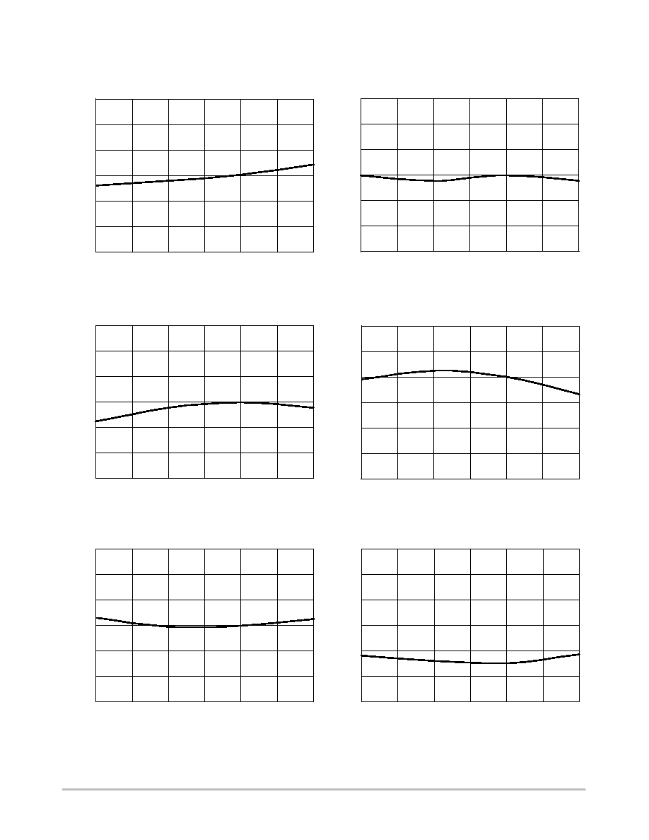
TYPICAL OPERATING CHARACTERISTICS
LOW SIDE AMBIENT TEMPERATURE, (T
A
/
∞
C)
0.00
0.05
0.10
0.15
0.20
0.25
0.30
-40
0
25
85
Figure 3. Switch ON Resistance vs.
Temperature
LOW SIDE SWITCH ON RESIST
ANCE/
W
Figure 4. Feedback Input Threshold vs.
Temperature
0.785
0.790
0.795
0.800
0.805
0.810
0.815
-40
0
25
85
AMBIENT TEMPERATURE, (T
A
/
∞
C)
F
B
INPUT THRESHOLD V
FB
/V
Figure 5. Switching Frequency vs.
Temperature
0.7
0.8
0.9
1.0
1.1
1.2
1.3
-40
0
25
85
AMBIENT TEMPERATURE, (T
A
/
∞
C)
SWITCH FREQUENCY
,
F
OSC
/MHZ
Figure 6. Main P-FET Current Limit vs.
Temperature
1.5
1.8
2.0
2.3
2.5
2.8
3.0
-40
0
25
85
AMBIENT TEMPERATURE, (T
A
/
∞
C)
MAIN P-FET CURRENT LIMIT
, I
LIM
/V
600
700
800
900
1000
1100
1200
-40
0
25
85
AMBIENT TEMPERATURE, (T
A
/
∞
C)
QUIESCENT CURRENT INT
O
V
CC
, I
CC
/
m
A
Figure 7. Quiescent Current Into V
CC
vs.
Temperature
0
1
2
3
4
5
6
-40
0
25
85
SHUTDOWN
QUIESCENT CURRENT
, I
CC_SD
/
m
A
AMBIENT TEMPERATURE, (T
A
/
∞
C)
Figure 8. Shutdown Quiescent Current vs.
Temperature
NCP1595, NCP1595A
http://onsemi.com
7
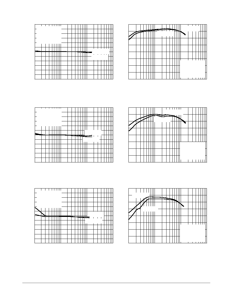
Figure 9. Output Voltage Change vs. Output
Current
Figure 10. Efficiency vs. Output Current
Figure 11. Output Voltage Change vs.
Output Current
Figure 12. Efficiency vs. Output Current
Figure 13. Efficiency vs. Output Current
Figure 14. Output Voltage Change vs.
Output Current
-1.5
-1.0
-0.5
0.0
0.5
1.0
1.5
10
100
1000
10000
V
OUT
= 3.3 V
L = 3.3
m
H
C
IN
= 22
m
F
C
OUT
= 22
m
F
V
IN
= 4.0 V
V
IN
= 5.0 V
20
30
40
50
60
70
80
90
100
10
100
1000
10000
V
OUT
= 3.3 V
L = 3.3
m
H
C
IN
= 22
m
F
C
OUT
= 22
m
F
V
IN
= 4.0 V
V
IN
= 5.0 V
-1.5
-1.0
-0.5
0.0
0.5
1.0
1.5
10
100
1000
10000
V
IN
= 4.0 V
V
IN
= 5.0 V
V
OUT
= 1.8 V
L = 3.3
m
H
C
IN
= 22
m
F
C
OUT
= 22
m
F
20
30
40
50
60
70
80
90
100
10
100
1000
10000
V
IN
= 4.0 V
V
IN
= 5.0 V
V
OUT
= 1.8 V
L = 3.3
m
H
C
IN
= 22
m
F
C
OUT
= 22
m
F
-1.5
-1.0
-0.5
0.0
0.5
1.0
1.5
10
100
1000
10000
V
IN
= 4.0 V
V
IN
= 5.0 V
V
OUT
= 1.2 V
L = 3.3
m
H
C
IN
= 22
m
F
C
OUT
= 22
m
F
20
30
40
50
60
70
80
90
100
10
100
1000
10000
V
IN
= 4.0 V
V
IN
= 5.0 V
V
OUT
= 1.2 V
L = 3.3
m
H
C
IN
= 22
m
F
C
OUT
= 22
m
F
OUTPUT
EFFICIENCY
, %
OUTPUT
EFFICIENCY
, %
OUTPUT
EFFICIENCY
, %
OUTPUT VOL
T
AGE CHANGE,
D
V
OUT
/%
OUTPUT VOL
T
AGE CHANGE,
D
V
OUT
/%
OUTPUT VOL
T
AGE CHANGE,
D
V
OUT
/%

NCP1595, NCP1595A
http://onsemi.com
8
(V
IN
= 5 V, I
LOAD
= 700 mA, L = 3.3
m
H, C
OUT
= 20
m
F)
Upper Trace: L
X
Pin Switching Waveform, 2 V / div.
Middle Trace: Output Ripple Voltage, 20 mV / div.
Lower Trace: Inductor Current, 1 A / div.
(V
IN
= 5 V, I
LOAD
= 100 mA, L = 3.3
m
H, C
OUT
= 20
m
F)
Upper Trace: L
X
Pin Switching Waveform, 2 V / div.
Middle Trace: Output Ripple Voltage, 20 mV / div.
Lower Trace: Inductor Current, 1 A / div.
Figure 15. DCM Switching Waveform for
V
OUT
= 3.3 V
Figure 16. CCM Switching Waveform for
V
OUT
= 3.3 V
(V
IN
= 5 V, I
LOAD
= 100 mA, L = 3.3
m
H, C
OUT
= 20
m
F)
Upper Trace: L
X
Pin Switching Waveform, 2 V / div.
Middle Trace: Output Ripple Voltage, 20 mV / div.
Lower Trace: Inductor Current, 1 A / div.
(V
IN
= 5 V, I
LOAD
= 700 mA, L = 3.3
m
H, C
OUT
= 20
m
F)
Upper Trace: L
X
Pin Switching Waveform, 2 V / div.
Middle Trace: Output Ripple Voltage, 20 mV / div.
Lower Trace: Inductor Current, 1 A / div.
Figure 17. DCM Switching Waveform for
V
OUT
= 1.2 V
Figure 18. CCM Switching Waveform for
V
OUT
= 1.2 V
(V
IN
= 5 V, I
LOAD
= 10 mA, L = 3.3
m
H, C
OUT
= 20
m
F x 2)
Upper Trace: Input Voltage, 2 V/ div.
Middle Trace: Output Voltage, 1 V/ div.
Lower Trace: Input Current, 1 A / div.
(V
IN
= 5 V, I
LOAD
= 10 mA, L = 3.3
m
H, C
OUT
= 20
m
F x 2)
Upper Trace: Input Voltage, 2 V/ div.
Middle Trace: Output Voltage, 1 V / div.
Lower Trace: Input Current, 1 A / div.
Figure 19. Soft-Start Waveforms for V
OUT
= 3.3 V
Figure 20. Soft-Start Waveforms for V
OUT
= 1.2 V

NCP1595, NCP1595A
http://onsemi.com
9
(V
IN
= 5 V, L = 3.3
m
H, C
OUT
= 20
m
F x 2)
Upper Trace: Output Dynamic Voltage, 100 mV / div.
Lower Trace: Output Current, 500 mA / div.
(V
IN
= 5 V, L = 3.3
m
H, C
OUT
= 20
m
F x 2)
Upper Trace: Output Dynamic Voltage, 100 mV / div.
Lower Trace: Output Current, 500 mA / div.
(V
IN
= 5 V, L = 3.3 H, C
OUT
= 20
m
F x 2)
Upper Trace: Output Dynamic Voltage, 100 mV / div.
Lower Trace: Output Current, 500 mA / div.
(V
IN
= 5 V, L = 3.3 H, C
OUT
= 20
m
F x 2)
Upper Trace: Output Dynamic Voltage, 100 mV / div.
Lower Trace: Output Current, 500 mA / div.
Figure 21. Load Regulation for V
OUT
= 3.3 V
Figure 22. Load Regulation for V
OUT
= 3.3 V
Figure 23. Load Regulation for V
OUT
= 1.2 V
Figure 24. Load Regulation for V
OUT
= 1.2 V

NCP1595, NCP1595A
http://onsemi.com
10
DETAILED OPERATING DESCRIPTION
Introduction
NCP1595 operates as a current mode buck converter with
switching frequency at 1.0 MHz. The P-Channel main
switch is set by the positive edge of the clock cycle going
into the PWM latch. The main switch is reset by the
PWM latch in the following three cases:
1. PWM comparator output trips as the peak inductor
current signal reaches a threshold level established
by the error amplifier.
2. The inductor current has reached the current limit.
3. Overvoltage at output occurs.
After a minimum dead time, the N-Channel synchronized
switch will turn on and the inductor current will ramp down.
If the inductor current ramps down to zero before the
initiation of next clock cycle, the regulator runs at
discontinuous conduction mode (DCM). Otherwise the
regulator is at continuous conduction mode (CCM). The
N-Channel switch will turn off when the clock cycle starts.
The duty cycle is given by the ratio of output voltage to input
voltage. The duty cycle is allowed to go to 100% to increase
transient load response when going from light load to heavy
load.
Error Amplifier and Slope Compensation
A fully internal compensated error amplifier is provided
inside NCP1595. No external circuitry is needed to stabilize
the device. The error amplifier provides an error signal to the
PWM comparator by comparing the feedback voltage
(800 mV) with internal voltage reference of 1.2 V.
Current mode converter can exhibit instability at duty
cycles over 50%. A slope compensation circuit is provided
inside NCP1595 to overcome the potential instability. Slope
compensation consists of a ramp signal generated by the
synchronization block and adding this to the inductor
current signal. The summed signal is then applied to the
PWM comparator.
Soft-Start and Current Limit
A soft start circuit is internally implemented to reduce the
in-rush current during startup. This helps to reduce the
output voltage overshoot.
The current limit is set to allow peak switch current in
excess of 2 A. The intended output current of the system is
1.5 A. The ripple current is calculated to be approximately
350 mA with a 3.3
mH inductor. Therefore, the peak current
at 1.5 A output will be approximately 1.7 A. A 2 A set point
will allow for transient currents during load step. The current
limit circuit is implemented as a cycle-by-cycle current
limit. Each on-cycle is treated as a separate situation.
Current limiting is implemented by monitoring the
P-Channel switch current buildup during conduction with a
current limit comparator. The output of the current limit
comparator resets the PWM latch, immediately terminating
the current cycle.
Over-Voltage Protection
Overvoltage occurs when the feedback voltage exceeds
5% of its regulated voltage. In this case, the P-Channel main
switch will be reset and the N-Channel synchronized switch
is turn on to sink current from the output voltage which helps
to drop its feedback voltage back to the regulated voltage.
Thermal Shutdown
Internal Thermal Shutdown circuitry is provided to
protect the integrated circuit in the event when maximum
junction temperature is exceeded. When activated, typically
at 160
∞C, the shutdown signal will disable the P-Channel
and N-Channel switch. The thermal shutdown circuit is
designed with 30
∞C of hysteresis. This means that the
switching will not start until the die temperature drops by
this amount. This feature is provided to prevent catastrophic
failures from accidental device overheating. It is not
intended as a substitute for proper heat sinking.
NCP1595 is contained in the thermally enhanced
DFN package.

NCP1595, NCP1595A
http://onsemi.com
11
APPLICATION INFORMATION
Output Voltage Selection
The output voltage is programmed through an external
resistor divider connect from V
OUT
to FB then to GND.
For internal compensation and noise immunity, the
resistor from FB to GND should be in 10 k to 20 k ranges.
The relationship between the output voltage and feedback
resistor is given by:
V
OUT
+
V
FB
1
)
R1
R2
(eq. 1)
V
OUT
: Output voltage
V
FB
: Feedback Voltage
R1: Feedback resistor from V
OUT
to FB.
R2: Feedback resistor from FB to GND.
Input Capacitor selection
In the PWM buck converter, the input current is pulsating
current with switching noise. Therefore, a bypass input
capacitor must choose for reduce the peak current drawn
from the power supply. For NCP1595, low ESR ceramic
capacitor of 10
mF should be used for most of cases. Also,
the input capacitor should be placed as close as possible to
the V
CCA
pin for effective bypass the supply noise.
Inductor selection
The inductor parameters are including three items, which
are DC resistance, inductor value and saturation current.
Inductor DC resistance will effect the convector overall
efficiency, low DC resistor value can provide a higher
efficiency. Thus, inductor value are depend on the inductor
ripple current, input voltage, output voltage, output current
and operation frequency, the inductor value is given by:
D
IL
+
V
OUT
L
F
SW
1
*
V
OUT
V
IN
(eq. 2)
DIL : peak to peak inductor ripple current
L: inductor value
FSW: switching frequency
After selected a suitable value of the inductor, it should be
check out the inductor saturation current. The saturation
current of the inductor should be higher than the maximum
load plus the ripple current.
D
IL(MAX)
+ D
IOUT(MAX)
)
D
IL
2
(eq. 3)
D
IL(MAX)
: Maximum inductor current
D
IOUT(MAX)
: Maximum output current
Output Capacitor selection
Output capacitor value is based on the target output ripple
voltage. For NCP1595, the output capacitor is required a
ceramic capacitors with low ESR value. Assume buck
converter duty cycle is 50%. The output ripple voltage in
PWM mode is given by:
D
VOUT
[ D
IL
1
4
FSW
C
OUT
)
ESR
(eq. 4)
In general, value of ceramic capacitor using 20
mF should
be a good choice.
ORDERING INFORMATION
Device
Package
Shipping
NCP1595MNR2G
DFN-6
(Pb-Free)
3000 / Tape & Reel
NCP1595AMNR2G
DFN-6
(Pb-Free)
3000 / Tape & Reel
For information on tape and reel specifications, including part orientation and tape sizes, please refer to our Tape and Reel Packaging
Specifications Brochure, BRD8011/D.

NCP1595, NCP1595A
http://onsemi.com
12
PACKAGE DIMENSIONS
DFN6 3*3 MM, 0.95 PITCH
CASE 506AH-01
ISSUE O
*For additional information on our Pb-Free strategy and soldering
details, please download the ON Semiconductor Soldering and
Mounting Techniques Reference Manual, SOLDERRM/D.
SOLDERING FOOTPRINT*
««««
««««
««««
PIN 1
REFERENCE
A
B
C
0.15
2X
2X
TOP VIEW
D
E
C
0.15
NOTES:
1. DIMENSIONS AND TOLERANCING PER ASME
Y14.5M, 1994.
2. CONTROLLING DIMENSION: MILLIMETERS.
3. DIMESNION b APPLIES TO PLATED TERMINAL
AND IS MEASURED BETWEEN 0.25 AND 0.30
MM FROM TERMINAL.
4. COPLANARITY APPLIES TO THE EXPOSED
PAD AS WELL AS THE TERMINALS.
3.31
0.130
0.63
0.025
2.60
0.1023
0.450
0.0177
1.700
0.685
mm
inches
SCALE 10:1
0.950
0.0374
E2
BOTTOM VIEW
b
0.10
6X
L
1
3
0.05
C A B
C
D2
4X
e
K
6
4
6X
6X
(A3)
C
C
0.08
6X
C
0.10
SIDE VIEW
A1
A
SEATING
PLANE
DIM
MIN
NOM
MAX
MILLIMETERS
A
0.80
0.90
1.00
A1
0.00
0.03
0.05
A3
0.20 REF
b
0.35
0.40
0.45
D
3.00 BSC
D2
2.40
2.50
2.60
E
3.00 BSC
E2
1.50
1.60
1.70
e
0.95 BSC
K
0.21
---
---
L
0.30
0.40
0.50
(NOTE 3)
ON Semiconductor and are registered trademarks of Semiconductor Components Industries, LLC (SCILLC). SCILLC reserves the right to make changes without further notice
to any products herein. SCILLC makes no warranty, representation or guarantee regarding the suitability of its products for any particular purpose, nor does SCILLC assume any liability
arising out of the application or use of any product or circuit, and specifically disclaims any and all liability, including without limitation special, consequential or incidental damages.
"Typical" parameters which may be provided in SCILLC data sheets and/or specifications can and do vary in different applications and actual performance may vary over time. All
operating parameters, including "Typicals" must be validated for each customer application by customer's technical experts. SCILLC does not convey any license under its patent rights
nor the rights of others. SCILLC products are not designed, intended, or authorized for use as components in systems intended for surgical implant into the body, or other applications
intended to support or sustain life, or for any other application in which the failure of the SCILLC product could create a situation where personal injury or death may occur. Should Buyer
purchase or use SCILLC products for any such unintended or unauthorized application, Buyer shall indemnify and hold SCILLC and its officers, employees, subsidiaries, affiliates,
and distributors harmless against all claims, costs, damages, and expenses, and reasonable attorney fees arising out of, directly or indirectly, any claim of personal injury or death
associated with such unintended or unauthorized use, even if such claim alleges that SCILLC was negligent regarding the design or manufacture of the part. SCILLC is an Equal
Opportunity/Affirmative Action Employer. This literature is subject to all applicable copyright laws and is not for resale in any manner.
PUBLICATION ORDERING INFORMATION
N. American Technical Support: 800-282-9855 Toll Free
USA/Canada
Japan: ON Semiconductor, Japan Customer Focus Center
2-9-1 Kamimeguro, Meguro-ku, Tokyo, Japan 153-0051
Phone: 81-3-5773-3850
NCP1595/D
LITERATURE FULFILLMENT:
Literature Distribution Center for ON Semiconductor
P.O. Box 61312, Phoenix, Arizona 85082-1312 USA
Phone: 480-829-7710 or 800-344-3860 Toll Free USA/Canada
Fax: 480-829-7709 or 800-344-3867 Toll Free USA/Canada
Email: orderlit@onsemi.com
ON Semiconductor Website: http://onsemi.com
Order Literature: http://www.onsemi.com/litorder
For additional information, please contact your
local Sales Representative.