
©
Semiconductor Components Industries, LLC, 2006
April, 2006 - Rev. 8
1
Publication Order Number:
NCP1603/D
NCP1603
PFC/PWM Combo Controller
with Integrated High
Voltage Startup and Standby
Capability
The NCP1603 is a Power Factor Correction (PFC) and Pulse Width
Modulation (PWM) combo controller. It offers extremely low
no-load standby power consumption that is suitable for the
low-power consumer markets. The key features of the device are
listed below.
Features
∑
Pb-Free Package is Available
*
PFC Features
∑
Near-Unity Power Factor in Discontinuous and Critical Mode
(DCM and CRM)
∑
Voltage-Mode Operation
∑
Low Startup and Shutdown Current Consumption
∑
Programmable Switching Frequency for DCM
∑
Synchronization Capability
∑
Overvoltage Protection (107% of Nominal Output Level)
∑
Undervoltage Protection or Shutdown
(8% of Nominal Output Level)
∑
Programmable Overcurrent Protection
∑
Thermal Shutdown with Hysteresis (95/140
∞C)
∑
Undervoltage Lockout with Hysteresis (9.0/10.5 V)
PWM Features
∑
Integrated Lossless High Voltage Startup Current Source
∑
100 kHz PWM Current-Mode Operation with Skipping Cycle
Capability During Standby Condition
∑
PFC Bias Voltage is Disabled in Standby Condition to Achieve
Extremely Low No-Load Standby Power Consumption
∑
Fault Protection Implemented by a Timer and Independent of Badly
Coupled Auxiliary Transformer Winding
∑
Primary Overcurrent Protection and Latched Overvoltage Protection
∑
Internal 2.5 ms Soft-Start
∑
"
6.4% Frequency Jittering for Improved EMI Performance
∑
Latched Thermal Shutdown with Hysteresis (140/165
∞C)
∑
Undervoltage Lockout with Hysteresis (5.6/7.7/12.6 V)
Applications
∑
Notebook Adapters
∑
TV/Monitors
*For additional information on our Pb-Free strategy and soldering details, please
download the ON Semiconductor Soldering and Mounting Techniques Reference
Manual, SOLDERRM/D.
http://onsemi.com
SO-16
D SUFFIX
CASE 751B
Device
Package
Shipping
ORDERING INFORMATION
NCP1603D100R2
SO-16
2500 Tape & Reel
MARKING
DIAGRAM
A
= Assembly Location
WL = Wafer Lot
Y
= Year
WW = Work Week
G
= Pb-Free Package
1
1603D100G
AWLYWW
1
2
3
4
5
6
7
8
16
15
14
12
11
10
9
(Top View
)
Osc
V
aux
FB2
CS2
GND2
GND1
Out1
V
CC1
HV
NC
Ramp
CS1
FB1
V
CC2
V
control
13 Out2
PIN CONNECTIONS
For information on tape and reel specifications,
including part orientation and tape sizes, please
refer to our Tape and Reel Packaging Specification
Brochure, BRD8011/D.
1
NCP1603D100R2G
SO-16
(Pb-Free)
2500 Tape & Reel
16

NCP1603
http://onsemi.com
2
AC
Input
EMI
Filter
NCP1603
OVP
Output
Voltage
+
-
Figure 1. Typical Application Circuits
AC
Input
EMI
Filter
NCP1603
OVP
Output
Voltage
+
-
Not Synchronized and V
CC
OVP Latch Implemented
Synchronized and Output OVP Latch Implemented

NCP1603
http://onsemi.com
3
I
S
UVLO
Current
Mirror
FB1
CS1
Regulation Block
Current
Mirror
Out1
GND1
Ramp
PFC
Osc
Thermal
Shutdown
PWM
-
LEB
125 ms
2.5 ms
Softstart
CS2
FB2
Oscillator
100 kHz
125 ms
delay
HV
S Q
R
3V
OVP
Out2
Gnd2
PWM
Standby
OR
5V
1V max
18k
55k
20k
25k
Fault-2
0.75V
0.75V/ 1.25V
Fault-2
OR
300k
OR
5ms Jittering
Zero Current
Protection
Overcurrent
Protection
Overvoltage
Shutdown / UVP
delay
Max duty
R Q
S
= 80%
200ns
(9 / 10.5V)
Voltage
Regulator
Internal bias
FB1
ref
ref
reg
V
I
I
96%I
(12.6 / 7.7V)
(5.6 / 4V)
1 0
0~2.3V ramp
100 kHz
5ms Jittering
R
S Q
&
&
S R
Q
1 0
S
R Q
&
start_Vaux
start_Vaux
3.9V max
clamp
&
+
-
+
-
+
-
+
-
+
-
+
11
9
5
16
8
2
3
4
1
6
7
12
10
14
13
10V
10V
9V
9V
18V
20V
9V
9V
Thermal
Shutdown
-
+
5/ 3.5 V
R
Q
S
0 1
delay
9 V
Detection
&
3.2mA
0 1
+
-
clock
disable
initially
Error
Fault-1
Vaux
Internal bias
PFC
Modulation
&
V
CC1
94
m
A
45
m
A
(I
FB1
< 8% I
REF
)
I
FB1
(I
FB1
> 107% I
REF
)
V
CS2
V
FB2
V
SS
(140/165
∞
C)
latchoff, reset
when V
CC2
< 4V
disable V
aux
when V
CC2
< 7.7V
V
CC2
mgmt
V
CC2
V
aux
V
control
I
ch
C
3
C
1
R
1
R
2
R
3
V
ton
V
CC1
(I
S
> 203
m
A)
(95/140
∞
C)
(I
S
< 14
m
A)
V
CC2
Figure 2. Functional Block Diagram
latchoff, reset
when V
CC2
< 4V
Fault-1

NCP1603
http://onsemi.com
4
PIN FUNCTION DESCRIPTION
Pin
Symbol
Function
Description
1
V
aux
Auxiliary Supply
This pin connects to the V
CC1
pin externally. It delivers a bias voltage from the V
CC2
to the
PFC section. The V
aux
is disabled when either one of the following conditions occurs:
(1) V
aux
is initially off;
(2) Fault (V
FB2
> 3.0 V for more than 125 ms);
(3) Standby (V
FB2
< 0.75 V and then V
FB2
is smaller than 1.25 V for more than 125 ms);
(4) Overvoltage protection latch activated from CS2 pin;
(5) Thermal shutdown latch in the PWM section;
(6) Insufficient supply voltage (V
CC2
< 7.7 V).
The transistor turns on (or V
aux
is enabled) when V
FB2
is within the normal mode regulation
window (0.75 V < V
FB2
< 3.0 V).
2
FB2
PWM Feedback
An external optocoupler collector pulls the voltage of this pin V
FB2
down to regulate the
output voltage. The PWM regulation window between V
FB2
= 0.75 V and V
FB2
= 3.0 V. When
V
FB2
drops below 0.75 V, the controller enters standby operation.
When no feedback signal is received from the optocoupler, V
FB2
is internally pulled to be
higher than 3.0 V. If this condition lasts for longer than 125 ms, the controller enters
double-hiccup fault condition.
3
CS2
PWM Current Sense
This pin cumulates three different functions: current-mode PWM regulation, primary
overcurrent protection and overvoltage protection (OVP). If the voltage of this pin is above
3.0 V for OVP, the circuit is latched off until V
CC2
resets. The PWM Drive Output is disabled.
An external noise decoupling pF-order capacitor is connected to the pin to prevent the latch
protection activated due to noise.
4
GND2
PWM Ground
-
5
Osc
PFC Oscillator
In oscillator mode, this pin is connected to an external capacitor to set the oscillator
frequency in DCM operation. In synchronization mode, this pin is connected to an external
driving signal. However, if the PFC-stage inductor current is non-zero at the end of a
switching period, the PFC-stage circuit will be forced to CRM and the Out1 is out of
synchronization to the Osc pin signal.
6
GND1
PFC Ground
-
7
Out1
PFC Drive Output
This pin provides an output to an external MOSFET in the PFC section.
8
V
CC1
PFC Supply Voltage
This pin is the positive supply of the PFC section. the operating range is between 9.0 V and
18 V with UVLO start threshold 10.5 V.
9
FB1
PFC Feedback
This pin receives a current I
FB1
that represents the PFC circuit output voltage. The current is
for the output regulation, PFC section overvoltage protection (OVP) and PFC section output
undervoltage protection (UVP). When I
FB1
goes above 107% I
ref
, OVP is activated and the
Drive Output is disabled. When I
FB1
goes below 14
m
A, the PFC section enters a
low-current consumption shutdown mode.
10
V
control
PFC Control Voltage
The control voltage V
control
directly controls the input impedance and hence the power factor
of the circuit. This pin is connected to an external capacitor to limit the control voltage
bandwidth typically below 20 Hz to achieve Power Factor Correction purpose.
11
CS1
PFC Current Sense
This pin receives a current I
S
that is proportional to the inductor current. The current is for
overcurrent protection (OCP), and zero current detection. When I
S
goes above 200
m
A, OCP
is activated and the Drive Output (Out1) is disabled. When I
S
goes below 14
m
A, it is
recognized to be a zero current for feedback regulation and DCM or CRM operation in the
PFC oscillator section.
12
Ramp
PFC Ramp
This pin is connected to an external capacitor to set a ramp signal. The capacitor value
directly affects the input impedance of the PFC circuit and its maximum input power.
13
Out2
PWM Drive Output
This pin provides an output to an external MOSFET in the PWM section.
14
V
CC2
PWM Supply Voltage
This pin is basically the positive supply of the PWM section. It is also the positive supply of
the whole device because the PFC section is also supplied from this pin indirectly through
V
aux
pin (Pin 1). The operating range is between 7.7 V and 18 V. The circuit resets when
V
CC2
drops below 4.0 V.
15
NC
No Connected
This pin is for high voltage clearance of the HV pin.
16
HV
High Voltage
This pin connects to the bulk DC voltage to deliver power to the controller in startup or fault
condition. The internal startup circuit is disabled in normal and standby condition for power
saving purpose. The UVLO stop and start thresholds of the startup circuit are V
CC2
= 12.6 V
and V
CC2
= 5.6 V.

NCP1603
http://onsemi.com
5
MAXIMUM RATINGS
Rating
Symbol
Value
Unit
V
aux
Pin (Pin 1)
Maximum Voltage Range
Maximum Continuous Current
V
max
I
max
-0.3 to +18
35
V
mA
FB2 and CS2 Pin (Pins 2-3)
Maximum Voltage Range
Maximum Current
V
max
I
max
-0.3 to +10
100
V
mA
Ramp, CS1, V
control
, FB1, and Osc Pins (Pins 5, 9-12)
Maximum Voltage Range
Maximum Current
V
max
I
max
-0.3 to +9.0
100
V
mA
Out1 Pin (Pin 7)
Maximum Voltage Range
Maximum Current
V
max
I
max
-0.3 to +18
-500 to +750
V
mA
V
CC1
and V
CC2
Pins (Pins 8, 14)
Maximum Voltage Range
Maximum Current
V
max
I
max
-0.3 to +18
100
V
mA
Out2 Pin (Pin 13)
Maximum Voltage Range
Maximum Current
V
max
I
max
-0.3 to +17.5
1.0
V
A
HV Pin (Pin 16)
Maximum Voltage Range
Maximum Current
V
max
I
max
-0.3 to +500
100
V
mA
Power Dissipation and Thermal Characteristics
Maximum Power Dissipation (T
A
= 25
∞
C)
Thermal Resistance, Junction-to-Air
P
D
R
q
JA
770
111
mW
∞
C/W
Operating Junction Temperature Range
T
J
-40 to +125
∞
C
Maximum Storage Temperature Range
T
stg
-60 to +150
∞
C
Stresses exceeding Maximum Ratings may damage the device. Maximum Ratings are stress ratings only. Functional operation above the
Recommended Operating Conditions is not implied. Extended exposure to stresses above the Recommended Operating Conditions may affect
device reliability.
1. This device contains ESD protection and exceeds the following tests:
Pin 1-14: Human Body Model 2000 V per Mil-Std-883, Method 3015.
Machine Model Method 200 V.
Pin 16 is the HV startup of the device and is rated to the maximum rating of the part, or 500 V.
2. This device contains latchup protection and exceeds 100 mA per JEDEC Standard JESD78.
NCP1603
http://onsemi.com
6
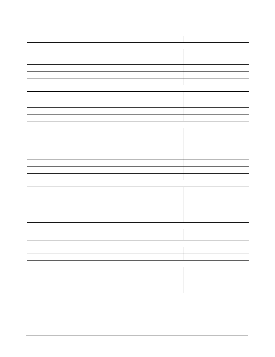
ELECTRICAL CHARACTERISTICS
(For typical values T
J
= 25
∞
C, for min/max values, T
J
= -40
∞
C to +125
∞
C, V
CC2
= 13 V,
HV = 30 V, V
CC1
= 15 V, V
control
= 100 nF, Ramp = 330 pF, Osc = 220 pF unless otherwise specified).
Characteristic (PWM Section)
Pin
Symbol
Min
Typ
Max
Unit
PWM OSCILLATOR
Oscillation Frequency (T
J
= 25
_
C) (Note 3)
Oscillation Frequency (T
J
= 0
_
C to +125
_
C)
Oscillation Frequency (T
J
= -40
_
C to +125
_
C)
-
f
osc2
93
90
85
100
-
-
107
110
110
kHz
Oscillator Modulation Swing, in Percentage of f
osc2
-
-
-
"
6.4
-
%
Oscillator Modulation Swing Period
-
-
-
5.0
-
ms
Maximum Duty Ratio (V
CS2
= 0 V, V
FB2
= 2.0 V)
-
D
max
75
80
85
%
PWM GATE DRIVE
Gate Drive Resistor
Output High (V
CC2
= 13 V, Out2 = 300
W
to GND2)
Output Low (Out2 = 1.0 V, V
FB2
= 0 V)
13
R
OH2
R
OL2
6.0
3.0
12.3
7.5
25
18
W
W
Gate Drive Rise Time from 10% to 90% (Out2 = 1.0 nF to GND2)
13
t
r2
-
40
-
ns
Gate Drive Fall Time from 90% to 10% (Out2 = 1.0 nF to GND2)
13
t
f2
-
15
-
ns
PWM CURRENT SENSE/OVERVOLTAGE PROTECTION
Maximum Current Threshold (T
J
= 25
_
C)
Maximum Current Threshold (T
J
= -40
_
C to +125
_
C)
3
I
Limit
0.991
0.96
1.043
-
1.095
1.106
V
Soft-Start Duration
-
t
SS
-
2.5
-
ms
Leading Edge Blacking Duration
3
t
LEB
100
200
350
ns
Propagation Delay from CS Detected to Turn Out2 Off
-
T
delay(CS)
-
90
180
ns
Overvoltage Protection Threshold
3
V
OVP
2.7
3.0
3.3
V
Internal Compensation Ramp (Peak-to-Peak) (Note 4)
3
V
comp
-
2.3
-
V
Internal Resistor to Ramp (Note 4)
3
R
comp
9.0
18
36
k
W
PWM STANDBY THRESHOLDS/FEEDBACK
Standby Thresholds
Feedback Voltage V
FB2
to Start Standby
Feedback Voltage V
FB2
to Stop Standby
2
V
stby
V
stby-out
0.6
1.0
0.75
1.25
0.9
1.5
V
V
Validation Time for Leaving Standby
2
t
stby-aux
-
125
-
ms
Validation Time for Recognize a Fault
2
t
fault
-
125
-
ms
Feedback Pin Sinking Capability (V
FB2
= 0.75 V)
2
I
FB2
200
235
270
m
A
AUXILIARY SUPPLY
V
aux
MOSFET Resistance
(V
CC2
= 13 V, V
FB
= 2.0 V, V
aux
= 20 mA Sinking)
1
R
aux
6.0
11.7
23
W
PWM THERMAL SHUTDOWN
Thermal Shutdown Threshold (Note 4)
-
T
SD2
150
165
-
∞
C
Thermal Shutdown Hysteresis
-
T
H2
-
25
-
∞
C
PWM STARTUP CURRENT SOURCE
High-Voltage Current Source
Startup (V
CC2
= V
CC2(on)
-0.2 V, V
FB2
= 2.0 V, HV = 30 V)
Startup (V
CC2
= 0 V, HV = 30 V)
Leakage (V
CC2
= 13 V, HV = 700 V)
16
I
HV1
I
HV2
I
HV3
1.8
1.8
10
3.2
4.4
30
4.2
5.6
80
mA
mA
m
A
Minimum Startup Voltage (V
CC2
= V
CC2(on)
-0.2 V, I
HV
= 0.5 mA)
16
V
start(min)
-
20
23
V
3. Consult factory for other frequency options.
4. Guaranteed by design.

NCP1603
http://onsemi.com
7
ELECTRICAL CHARACTERISTICS
(For typical values T
J
= 25
∞
C, for min/max values, T
J
= -40
∞
C to +125
∞
C, V
CC2
= 13 V,
HV = 30 V, V
CC1
= 15 V, V
control
= 100 nF, Ramp = 330 pF, Osc = 220 pF unless otherwise specified).
Characteristic (PFC Section)
Pin
Symbol
Min
Typ
Max
Unit
PWM SUPPLY SECTION
Supply Voltage
Startup Threshold, V
CC2
Increasing
Minimum Operating Valley Voltage after Turn-On
Undervoltage Lockout Threshold Voltage, V
CC2
Decreasing
Logic Reset Level
14
V
CC2(on)
V
CC2(off)
V
CC2(latch)
V
CC2(reset)
11.6
7.0
5.0
-
12.6
7.7
5.6
4.0
13.6
8.4
6.2
-
V
V
V
V
Supply Current
Operating (V
CC2
= 13 V, Out2 = Open, V
FB2
= 2.0 V)
Operating (V
CC2
= 13 V, Out2 = 1.0 nF to GND2, V
FB2
= 2.0 V)
Latch-Off Phase (V
CC2
= 6.5 V, V
FB2
= 2.0 V)
14
I
CC2(op1)
I
CC2(op2)
I
CC2(latch)
0.6
1.3
400
1.1
2.2
680
1.8
3.0
1000
mA
mA
m
A
PFC OSCILLATOR
Oscillator Frequency (Osc = 220 pF to GND)
5
f
osc1
52
58
64
kHz
Internal Capacitance of the Oscillator Pin
5
C
osc(int)
-
36
-
pF
Maximum Oscillator Switching Frequency
5
f
osc1(max)
-
405
-
kHz
Oscillator Discharge Current (Osc = 5.5 V)
5
I
odch
40
49
60
m
A
Oscillator Charge Current (Osc = 3.0 V)
5
I
och
40
45
60
m
A
Comparator Lower Threshold (Osc = 220 pF to GND) (Note 5)
5
V
sync(L)
3.0
3.5
4.0
V
Comparator Upper Threshold (Osc = 220 pF to GND)
5
V
sync(H)
4.5
5.0
5.5
V
Synchronization Pulse Width for Detection
5
t
sync(min)
500
-
-
ns
Synchronization Propagation Delay
5
t
sync(d)
-
371
-
ns
PFC GATE DRIVE
Gate Drive Resistor
Output High and Draw 100 mA out of Out1 Pin
(I
source
= 100 mA)
Output Low and Insert 100 mA into Out1 Pin
(I
sink
= 100 mA)
7
R
OH1
R
OL1
5.0
2.0
11.6
7.2
20
18
W
W
Gate Drive Rise Time from 1.5 V to 13.5 V
(Out1 = 1.0 nF to GND)
7
t
r1
-
53
-
ns
Gate Drive Fall Time from 13.5 V to 1.5 V
(Out1 = 1.0 nF to GND)
7
t
f1
-
32
-
ns
PFC FEEDBACK/OVERVOLTAGE PROTECTION/UNDERVOLTAGE PROTECTION
Reference Current
9
I
ref
192
203
208
m
A
Regulation Block Ratio
9
I
regL
/I
ref
95
96
97
%
Vcontrol Pin Internal Resistor
10
R
control
-
300
-
k
W
Maximum Control Voltage (I
FB1
= 100
m
A)
10
V
control(max)
0.95
1.05
1.15
V
Feedback Pin Voltage (I
FB1
= 100
m
A)
9
V
FB1-100
-
3.0
-
V
Overvoltage Protection Current Ratio
9
I
OVP
/I
ref
104
107
-
%
Overvoltage Protection Current Threshold
9
I
OVP
-
217
225
m
A
Undervoltage Protection Current Threshold
9
I
UVP
/I
ref
4.0
8.0
15
%
5. Comparator lower threshold is also the synchronization threshold.

NCP1603
http://onsemi.com
8
ELECTRICAL CHARACTERISTICS
(continued) (For typical values T
J
= 25
∞
C, for min/max values, T
J
= -40
∞
C to +125
∞
C,
V
CC2
= 13 V, HV = 30 V, V
CC1
= 15 V, V
control
= 100 nF, Ramp = 330 pF, Osc = 220 pF unless otherwise specified).
Characteristic (PFC Section)
Pin
Symbol
Min
Typ
Max
Unit
PFC CURRENT SENSE
Current Sense Pin Offset Voltage (I
S
= 100
m
A)
11
V
S
-
4.0
-
mV
Overcurrent Protection Level
11
I
S(OCP)
190
203
210
m
A
Current Sense Pin Offset Voltage at Overcurrent Level
11
V
S(OCP)
0
3.2
20
mV
Zero Current Detection Level
11
I
S(ZCD)
9
14
19
m
A
Current Sense Pin Offset Voltage at Zero Current Level
11
V
S(ZCD)
0
7.5
20
mV
Zero Current Sense Resistor (R
S(ZCD)
= V
S(ZCD)
/I
S(ZCD)
)
11
R
S(ZCD)
-
0.536
1.0
k
W
PFC RAMP
Charging Current (Ramp = 0 V)
12
I
ch
95
100
105
m
A
Maximum Power Resistance (R
power
= V
control(max)
/I
ch
)
12
R
power
9.5
10
11.5
k
W
Internal Clamping of Voltage V
ton
-
V
ton(max)
-
3.9
-
V
Internal Capacitance of the Ramp Pin
12
C
ramp(int)
-
22
-
pF
Ramp Pin Sink Resistance
(Osc = 0 V, Ramp = 1.0 mA sourcing)
12
R
ramp
-
71.5
-
W
PFC THERMAL SHUTDOWN
Thermal Shutdown Threshold (Note 6)
-
T
SD1
140
170
-
∞
C
Thermal Shutdown Hysteresis
-
T
H1
-
45
-
∞
C
PFC SUPPLY SECTION
Supply Voltage
Startup Threshold (UVLO)
Minimum Voltage for Operation after Turn-On
UVLO Hysteresis
8
V
CC1(on)
V
CC1(off)
V
H1
9.6
8.25
1.0
10.5
9.0
1.5
11.4
9.75
-
V
V
V
Supply Current
Start-Up (V
CC1
= V
CC1(on)
≠0.2 V)
Operating (V
CC1
= 15 V, Out1 = Open, Osc = 220 pF)
Operating (V
CC1
= 15 V, Out1 = 1.0 nF to GND1, Osc = 220 pF)
Shutdown (V
CC1
= 15 V, I
FB
= 0 A)
8
I
CC1(stup)
I
CC1(op1)
I
CC1(op2)
I
CC1(stdn)
-
-
-
-
17
2.7
3.7
24
40
5.0
5.0
50
m
A
mA
mA
m
A
6. Guaranteed by design.

NCP1603
http://onsemi.com
9
110
108
106
104
102
100
98
96
94
92
90
-50
-25
0
25
50
75
100
125
PWM SECTION OSCILLA
T
OR FREQUENCY (kHz
)
T
J
, JUNCTION TEMPERATURE (
∞
C)
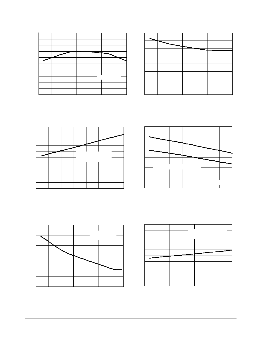
Figure 3. PWM Section Oscillator Frequency
vs. Temperature
10
8
6
4
2
0
-50
-25
0
25
50
75
100
125
PWM SECTION FREQUENCY JITTERING (%)
T
J
, JUNCTION TEMPERATURE (
∞
C)
Figure 4. PWM Section Oscillator Frequency
Jittering vs. Temperature
85
84
83
82
81
80
79
78
77
76
75
-50
-25
0
25
50
75
100
125
T
J
, JUNCTION TEMPERATURE (
∞
C)
Figure 5. PWM Section Maximum Duty
vs. Temperature
CS2 Pin = 0 V
FB2 Pin = 2 V
PWM SECTION MAXIMUM DUTY (%)
18
16
14
12
10
8
6
4
2
0
-50
-25
0
25
50
75
100
125
PWM SECTION GA
TE DRIVE RESIST
ANCE (
W
)
R
OH2
R
OL2
T
J
, JUNCTION TEMPERATURE (
∞
C)
Figure 6. PWM Section Gate Drive Resistance
vs. Temperature
1.1
1.05
1
0.95
0.9
-50
-25
0
25
50
75
100
125
PWM SECTION CURRENT LIMIT (V)
T
J
, JUNCTION TEMPERATURE (
∞
C)
Figure 7. PWM Section Current Limit
vs. Temperature
PWM SECTION SOFT-ST
A
R
T PERIOD (ms)
3
2.5
2
1.5
1
0.5
0
T
J
, JUNCTION TEMPERATURE (
∞
C)
-50
-25
0
25
50
75
100
125
Figure 8. PWM Section Soft-Start Period
vs. Temperature
12

NCP1603
http://onsemi.com
10
140
120
100
80
60
40
20
0
-50
-25
0
25
50
75
100
125
PWM SECTION V
ALIDA
TION TIME
FOR LEA
VING ST
ANDBY (ms)
T
J
, JUNCTION TEMPERATURE (
∞
C)
350
300
250
200
150
100
50
0
-50
-25
0
25
50
75
100
125
PWM SECTION LEAD EDGE BLANKING (ns)
T
J
, JUNCTION TEMPERATURE (
∞
C)
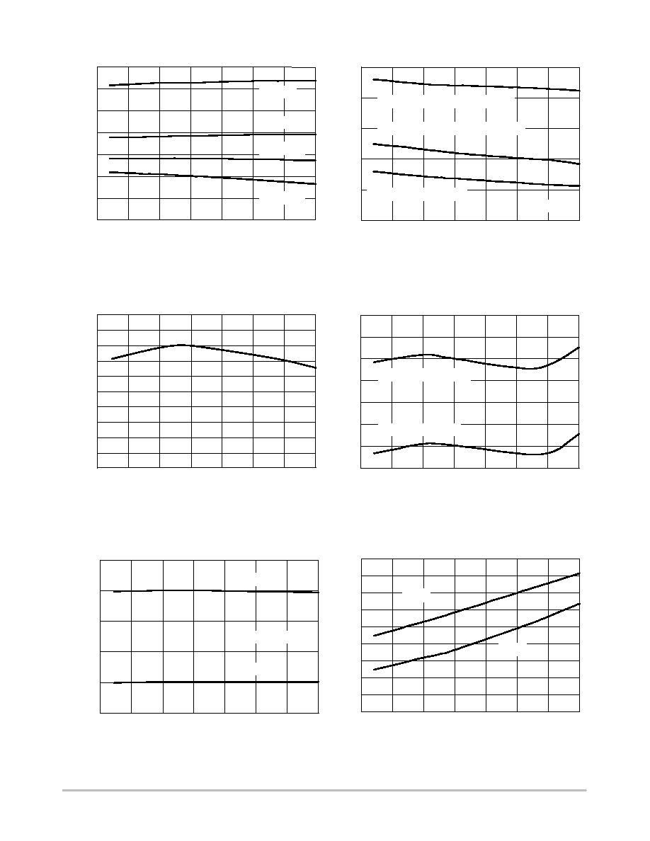
Figure 9. PWM Section Lead Edge Blanking
vs. Temperature
120
100
80
60
40
20
0
-50
-25
0
25
50
75
100
125
PWM SECTION CS PROP
A
G
A
TION DELA
Y (ns
)
T
J
, JUNCTION TEMPERATURE (
∞
C)
Figure 10. CS2 Pin Propagation Delay
vs. Temperature
-50
-25
0
25
50
75
100
125
T
J
, JUNCTION TEMPERATURE (
∞
C)
V
CS2
= 2 V
V
FB2
= 2 V
PWM SECTION MINIMUM PULSE (ns)
500
450
400
350
300
250
200
150
100
50
0
Figure 11. PWM Section Minimum Output Pulse
vs. Temperature
3.15
3.1
3.05
3
2.95
2.9
-50
-25
0
25
50
75
100
125
T
J
, JUNCTION TEMPERATURE (
∞
C)
Figure 12. CS2 Pin Overvoltage Protection
Threshold vs. Temperature
PWM SECTION CS PIN OVP THRESHOLD (V)
1.4
1.2
1
0.8
0.6
0.4
0.2
0
-50
-25
0
25
50
75
100
125
PWM SECTION ST
ANDBY THRESHOLDS (V)
T
J
, JUNCTION TEMPERATURE (
∞
C)
Figure 13. PWM Section Standby Thresholds
vs. Temperature
Figure 14. PWM Section Validation Time for
Leaving Standby vs. Temperature
V
stby-out
V
stby
160
NCP1603
http://onsemi.com
11
-50
-25
0
25
50
75
100
125
T
J
, JUNCTION TEMPERATURE (
∞
C)
V
FB2
= 0.75 V
PWM SECTION FB PIN SINKING CAP
ABILITY (
m
A
)
250
245
240
235
230
225
220
215
210
205
200
Figure 15. FB2 Pin Sinking Capability
vs. Temperature
140
120
100
80
60
40
20
0
-50
-25
0
25
50
75
100
125
PWM SECTION
V
ALIDA
TION
TIME FOR
RECOGNIZE A F
A
U
L
T (ms)
T
J
, JUNCTION TEMPERATURE (
∞
C)
Figure 16. PWM Section Validation Time for
Recognizing a Fault vs. Temperature
-50
-25
0
25
50
75
100
125
T
J
, JUNCTION TEMPERATURE (
∞
C)
V
aux
= 20 mA Sinking
V
CC2
= 13 V
V
aux
PIN MOSFET RESIST
ANCE (
W
)
20
18
16
14
12
10
8
6
4
2
0
Figure 17. V
aux
Pin Internal MOSFET
Resistance vs. Temperature
6
5
4
3
2
1
0
-50
-25
0
25
50
75
100
125
ST
AR
TUP HIGH VOL
T
AGE CURRENT
SOURCE (mA)
T
J
, JUNCTION TEMPERATURE (
∞
C)
Figure 18. PWM Section High Voltage Startup
Current Source vs. Temperature
I
HV2
(V
CC2
= V
CC2(on)
- 0.2 V)
HV Pin = 30 V
I
HV1
(V
CC2
= 0 V)
60
50
40
30
20
10
0
-50
-25
0
25
50
75
100
125
HV PIN LEAKAGE CURRENT (
m
A)
T
J
, JUNCTION TEMPERATURE (
∞
C)
HV Pin = 700 V
V
CC2
= 13 V
Figure 19. PWM Section HV Pin Leakage
Current vs. Temperature
-50
-25
0
25
50
75
100
125
T
J
, JUNCTION TEMPERATURE (
∞
C)
V
CC2
= V
CC2(on)
- 0.2 V
I
HV
= 0.5 mA
HV PIN MINIMUM ST
A
R
TUP VOL
T
AGE (V)
25
24
23
22
21
20
19
18
17
16
15
Figure 20. PWM Section HV Pin Minimum
Operating Voltage vs. Temperature
160
NCP1603
http://onsemi.com
12
14
12
10
8
6
4
2
0
-50
-25
0
25
50
75
100
125
PWM SECTION SUPPL
Y VOL
T
A
G
E
THRESHOLDS (V)
T
J
, JUNCTION TEMPERATURE (
∞
C)
Figure 21. PWM Section Supply Voltage
Thresholds vs. Temperature
V
CC2(reset)
V
CC2(latch)
V
CC2(on)
V
CC2(off)
2.5
2
1.5
1
0.5
0
-50
-25
0
25
50
75
100
125
T
J
, JUNCTION TEMPERATURE (
∞
C)
PWM SECTION SUPPL
Y CURRENTS (mA
)
I
CC2(op1)
(V
CC2
= 13 V, 1 nF Load)
I
CC2(op2)
(V
CC2
= 13 V, Out2 = Open)
I
CC2(latch)
(V
CC2
= 6.5 V)
V
FB2
= 2 V
Figure 22. PWM Section Supply Currents
vs. Temperature
-50
-25
0
25
50
75
100
125
T
J
, JUNCTION TEMPERATURE (
∞
C)
PFC SECTION OSCILLA
T
OR FREQUENCY (kHz)
60
59
58
57
56
55
54
53
52
51
50
Figure 23. PFC Section Oscillator Frequency
vs. Temperature
51
50
49
48
47
46
45
44
-50
-25
0
25
50
75
100
125
T
J
, JUNCTION TEMPERATURE (
∞
C)
I
odch
(Osc Pin = 5.5 V)
PFC SECTION OSC PIN CHARGE
AND DISCHARGE CURRENT (
m
A)
I
och
(Osc Pin = 3 V)
Figure 24. PFC Section Osc Pin Charge and
Discharge Current vs. Temperature
5.5
5
4.5
4
3.5
3
-50
-25
0
25
50
75
100
125
T
J
, JUNCTION TEMPERATURE (
∞
C)
PFC SECTION SYNCHRONIZA
TION
THRESHOLDS (V)
V
sync(H)
C
OSC
= 220 pF
V
sync(L)
Figure 25. PFC Section Synchronization
Thresholds vs. Temperature
18
16
14
12
10
8
6
4
2
0
-50
-25
0
25
50
75
100
125
PFC SECTION GA
TE DRIVE RESIST
ANCE (
W
)
R
OH1
R
OL1
T
J
, JUNCTION TEMPERATURE (
∞
C)
Figure 26. PFC Section Gate Drive Resistance
vs. Temperature

NCP1603
http://onsemi.com
13
-50
-25
0
25
50
75
100
125
T
J
, JUNCTION TEMPERATURE (
∞
C)
PFC SECTION REFERENCE CURRENT (
m
A) 210
208
206
204
202
200
198
196
194
192
190
Figure 27. PFC Section Reference Current
vs. Temperature
1.2
1
0.8
0.6
0.4
0.2
0
150
160
170
180
190
200
210
220
PFC SECTION REGULA
TION BLOCK (V)
I
FB
, FEEDBACK CURRENT (
m
A)
T
J
= 25
∞
C
Figure 28. PFC Section Regulation Block
Transfer Function
-50
-25
0
25
50
75
100
125
T
J
, JUNCTION TEMPERATURE (
∞
C)
PFC SECTION REGULA
TION BLOCK RA
TIO (%)
100
99
98
97
96
95
94
93
92
91
90
Figure 29. PFC Section Regulation Block
vs. Temperature
1.1
1.08
1.06
1.04
1.02
1
-50
-25
0
25
50
75
100
125
T
J
, JUNCTION TEMPERATURE (
∞
C)
PFC SECTION MAXIMUM CONTROL
VOL
T
AGE (V)
I
FB
= 100
m
A
Figure 30. PFC Section Maximum Control
Voltage vs. Temperature
6
5
4
3
2
1
0
FB1 PIN OFFSET VOL
T
AGE (V)
0
50
100
150
200
250
I
FB
, FEEDBACK CURRENT (
m
A)
T
J
= 125
∞
C
Figure 31. Feedback Pin Voltage
vs. Feedback Current
-50
-25
0
25
50
75
100
125
T
J
, JUNCTION TEMPERATURE (
∞
C)
PFC SECTION OVER
V
O
L
T
A
G
E
PROTECTION RA
TIO (%)
110
109.5
109
108.5
108
107.5
107
106.5
106
105.5
105
Figure 32. PFC Section Overvoltage Protection
Ratio vs. Temperature
T
J
= 125
∞
C
T
J
= -40
∞
C
T
J
= 25
∞
C
T
J
= -40
∞
C

NCP1603
http://onsemi.com
14
-50
-25
0
25
50
75
100
125
T
J
, JUNCTION TEMPERATURE (
∞
C)
PFC SECTION OVER
V
O
L
T
A
G
E
PROTECTION THRESHOLD (
m
A)
220
218
216
214
212
210
208
206
204
202
200
Figure 33. PFC Section Overvoltage Protection
Threshold vs. Temperature
-50
-25
0
25
50
75
100
125
T
J
, JUNCTION TEMPERATURE (
∞
C)
PFC SECTION OVER
V
O
L
T
A
G
E
PROTECTION RA
TIO (%)
10
9
8
7
6
5
4
3
2
1
0
Figure 34. PFC Section Overvoltage Protection
Ratio vs. Temperature
120
100
80
60
40
20
0
CS1 PIN OFFSET VOL
T
AGE (mV)
0
50
100
150
200
250
I
S1
, CS1 PIN CURRENT (
m
A)
T
J
= 125
∞
C
Figure 35. CS1 Pin Offset Voltage
vs. Current
-50
-25
0
25
50
75
100
125
T
J
, JUNCTION TEMPERATURE (
∞
C)
PFC SECTION CS PIN OFFSET (mV)
10
9
8
7
6
5
4
3
2
1
0
Figure 36. PFC Section CS Pin Offset
vs. Temperature
-50
-25
0
25
50
75
100
125
T
J
, JUNCTION TEMPERATURE (
∞
C)
PFC SECTION OVERCURRENT
PROTECTION THRESHOLD (
m
A)
210
208
206
204
202
200
198
196
194
192
190
Figure 37. PFC Section Overcurrent
Protection Threshold vs. Temperature
-50
-25
0
25
50
75
100
125
T
J
, JUNCTION TEMPERATURE (
∞
C)
PFC SECTION ZERO CURRENT THRESHOLD (
m
A)
15
14.5
14
13.5
13
12.5
12
11.5
11
10.5
10
Figure 38. PFC Section Zero Current
Threshold vs. Temperature
T
J
= 25
∞
C
T
J
= -40
∞
C
V
S(ZCD)
V
S(OCP)

NCP1603
http://onsemi.com
15
700
600
500
400
300
200
100
0
-50
-25
0
25
50
75
100
125
T
J
, JUNCTION TEMPERATURE (
∞
C)
PFC SECTION ZERO CURRENT
SENSE RESIST
OR (
W
)
Figure 39. PFC Section Zero Current Sense
Resistance vs. Temperature
-50
-25
0
25
50
75
100
125
T
J
, JUNCTION TEMPERATURE (
∞
C)
PFC SECTION CHARGING CURRENT (
m
A) 105
104
103
102
101
100
99
98
97
96
95
Figure 40. PFC Section Charging Current
vs. Temperature
PWM SECTION MAXIMUM POWER
RESIST
ANCE (k
W
)
12
11.5
11
10.5
10
9.5
9
8.5
8
T
J
, JUNCTION TEMPERATURE (
∞
C)
-50
-25
0
25
50
75
100
125
Figure 41. PFC Section Maximum Power
Resistance vs. Temperature
11
10.5
10
9.5
9
8.5
8
-50
-25
0
25
50
75
100
125
PFC SECTION SUPPL
Y VOL
T
AGE UVLO
THRESHOLDS (V)
T
J
, JUNCTION TEMPERATURE (
∞
C)
V
CC1(on)
V
CC1(off)
Figure 42. PFC Section Supply Voltage
Undervoltage Lockout Thresholds vs. Temperature
35
30
25
20
15
10
5
0
-50
-25
0
25
50
75
100
125
T
J
, JUNCTION TEMPERATURE (
∞
C)
PFC SECTION SUPPL
Y ST
A
R
TUP AND
SHUTDOWN CURRENTS (
m
A)
I
CC1(stdn)
I
CC1(stup)
Figure 43. PFC Section Supply Current in Startup
and Shutdown Conditions vs. Temperature
-50
-25
0
25
50
75
100
125
T
J
, JUNCTION TEMPERATURE (
∞
C)
PFC SECTION OPERA
TING SUPPL
Y
CURRENTS (mA)
4
3.8
3.6
3.4
3.2
3
2.8
2.6
2.4
2.2
2
I
CC1(op2)
, 1 nF Load
I
CC1(op1)
, No Load
V
CC1
= 15 V, C
OSC
= 220 pF
Figure 44. PFC Section Operating Supply Currents
vs. Temperature
NCP1603
http://onsemi.com
16
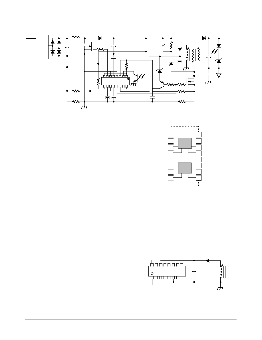
OPERATING DESCRIPTION
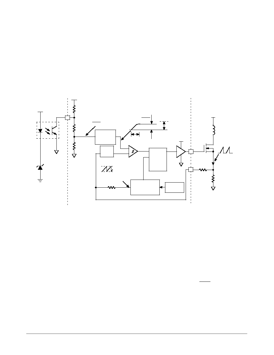
Figure 45. Typical Application Circuit
EMI
Filter
NCP1603
+
-
V
ac
Z
OVP
V
out
V
in
L
I
L
D
1
C
filter
Q
1
R
S1
R
CS1
C
bulk
C
osc
R
FB1
I
FB1
I
S
C
control
C
ramp
R
CS2
R
S2
V
bulk
R
FF
I
D
D
3
Q
2
D
2
C
out
C
s
Z
ref
Introduction
The NCP1603 is a PWM/PFC combo controller for
two-stages PFC low-power application. A typical
application circuit is listed in Figure 45. The first-stage PFC
boost circuit draws a near-unity power factor current from the
input but it also steps up the rectified input voltage V
in
to a
high bulk voltage V
bulk
in the bulk capacitor C
bulk
. Then, the
second-stage PWM flyback circuit converts the bulk voltage
V
bulk
to a usable low voltage and isolated output voltage V
out
.
The controllers of the two stages are combined to become a
single PWM/PFC combo controller. The advantages of
NCP1603 are the following:
1. Integrated maximum 500 V lossless high voltage
startup circuit that saves area and power loss.
2. Low standby power consumption because of PFC
shutdown and skipping cycle operation.
3. Proprietary PFC methodology limits the
maximum switching frequency and frequency
jittering feature of the second-stage make the
easier front-ended EMI filter design.
4. Internal ramp compensation for stability
improvement in the second stage converter.
5. Minimum number of external components.
6. Optional synchronization capability between the
PFC and PWM sections for bulk capacitor ripple
current reduction.
7. Safety protection features.
NCP1603 is a co-package of two individual IC dies.
(NCP1601 and NCP1230, 100 kHz) The PFC die links up
pin 5 to pin 12 that are in the lower half of Figure 46. The
PWM die links up the other pins that are in the upper half
of Figure 46. For simplicity, the PFC pins are named with
suffix one that stands for the first stage and the PWM pins
are named with suffix two that stands for the second stage.
This dual-dies architecture allows the PFC die to be
completely powered off in the standby low-power
condition. It makes the power supply an excellent
low-power no load standby performance.
16
15
14
12
11
10
9
HV
NC
Ramp
CS1
FB1
V
CC2
V
control
13 Out2
1
2
3
4
5
6
7
8
Osc
FB2
CS2
GND2
GND1
Out1
V
CC1
V
aux
PWM
Die
PFC
Die
Figure 46. Internal Connection
Biasing the Controller
The PWM section is the master section that always
operates. The PFC section is the slave section that is
powered off in standby condition for power saving. It is
implemented by connecting V
aux
pin (Pin 1) and V
CC1
pin
(Pin 8) together externally. The V
CC1
pin generally
requires a small decoupling external capacitor (0.1
mF) or
nothing. The PWM section powers the PFC section. The
V
CC
of the whole device refers to V
CC2
(Pin 14) in the
PWM section (i.e., V
CC
= V
CC2
).
Figure 47. Bias Supply Schematic
NCP1603
16
14
1
4
6
8
V
bulk
V
CC2
C
VCC
GND1 = GND2
V
CC1
= V
aux
NCP1603
http://onsemi.com
17
The recommended biasing schematic of the controller is in
Figure 47 while a typical completed application schematic
can be referred to Figure 45. These two dies have their own
individual supply voltages at Pin 8 and Pin 14. The grounds
of the two dies are physically connected through the package
substrate but they are needed to be connected externally. The
bias voltage to the NCP1603 comes from the bulk voltage
V
bulk
through the HV pin (Pin 16) during startup. After
startup, a second-stage flyback transformer auxiliary winding
delivers the supply voltage to V
CC
.
Lossless High Voltage Startup Circuit
Figure 48. V
CC2
Management
Q S
R
Double
Hiccup
B
2
Counter
&
Turn Off
+
-
UVLO
3.2 mA
16
V
bulk
HV
12.6/
5.6 V
+
-
7.7 V
20 V
14
V
CC
Turn on Internal Bias
The HV pin (Pin 16) is capable of the maximum 500 V so
that this pin can be directly connected to the bulk voltage
V
bulk
and delivers startup supply voltage to the controller.
Figure 48 illustrates the block diagram of the startup circuit.
An UVLO comparator monitors the V
CC
at Pin 14. A startup
current source is activated and deactivated whenever the
voltage reaches V
CC2(latch)
(5.6 V typical) and V
CC2(on)
(12.6 V typical) thresholds respectively. Therefore, the V
CC
never drops below V
CC2(latch)
after powering up unless the
circuit is unplugged (i.e., V
bulk
disappears or smaller than its
minimum required operating threshold V
start(min)
(20 V
typical)). This feature makes the controller memorize the
external latch off function implemented in Pin 3.
This in-chip startup circuit can minimize the number of
external components and Printed Circuit Board (PCB) area.
It also minimizes the loss due to startup resistor because
startup resistor always dissipates power but this startup circuit
can be turned off when the V
CC
voltage is sufficient. Actually,
there is a small leakage current I
HV3
(30
mA typical at
HV = 700 V) when the startup circuit is off.
The V
CC
capacitor is recommended to be at least 47
mF to
ensure that V
CC
is always above the minimum operating
voltage V
CC2(off)
(7.7 V typical) in the startup phase. For
example, the PWM die consumes I
CC2(op2)
(2.2 mA typical),
a 47
mF V
CC
capacitor can maintain the V
CC
above 7.7 V for
105 ms. It is the available time to establish a V
CC
voltage
from the flyback transformer auxiliary winding.
tstartup
+
CVCC
D
V
ICC2(op2)
+
47
m
F∑(12.6 V-7.7 V)
2.2 mA
+
105 ms
(eq. 1)
A large enough V
CC
capacitor can also help to maintain
V
CC2
always above V
CC2(off)
to prevent the IC accidentally
powered off during the standby condition where the
low-frequency ripple of V
CC2
can be very high.
The PFC section does not consume any current in the
startup phase since V
aux
is disabled initially (i.e., V
aux
=
V
CC1
= 0 V).
When V
CC2
falls below V
CC2(off)
(7.7 V typical) for
whatever reason, the PWM section sleeps and it consumes
I
CC2(latch)
(680
mA typical) until V
CC2
reaches V
CC2(latch)
(5.6 V typical). When V
CC2
reaches V
CC2(latch)
(5.6 V
typical), the startup current source activates and V
CC2
rises
again.
Figure 49. V
aux
Enabled Regions
0.75 V
3.0 V
Non-
usable
Vaux
Enabled
Region
V
FB2
Fault Condition (V
FB2
> 3.0 V)
Usable
Vaux
Enabled
Region
Standby Condition (V
FB2
< 0.75 V)
7.7 V
V
CC2
(PWM)
18 V
12.6 V
V
CC1
(PFC)
18 V
10.5 V
9.0 V
Auxiliary Supply V
aux
The V
aux
pin (Pin 1) connects to the V
CC1
pin (Pin 8)
externally. Internally, the V
aux
pin is connected to V
CC2
through an internal MOSFET. The MOSFET on-resistance
is R
aux
(11.7
W typical). It delivers a supply voltage from
the PWM section to the PFC section. The V
aux
is disabled
when one of the following conditions occurs.
1. V
aux
is initially disabled because of no feedback
signal (V
FB2
> 3.0 V) initially.
2. Fault condition (V
FB2
> 3.0 V for more than
125 ms).
3. Standby condition (V
FB2
< V
stby
(0.75 V typical)
and then V
FB2
< V
stby-out
(1.25 V typical) for
more than 125 ms).
4. Insufficient operating supply voltage (V
CC2
<
V
CC2(off)
(7.7 V typical)).
5. Overvoltage protection (OVP) latch activated from
CS2 pin (Pin 3) (V
CS2
> V
OVP
(3.0 V typical)).
6. Thermal shutdown latch in the PWM section
activated when the junction temperature is over
typical 150
_C.
NCP1603
http://onsemi.com
18
The UVLO start thresholds of V
CC1
is V
CC1(on)
(10.5 V
typical) and the maximum allowable limit is 18 V. On the
other hand, the V
aux
is enabled when V
CC2
is over V
CC2(off)
(7.7 V typical). Hence, there are two possible operating
regions in Figure 49. In the non-usable region the V
aux
is
not high enough to turn on the PFC section. Therefore, the
flyback transformer auxiliary winding must be between
V
CC1(on)
(10.5 V typical) and 18 V.
Regulation in the PWM Section
The PWM section (or the second stage) of the NCP1603
is NCP1230 that is a current-mode fixed-frequency PWM
flyback controller with internal compensation ramp. The
simplified block diagram of the duty cycle regulation
section is in Figure 50. A 100 kHz clock oscillator is
modulated by adding a frequency jittering feature. This
modulated 100 kHz clock signal turns the Out2 (pin 13)
high in each switching cycle. The Out2 goes low when the
current-loop feedback signal intersects with the output
voltage-loop feedback signal. A duty cycle is therefore
generated. The maximum duty ratio is limited to D
max
(80% typical).
V
out
2
Opto
Coupler
FB2
Vdd
20 k
55 k
25 k
V
FB2
V
FB2
3
Soft-Start
Processing
Circuit
-
+
200 ns
LEB
Soft-Start Period 2.5 ms
V
FB2
3
1 V Max
PWM
R
S
Q
Max Duty
= 80%
V
CC2
13
3
Out2
V
bulk
Flyback
Drain
Current
I
D
CS2
R
S2
R
CS2
6.4% Frequency
Jittering
Modulation
100 kHz
Oscillator
2.3 V
0 V
100 kHz
Jittering Ramp
18 k
Figure 50. Block Diagram of Duty Cycle Regulation in the PWM Section
The current-loop feedback circuit consists of a typical
200 ns Leading Edge Blanking (LEB) that is to prevent a
premature reset of the output due to noise, a pair of sense
resistors R
CS2
and R
S2
that sense the flyback drain current
I
D
, and a 0-to-2.3 V jittering ramp that adds a ramp
compensation for a stability improvement to the
current-mode control possibly in continuous mode
operation.
The V
FB2
is approximately divided by 3 by an internal
pair of resistors (55 k
W and 25 kW). The soft-start
processing circuit reduces the initial voltage-loop
feedback signal (V
FB2
/ 3) for 2.5 ms. After this 2.5 ms, the
soft-start disappears. As a result, the startup envelope of
the peak drain current (or duty ratio) ramps up gradually for
2.5 ms. It is noted that the 2.5 ms is counted when the PWM
die circuit is reset that is when V
CC2
reaches V
CC2(on)
(12.6 V typical). This soft-start feature offers a reduced
transient voltage and current stress on the power circuit
during the startup.
Excessive output voltage causes more the optocoupler
current. It pulls down the V
FB2
through FB2 pin (Pin 2) and
generates a lower duty ratio. The output voltage reduces.
Insufficient output voltage reduces the optocoupler
current. If the current is too small, the V
FB2
is eventually
pulled high than 3.0 V (3.8 V typical). The (V
FB2
/3) signal
is then clamped to an internal 1.0 V limit. If the ramp is
ignored (i.e., R
S2
= 0), the maximum possible drain current
is derived as:
ID(max)
+
1 V
RCS2
(eq. 2)
It is noted that resistor R
S2
will affect the percentage of
the ramp getting compared for the modulation. Hence, a
large value of the R
S2
increase the ramp and will reduce the
possible maximum duty ratio.

NCP1603
http://onsemi.com
19
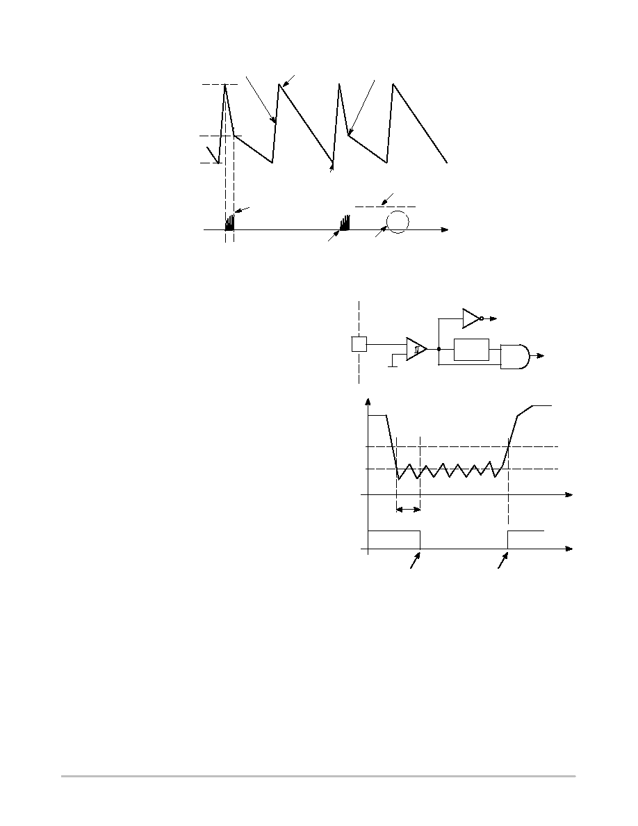
Frequency Jittering
93.6 kHz
100 kHz
106.4 kHz
5 ms
time
PWM Section Oscillator Frequency
Figure 51. Frequency Jittering of PWM Oscillator
Frequency jittering is a method used to soften the EMI
signature by spreading the energy in the vicinity of the main
switching component. The PWM Section offers a typical
±6.4% deviation on the nominal switching frequency
(100 kHz typical). A sweep sawtooth modulates the
100 kHz clock up and down with a 5.0 ms period.
Figure 51 illustrates the
±6.4% variation of the jittering
oscillator frequency versus time.
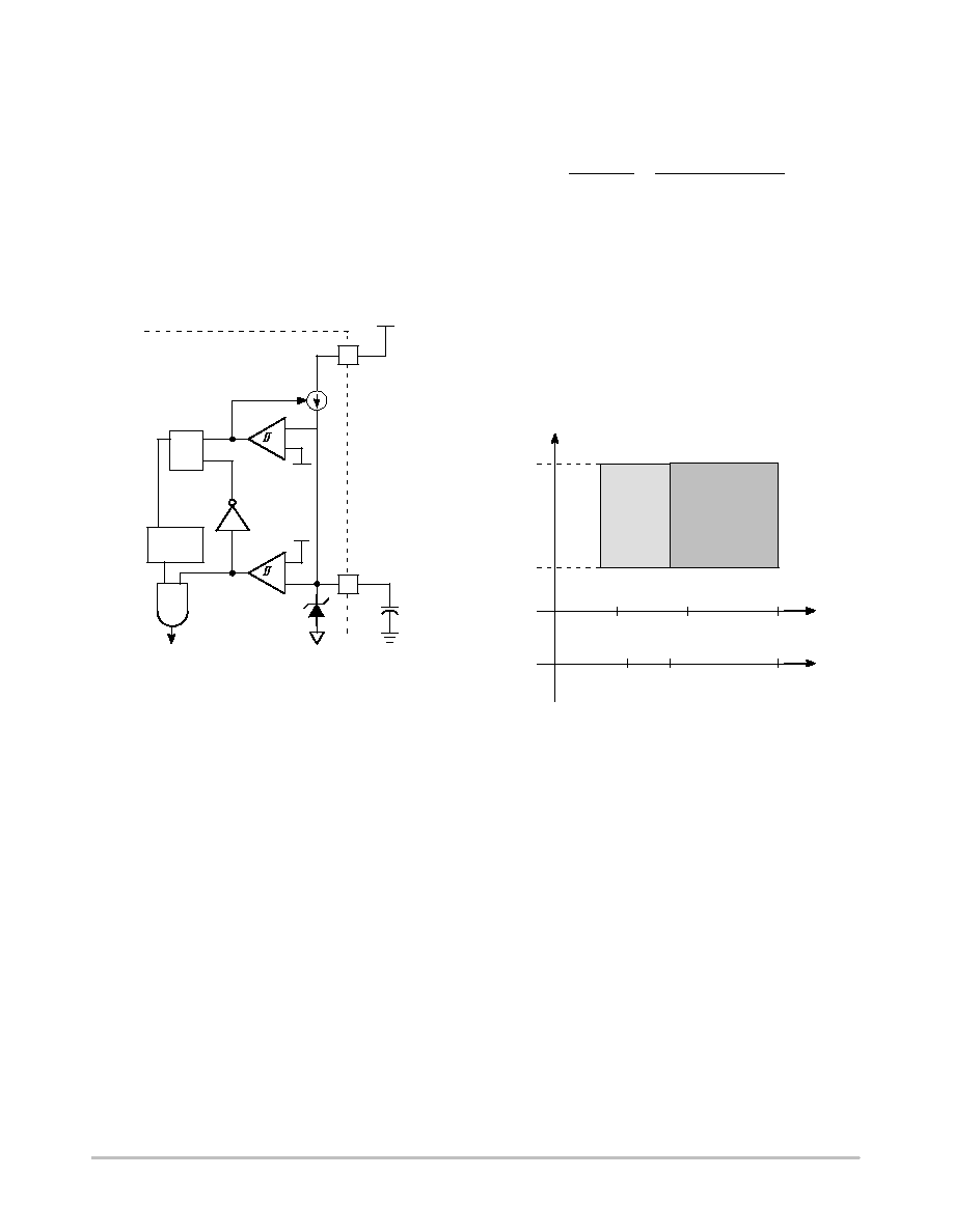
Fault Condition
Figure 52 illustrates the fault detection circuitry and its
timing diagram. When fault (or output short circuit)
happens, the output voltage collapses and the optocoupler
is opened. V
FB2
is internally pulled to be higher than 3.0 V
(3.8 V typical). Then, the controller activates an error flag
when (V
FB2
/3) is greater than the soft-start voltage V
SS
that is 1.0 V after the 2.5 ms from startup.
When the circuit is powering up in the beginning, the
output voltage is not yet established and FB2 pin (Pin 2) is
opened. Therefore, there is a 125 ms timer to allow the
circuit to establish an initial output voltage. Then, a fault
(or short circuit) condition is recognized when an error flag
(V
FB2
q 3.0 V) can last for 125 ms. When a fault is
detected, Out2 (Pin 13) goes low. The power supply stops
delivering power to the output. On the other hand, the V
aux
(= V
CC1
) also goes low. The V
aux
will restore immediately
when the error flag disappears.
This fault detection method offers advantage of getting
rid of the auxiliary winding information that cannot truely
represent the output voltage when the flyback transformer
is badly coupled.
-
+
2
FB2
Vdd
20 k
55 k
25 k
V
FB2
V
FB2
3
Soft-Start
1 V Max
V
SS
Start Vaux
Enable Vaux/PFC
125 ms
Delay
&
Fault
Disable
Vaux/PFC
and Out2
Soft-Start Period 2.5 ms
Figure 52. Block Diagram and Timing Diagram of Fault Detection
1 V
V
FB2
/3
V
SS
V
aux
125ms
V
aux
starts when V
FB2
is
within regulation window
(V
FB2
< 3 V).
(i.e., normal operation)
V
aux
stops when V
FB2
is out of
regulation window (V
FB2
> 3 V)
for more than 125 ms.
(i.e., fault condition)
1 V
time
time
NCP1603
http://onsemi.com
20
5.6 V
12.6 V
7.7 V
0A
V
CC2
I
D
Startup current source
charging the V
CC
capacitor
Startup circuit turns off
when V
CC2
is 12.6 V
Circuit sleeps when
V
CC2
is below 7.7 V
Maximum drain current
is limited to 1 / R
CS2
Startup circuit turns on
when V
CC2
is 5.6 V
Switching starts when
V
CC2
reaches 12.6 V
Peak drain current follows
a 2.5 ms soft-start envelope
Switching is missing
in every two V
CC
hiccup cycles
featuring a "double hiccup"
Figure 53. Timing Diagram of Fault Condition
time
Figure 53 illustrates the timing diagram of V
CC2
and the
second-stage drain current I
D
in fault condition. The V
CC
drops because output voltage collapses. When V
CC
drops
below V
CC(off)
(7.7 V typical), the Drive Output signal
disappears and the V
CC
continues to drop. When bias
voltage V
CC
drops to V
CC(latch)
(5.6 V typical), the startup
current source activates and charge up the V
CC
until V
CC
reaches V
CC(on)
(12.6 V typical). The internal 2.5 ms
soft-start activates after V
CC
reaches V
CC(on)
(12.6 V
typical). The peak drain current follows its 2.5 ms
envelope. The power supply dissipates some power due to
the switching signal of Out2 and waits for possible
auto-recovery of operation when the fault is cleared.
As shown in Figure 53, NCP1603 has a "double hiccup"
feature that allows the drain current in every two V
CC
hiccup cycle in fault condition. The "double hiccup"
feature offers fewer power dissipation during fault
condition comparing to "single hiccup".
If the fault is cleared (V
FB2
< 3.0 V
SS
) and V
CC
remains
above V
CC2(off)
(7.7 V typical), the circuit will resume its
operation. Otherwise, the V
CC
will continue this
12.6-7.7-5.6-12.6 V hiccup mode until the fault or bulk
voltage is cleared.
Standby Condition
The output voltage rises up excessively in standby
condition and the V
FB2
drops. A set point of 25% of the
maximum of V
FB2
(i.e., 3.0 V) is defined to be the standby
threshold. Hence, the standby threshold is V
stby
= 25%
◊
3.0 V = 0.75 V.
FB2
125 ms
delay
&
Leave standby
-
+
2
0.75 V / 1.25 V
VFB2
enable Vaux /
Standby
disable
Vaux/
PFC
Section
Figure 54. Block Diagram and Timing Diagram of
Standby Detection
V
FB2
V
aux
1.25 V
0.75 V
125 ms
V
aux
stops when V
FB2
is
below 0.75 V and cannot go
above 1.25 V for 125 ms
V
aux
restores when
V
FB2
goes above 1.25 V
time
time
PFC Section

NCP1603
http://onsemi.com
21
Figure 54 illustrates the standby detection circuitry and
its timing diagram. When standby condition happens (i.e.,
V
FB2
< 0.75 V), the controller will wait for a typical 125 ms
to ensure that the output power remains low for a while.
Then, the V
aux
is disabled to shut down the PFC section for
power saving. The V
aux
(or the PFC) restores when V
FB2
goes above 1.25 V immediately because V
FB2
can be
possibly above the 0.75 V threshold during standby
operation (referring to Figure 55) and the PFC section is
needed after the circuit restores from standby condition.
Figure 55. Timing Diagram in Standby Condition
V
CC2
V
FB2
I
D
Out2 goes low (no drain current) when V
FB2
< 0.75 V
V
CC2
needs to be above 7.7 V to ensure
proper operation of the controller and
main output within regulation
1.25 V
0.75 V
7.7 V
time
Figure 56. Block Diagram in Standby Operation in
PWM Section
CS2
FB2
Vcc2
Out2
PWM
R
S
-
+
2
3
13
clock
0.75 V
+
-
OR
Standby
Q
V
FB2
Figure 55 and 56 show the timing diagram and block
diagram of the standby operation respectively. A skipping
cycle behavior of the drain current is made by reset the
latch whenever V
FB2
is smaller than 0.75 V. When V
FB2
is
greater than 0.75 V, the duty ratio is modulated by the
PWM block that is illustrated in Figure 50.
PFC in Discontinuous/Critical Mode
The PFC section of the NCP1603 is NCP1601 that is
designed for low-power PFC boost circuit in DCM or CRM
and takes advantages on both operating modes. DCM limits
the maximum switching frequency. It simplifies the
front-ended EMI filter design. CRM limits the maximum
currents of diode, MOSFET and inductor. It reduces the
costs and improves the reliability of the circuit. This device
substantially exhibits unity power factor while operating in
DCM and CRM. It minimizes the number of external
components.
The PFC section primarily designed to operate in
fixed-frequency DCM. In the most stressful conditions,
CRM can be an alternative option that is without power
factor degradation. On the other hand, the PFC section can
be viewed as a CRM controller with a frequency clamp
(maximum switching frequency limit) alternative option
that is also without power factor degradation. In summary,
the PFC section can cover both CRM and DCM without
power factor degradation. Based on the selections of the
boost inductor and the oscillator frequency, the circuit is
capable of the following three applications.
1. CRM only by setting the oscillator frequency
higher than the CRM frequency range.
2. CRM and DCM by setting the oscillator
frequency somewhere within the CRM frequency
range.
3. DCM only by setting the oscillator frequency
lower than the CRM frequency range.
Figure 57. Timing Diagram of the PFC Stage
critical mode
DCM
DCM
time
current
time
time
time
V
in
V
ton
V
control
Inductor current, I
L
Input current, I
in

NCP1603
http://onsemi.com
22
DCM needs higher peak inductor current comparing to
CRM in the same averaged input current. Hence, CRM is
generally preferred at around the sinusoidal peak for lower
the maximum current stress but DCM is also preferred at
the non-peak region to avoid excessive switching
frequencies. Because of the variable-frequency feature of
the CRM and constant-frequency feature of DCM,
switching frequency is the maximum in the DCM region
and hence the minimum switching frequency will be found
at the moment of the sinusoidal peak.
DCM PFC Circuit
A DCM/CRM PFC boost converter is shown in
Figure 58. Input voltage is a rectified 50 or 60 Hz
sinusoidal signal. The MOSFET is switching at a high
frequency (typically around 100 kHz) so that the inductor
current I
L
basically consists of high-frequency and
low-frequency components.
Figure 58. DCM/CRM PFC Boost Converter
V
in
I
in
I
L
L
V
out
C
bulk
C
filter
Filter capacitor C
filter
is an essential and very small value
capacitor in order to eliminate the high-frequency content
of the DCM inductor current I
L
. This filter capacitor cannot
be too bulky because it can pollute the power factor by
distorting of the rectified sinusoidal input voltage.
PFC Methodology
The PFC section uses a proprietary PFC methodology
particularly designed for both DCM and CRM operation.
The PFC methodology is described in this section.
Figure 59. Inductor Current in DCM
t
1
t
2
t
3
I
pk
T
time
Inductor Current
As shown in Figure 59, the inductor current I
L
of each
switching cycle starts from zero in DCM. CRM is a special
case of DCM when t
3
= 0. When the PFC boost converter
MOSFET is on, the inductor current I
L
increases from zero
to I
pk
for a time duration t
1
with inductance L and input
voltage V
in
. Equation 3 is formulated.
Vin
+
L
Ipk
t1
(eq. 3)
The input filter capacitor C
filter
and the front-ended EMI
filter absorb the high-frequency component of inductor
current. It makes the input current I
in
a low-frequency
signal.
Iin
+
Ipk (t1
)
t2)
2 T
for DCM
(eq. 4)
Iin
+
Ipk
2
for CRM
(eq. 5)
From Equations 3, 4, and 5, the input impedance Z
in
is
formulated.
Zin
+
Vin
Iin
+
2TL
t1(t1
)
t2)
for DCM
(eq. 6)
Zin
+
Vin
Iin
+
2L
t1
for CRM
(eq. 7)
Power factor is corrected when the input impedance Z
in
in Equations 6 and 7 are constant or slowly varying.
Figure 60. PFC Modulation Circuit and Timing
Diagram
-
+
closed when
output low
Turns off
MOSFET
Ramp
12
C
ramp
I
ch
V
ton
V
ton
ramp
out1
PWM
Comparator
The MOSFET on time t
1
of PFC modulation duty is
generated by a feedback signal V
ton
and a ramp. The PFC
modulation circuit and timing diagram are shown in
Figure 60. A relationship in Equation 8 is obtained.
t1
+
Cramp Vton
Ich
(eq. 8)
The charging current I
ch
is constant 100
mA current and
the ramp capacitor C
ramp
is constant for a particular design.
Hence, according to Equation 8, the MOSFET on time t
1
is proportional to V
ton
.
In order to protect the PFC modulation comparator, the
maximum voltage of V
ton
is limited to internal clamp
V
ton(max)
(3.9 V typical) and the ramp pin (Pin 12) is with
NCP1603
http://onsemi.com
23
a 9.0 V ESD zener diode. The 3.9 V maximum limit of this
V
ton
indirectly limits the maximum on time.
The V
control
processing circuit generates V
ton
from
control voltage V
control
and time information of zero
inductor current. The circuit in Figure 61 makes
Equations 9 and 10 where the value of resistor R
1
is much
higher than the value of resistor R
2
(R
1
>> R
2
).
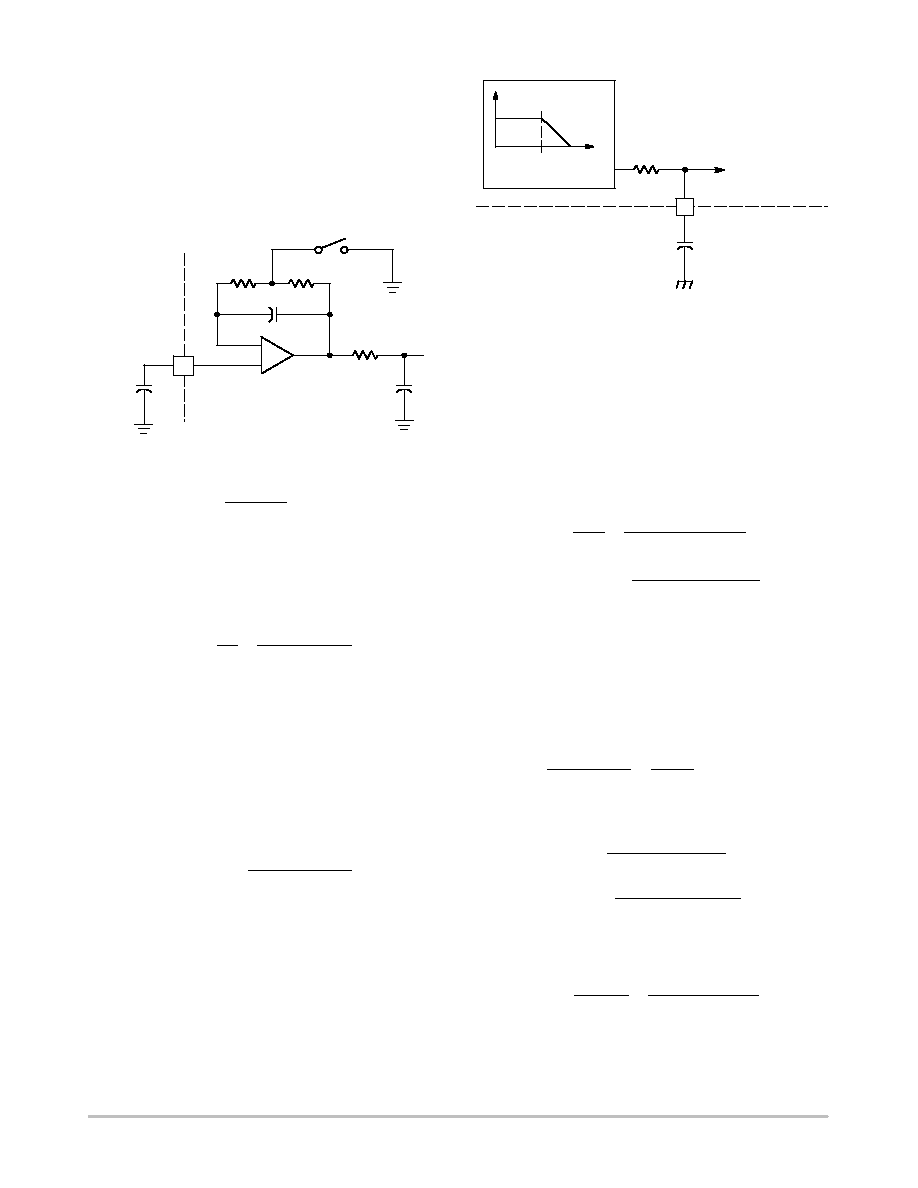
Figure 61. V
control
Processing Circuit
+
-
closed when zero current
10
C
control
V
control
R
1
R
2
R
3
C
1
C
3
V
ton
Vton
+
T Vcontrol
t1
)
t2
for DCM
(eq. 9)
Vton
+
Vcontrol for CRM
(eq. 10)
It is noted that V
ton
is always greater than or equal to
V
control
(V
ton
q V
control
).
In summary, the input impedance Z
in
in Equation 11 is
obtained from Equations 3 through 10.
Zin
+
Vin
Iin
+
2LIch
Cramp Vcontrol
(eq. 11)
Control voltage V
control
comes from the PFC boost
circuit output voltage (i.e., bulk voltage V
bulk
) that is a
slowly varying signal. The bandwidth of V
control
can be
additionally limited by inserting an external capacitor
C
control
to the V
control
pin (Pin 10) in Figure 62. The
internal 300 k
W resistor and the capacitor C
control
create a
low-pass filter that has a bandwidth f
control
in Equation 12.
It is generally recommended to limit the bandwidth below
20 Hz to achieve power factor correction. Typical value of
C
control
is 0.1
mF.
Ccontrol
u
1
2
p
300k
W
fcontrol
(eq. 12)
Figure 62. V
control
Low-Pass Filtering
300k
Regulation Block
10
C
control
V
control
V
reg
I
ref
I
ref
96%
I
FB1
V
control
Processing
Circuit
If the bandwidth of V
control
is much less than the 50 or
60 Hz line frequency, the input impedance Z
in
is slowly
varying or roughly constant. Then, the power factor
correction is achieved in DCM and CRM.
Maximum Power in PFC Section
Input and output power (P
in
and P
out
) are derived in
Equations 13 and 14 when the circuit efficiency
is
obtained or assumed. The variable V
ac
stands for the RMS
input voltage.
Pin
+
Vac2
Zin
+
Vac2CrampVcontrol
2LIch
(eq. 13)
Pout
+ h
Pin
+
h
Vac2CrampVcontrol
2LIch
(eq. 14)
From Equations 13 and 14, control voltage V
control
controls the amount of output power, input power, or input
impedance. The maximum value of the control voltage
V
control
is 1.05 V (i.e., V
control(max)
= 1.05 V). A parameter
called maximum power resistor R
power
(10.5 k
W typical) is
defined in Equation 18 and restricted to have a maximum
±10% variation (i.e., 9.5 kW p R
power
p 11.5 kW) for
defining the maximum power in an application.
Rpower
+
Vcontrol(max)
Ich
+
1.05 V
100
m
A
+
10.5 k
W
(eq. 15)
It means that the maximum input and output power
(P
in(max)
and P
out(max)
) are limited to
±10% variation.
Pin(max)
+
Vac2CrampRpower
2 L
(eq. 16)
Pout(max)
+
h
Vac2CrampRpower
2 L
(eq. 17)
The maximum input current I
ac(max)
to deliver the
maximum input power P
in(max)
is also derived in (eq.14).
The suffix ac stands for RMS value.
Iac(max)
+
Pin(max)
Vac
+
VacCrampRpower
2 L
(eq. 18)

NCP1603
http://onsemi.com
24
Feedback in PFC Section
The output voltage of the PFC circuit (i.e., bulk voltage
V
bulk
) is sensed as a feedback current I
FB1
flowing into the
FB1 pin (Pin 9) of NCP1603. The FB1 pin voltage V
FB1
is
typically smaller than 5.0 V referring to Figure 31. It is
much lower than V
bulk
that is typically 400 V. Therefore,
V
FB1
is generally neglected.
IFB1
+
Vbulk
*
VFB1
RFB1
[
Vbulk
RFB1
(eq. 19)
where R
FB1
is the feedback resistor connected the FB1 pin
(Pin 9) and the output voltage referring to Figure 45.
Then, the feedback current I
FB1
represents the bulk
voltage V
bulk
and will be used in the PFC section voltage
regulation, undervoltage protection (UVP), and
overvoltage protection (OVP).
Bulk Voltage Regulation in PFC Section
PFC-stage feedback current I
FB1
, that presents bulk
voltage V
bulk
or the PFC-stage output voltage, is regulated
with a reference current (I
ref
= 203
mA typical) as shown in
Figure 63. When I
FB1
is lower than 96% of I
ref
, the V
reg
that
is the output of the regulation block is as high as
V
control(max)
(1.05 V typical) that it gives the maximum
value on V
ton
and the maximum MOSFET on time and
V
bulk
increases. When I
FB1
is higher than I
ref
, the V
reg
becomes 0 V that gives no MOSFET on time and V
bulk
decreases. As a result, the bulk voltage V
bulk
is regulated
around the range between 96% and 100% of the nominal
value of R
FB1
◊ I
ref
.
Figure 63. Regulation Block
V
reg
I
ref
I
ref
96%
I
FB1
1 V
Based on Equations 13 and 14 for a particular power
level, the V
control
is inversely proportional to V
ac
2
. Hence,
in high V
ac
condition V
control
is lower. It means that I
FB1
or
output voltage is higher based on the regulation block
characteristic in Figure 63. In other words, the V
control
in
the low V
ac
condition is much higher than the high V
ac
condition. In order to not over-design the circuit in the
application, the V
control
in the low V
ac
condition is usually
very closed to V
control(max)
. It makes the output voltage be
almost 96% of the nominal value of R
FB1
◊ I
ref
in high V
ac
condition.
The feedback resistor R
FB1
consists of two or three high
precision resistors in order to set the nominal V
bulk
precisely and for safety purpose.
The regulation block output V
reg
is connected to control
voltage V
control
through an internal resistor R
control
(300 k
W typical) for the low-pass filter in Figure 62. The
V
control
and the time information of zero current are
collected in the V
control
processing circuit to generate V
ton
that is then compared to a ramp signal to generate the
MOSFET on time t
1
for power factor correction.
Current Sense in PFC Section
The PFC section senses the inductor current I
L
by the
current sense scheme in Figure 64. This scheme has the
advantages of: (1) the inrush current limitation by the
resistor. R
CS1
. and (2) the overcurrent protection and zero
current detection implemented in the same pin.
Figure 64. Current Sense in PFC Section
CS1
NCP1603
Gnd1
+
-
R
CS1
R
S1
I
L
I
S
I
L
V
S
Inductor current I
L
passes through R
CS1
and creates a
negative voltage. This voltage is measured by a current I
S
flowing out of the CS1 pin (Pin 11). CS1 pin has an offset
voltage V
S
. This offset voltage is studied in the setting of
zero inductor current I
L(ZCD)
and the maximum inductor
current I
L(OCP)
(i.e., overcurrent protection threshold). A
typical variation of offset voltage V
S
versus sense current
I
S
is shown in Figure 35. Based on Figure 64, Equation 20
is derived.
VS
*
RS1 IS
+
-RCS1 IL
(eq. 20)
Zero Current Detection (ZCD) in PFC Section
The device recognizes zero inductor current when CS1
pin (Pin 11) sense current I
S
is smaller than I
S(ZCD)
(14
mA
typical). The offset voltage of the CS1 pin in this condition
is V
S(ZCD)
(7.5 mV typical). The inductor current I
L(ZCD)
at the ZCD condition is derived in Equation 21.
IL(ZCD)
+
RS1IS(ZCD)
*
VS(ZCD)
RCS1
(eq. 21)

NCP1603
http://onsemi.com
25
It is obvious that the I
L(ZCD)
is not always zero. In order
to make it reasonably close to zero, the setting of R
S1
and
R
CS1
are crucial.
Figure 65. CS Pin Characteristic when I
L
= 0
I
S(ZCD)
V
S(ZCD)
R
S1
> R
S(ZCD)
R
S1
= R
S(ZCD)
V
S
Operating ZCD point
Ideal ZCD point
I
S
Based on the CS pin (Pin 4) characteristics in Figure 35,
Figure 65 is studied here. When the inductor current is
exactly zero (i.e., I
L(ZCD)
= 0), the ideal ZCD point in the
Figure 65 is reached where R
S1
is R
S(ZCD)
(536
W typical).
Considering the tolerance, the actual sense resistor R
S1
is
needed to be higher than the ideal value of R
S(ZCD)
to
ensure that zero current signal is generated when sense
current is smaller than the ZCD threshold (i.e., I
S
<
I
S(ZCD)
). That is,
RS
u
RS(ZCD)
+
VS(ZCD)
IS(ZCD)
(eq. 22)
The higher value of R
S1
makes the bigger distance
between the operating and ideal ZCD points in Figure 65.
Hence, R
S1
has to be as low value as possible. The best
recommended value of R
S1
is therefore the maximum of
R
S(ZCD)
that is 1.0 k
W.
Now that the R
S1
is set at a particular value that is greater
than R
S(ZCD)
. From Equation 20, the operating lines in
Equation
23 with different inductor currents I
L
of
Equation 20 are studied.
VS
+
RS1IS
*
RCS1IL
(eq. 23)
These operating lines are added in Figure 65 to formulate
Figure 66. When the inductor current I
L
is smaller than
I
L(ZCD)
, the sense current I
S
is smaller than I
S(ZCD)
and
hence the zero current signal is generated.
Figure 66. CS Pin Characteristic with Different
Inductor Current
I
S(ZCD)
V
S(ZCD)
V
S
Operating
ZCD point
I
S
Best
ZCD
point
I
L
= I
L(ZCD)
I
L
> I
L(ZCD)
I
L
= 0
It is noted in Figure 66 and Equation 23 that when the
(R
CS1
I
L
) term is smaller the error or distance between the
lines to the line I
L
= 0 is smaller. Therefore, the value of the
current sense resistor R
CS1
is also recommended to be as
small as possible to minimize the error in the zero current
detection.
Overcurrent Protection (OCP) in PFC Section
Overcurrent protection is reached when I
S
is larger than
I
S(OCP)
(200
mA typical). The offset voltage of the CS pin
is V
S(OCP)
(3.2 mV typical) in this condition. That is:
IL(OCP)
+
RS1IS(OCP)
*
VS(OCP)
RCS1
(eq. 24)
When overcurrent protection threshold is reached, the
Drive Output of the device goes low.
Oscillator/Synchronization Block in PFC Section
Figure 67. Oscillator / Synchronization Block
in PFC Section
Oscillator Clock
S
R
Q
Zero Current
Turn on
MOSFET
-
+
5 V/3.5 V
Osc
delay
0
5
1
45
m
A
94
m
A
&

NCP1603
http://onsemi.com
26
The PFC section is designed to operate in either DCM or
CRM. In order to keep the operation in DCM and CRM
only, the Drive Output cannot turn on as long as there is
some inductor current flowing through the circuit. Hence,
the zero current signal is provided to the oscillator/
synchronization block in Figure 67. An input comparator
monitors the Osc pin (Pin 5) voltage and generates a clock
signal. The negative edge of the clock signal is stored in a
RS latch. When zero current is detected, the RS latch will
be reset and a set signal is sent to the output drive latch that
turns on the MOSFET in the PFC boost circuit. Figure 68
illustrates a typical timing diagram of the oscillator block.
Figure 68. Oscillator Block Timing Diagram
time
clock
inductor
clock latch
(latch set signal)
Discontinuous mode
Critical mode
(latch output)
current
clock edge
Oscillator Mode in PFC Section
In oscillator mode, the Osc pin (Pin 5) is connected to an
external capacitor C
osc
. When the voltage of this pin is above
V
sync(H)
(5.0 V typical), the pin sinks a current I
odch
(94≠45
= 49
mA typical) and the external capacitor C
osc
discharges.
When the voltage reaches V
sync(L)
(3.5 V typical), the pin
sources a current I
och
(45
mA typical) and the external
capacitor C
osc
is charged. It is noted that there is a typical
300 ns propagation delay and the 3.5 V and 5.0 V threshold
conditions are measured on 220 pF C
osc
capacitor. Hence, the
actual oscillator hysteresis is a little bit smaller.
Figure 69. Oscillator Mode Timing Diagram in DCM
Osc pin
voltage
Osc clock
Clock edge
Drive output
(DCM)
5 V
3.5 V
There is an internal capacitance C
osc(int)
(36 pF typical)
in the oscillator pin and the oscillator frequency is to
f
osc(max)
(405 kHz typical) when the Osc pin is opened.
Hence, the oscillator switching frequency can be
formulated in Equation 25 and represented in Figure 70.
Cosc
+
36 pF
@
405 kHz
fosc
*
36 pF
(eq. 25)
0
100
200
300
400
500
600
700
0
50
100
150
200
f
osc
, Oscillator Frequency (kHz)
C
osc
, Oscillator Capacitor (pF)
Figure 70. Osc Pin Frequency Setting
Synchronization Option
In synchronization mode, the Osc pin (Pin 5) receives an
external digital signal with level high defined to be higher
than V
sync(H)
(5.0 V typical) and level low defined to be
lower than V
sync(L)
(3.5 V typical). An internal 9.0 V ESD
Zener diode is connected to the Osc pin and hence the
maximum allowable synchronization voltage is 9.0 V. The
circuit recognizes a synchronization frequency by the time
difference between two falling edge instants when the
synchronization signal across the 3.5 V threshold point.
The actual synchronization threshold point is a little bit
higher than the 3.5 V threshold point. The minimum
synchronization pulse width is 500 ns.
There is a typical 350
ns propagation delay from
synchronization threshold point to the moment of output goes
high and there is also a typical 300 ns propagation delay from
the synchronization threshold point to the moment of crossing
3.5 V. Hence, the output goes high apparently when the sync
signal turns to 3.5 V. A timing diagram of synchronization
mode is summarized in Figure 71.
Figure 71. Synchronization Mode Timing Diagram in
DCM
Sync Signal
Osc Clock
Clock Edge
Drive Output
(DCM)
5 V
3.5 V
The PWM and PFC Section can be synchronized
together in order to minimize some of the ripple current in
the bulk capacitor as shown in Figure 72 and 73. The Out2
pin (Pin 13) is the external synchronization signal in
Figure 71 to the PFC Section. When the Out2 is in high
state, the voltage is potentially higher than the maximum
allowable voltage in Osc pin (Pin 5). Hence, a pair of
resistors divides the voltage from Out2 reduces the voltage

NCP1603
http://onsemi.com
27
entering Osc pin and a capacitor is added to remove some
possible noise As a result, the current in Figure 73 may not
necessarily passes through the bulk capacitor for fewer
ripple current there.
Figure 72. Synchronization Configuration
OSC
NCP1603
Out2
Figure 73. Synchronization Timing Diagram
PWM drive
PFC drive
(DCM)
current
Phase 1
current
Phase 2
Output Drive
The output stages of the PFC section and PWM section are
designed for direct drive of power MOSFET. However, it is
recommended to connect a current limiting resistor to the gate
of the power MOSFET. The PFC section output is capable of
up to -500 mA and +750 mA peak drive current and has a
typical rise and fall time of 53 and 32 ns with a 1.0 nF load
while the PWM section output is capable of up to
"1.0 A
peak drive current and has a typical rise and fall time of 40 ns
and a fall time of 15 ns with a 1.0 nF capacitive load.
Safety Features of NCP1603
(1) Bulk Voltage Overvoltage Protection (OVP)
When the PFC feedback current I
FB1
is higher than 107%
of the reference current I
ref
(i.e., the bulk voltage V
bulk
is
higher than 107% of its nominal value), the PFC Drive
Output pin (Pin 7) of the device goes low for protection and
the switch of the V
control
processing circuit is kept off. The
circuit automatically resumes operation when the output
voltage is lower than 107%.
The maximum OVP threshold is limited to 225
mA that
corresponds to 225
mA ◊ 1.95 MW + 5.0 V = 443.75 V
when R
FB1
= 1.95 M
W (e.g., 910 kW + 910 kW + 130 kW)
and V
FB1
= 5.0 V (for the worst case referring to
Figure 31). Hence, it is generally recommended to use
450 V rating output capacitor to allow some design margin.
(2) Bulk Voltage Undervoltage Protection (UVP)
When the PFC feedback current I
FB1
is smaller than 8%
of the reference current I
ref
, the PFC section is shutdown
and consumes less than 50
mA. In normal situation of the
boost converter configuration, the output bulk voltage
V
bulk
is always higher than input voltage V
in
and the I
FB1
is higher than 8% of the reference current. It enables the
PFC section to operate. Hence, UVP happens when the
bulk voltage V
bulk
is abnormally under-voltage, the FB1
pin (Pin 9) is opened, or the FB1 pin (Pin 9) is manually
pulled low.
(3) PFC-Stage Overcurrent Protection
When the PFC sense current I
S1
is higher than typically
200
mA, the PFC Drive Output (Pin 7) goes low. It
represents the PFC-stage inductor current i
L
exceeds a
user-defined value. The operation automatically resumes
when the inductor current becomes lower than this
user-defined value at the next clock cycle.
(4) PWM-Stage Short-Circuit Protection
When V
FB2
remains higher than 3.0 V for 125 ms, a fault
is recognized. The PFC-stage (i.e., V
aux
) will be disabled
and the V
CC2
will operate a double hiccup shown in
Figure 53. The operation will be self-recovered if V
CC2
is
above 7.7 V and V
FB2
is below 3.0 V. This fault protection
is implemented by a timer and independent of badly
coupled auxiliary transformer winding.
(5) Latched V
CC
Overvoltage Protection
The normal operating voltage range of the CS2 pin
(Pin 3) is between 0 V and I
limit
(1.0 V typical). When the
voltage is above 1.0 V, the Out2 (Pin 13) goes low. When
the voltage increases above 3.0 V, the Out2 goes low and
stays latched off until the circuit is reset by unplugging
from main supply to make V
CC2
drop below V
CC(reset)
(4.0 V typical). This feature also offers the designer the
flexibility to implement an externally pull-high latched
protection or latched shutdown circuit.
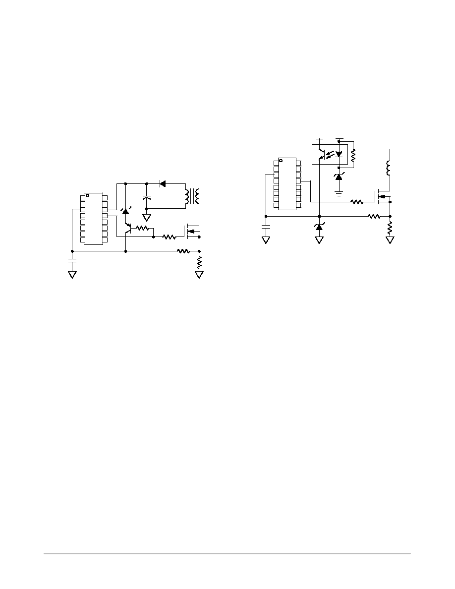
NCP1603
http://onsemi.com
28
In order to prevent wrongly triggering the latch
protection function, it is generaly recommended to put a
pF-order decoupling ceramic capacitor across the CS2 pin
to remove possible high-frequency noise there.
To set the V
CC
overvoltage protection, the circuit is
configured in Figure 74. A PNP bipolar transistor is added
to open the Zener diode Z
OVP
when Out2 is high in order
to stop any interference of the normal operation of current
sense. It is because the Zener diode easily pulls high the
CS2 pin voltage to 1.0 V and that interferes with the normal
operation of the current sense when the output is high. The
OVP threshold V
CC2(OVP)
is expressed in Equation 26.
VCC2(OVP)
+
VZOVP
)
3 V
(eq. 26)
Figure 74. V
CC
Latched OVP Application Circuit
CS2
NCP1603
V
CC2
R
CS2
Z
OVP
R
S2
(6) Latched Overvoltage Protection (OVP)
As long as an external protection on CS2 pin (Pin 3) does
not affect the normal regulation operation of current sense,
the protection can be implemented. An alternative is to
implement the output overvoltage protection by an
optocoupler in Figure 75. The leakage current of the added
circuit is up to the zener diode at the output voltage. When
there is no overvoltage, the leakage is small and it does not
affect the normal operation. A resistor paralleled to the
optocoupler is added to share the potential increasing
leakage current of the zener diode due to temperature
variation. The Zener diode at the output voltage is
recommended to be a 1 mA operating current at the
threshold voltage. Then, this current is coupled through the
optocoupler and inserts a similar order of current
(depending on the current-transfer-ratio CTR of the
optocoupler) into CS2 pin. The CS2 pin is capable of up to
100 mA and with an internal 9 V anti-parallel ESD diode
but it is recommended to put a 8.2 V Zener diode there to
further protect the pin.
Figure 75. Output Latched OVP Application Circuit
NCP1603
CS2
V
CC2
R
CS2
Z
OVP
R
S2
V
out
(7) Dual Thermal Shutdown (TSD)
The NCP1603 consists of two individual dies that
incorporates their individual thermal shutdown. The PFC
thermal circuitry disables the PFC gate drive Out1 and then
keeps the power switch off when its junction temperature
exceeds 170
∞C typically. The PFC gate drive Out1 is then
enabled once the temperature drops below typically 125
∞C
(i.e., 45
∞C hysteresis).
The PWM thermal circuitry disables the PWM gate drive
Out2 and then keeps the power switch off when its junction
temperature exceeds 165
∞C typically. The PWM gate drive
Out2 is then enabled once the temperature drops below
typically 140
∞C and the circuit is unplugged (to make V
CC2
drops below 4.0 V).

NCP1603
http://onsemi.com
29
PFC Toggling
The variation of the duty ratio in the PWM stage between
the PFC-on or PFC-off can be very large. When the
NCP1603 circuit is operating at some conditions between
PFC on and off boundary, the duty ratio variation can lead
to unwanted on/off toggling in the PFC stage. A current
feedforward resistor R
FF
is hence recommended to added
between V
aux
and CS2 pin (pins 1 and 3) in Figure 76 to
prevent the toggling. The value of R
FF
is much larger than
current sense feedback resistor R
S2
and plays very little
effect when V
aux
= 0 (or PFC is off). When V
aux
is available
(or PFC is on), the R
FF
creates a positive offset on the CS2
pin voltage and it allows the feedback voltage V
FB2
to only
shift slightly but provide a dramatic duty cycle reduction
in Figure 77. It slight movement of the feedback voltage
can reduce the change to reach the PFC stage on/off
threshold. Hence, the current feedforward resistor can help
to improve the toggling.
CS2
NCP1603
R
FF
R
S2
V
bulk
V
aux
Figure 76. Feedforward Resistor R
FF
Added
Figure 77. Timing Diagram of PWM Stage When R
FF
is Added
High duty when PFC is off.
Low duty when PFC is on.
Out 2
V
CS2
V
aux
V
FB2
3

NCP1603
http://onsemi.com
30
PACKAGE DIMENSIONS
SO-16
D SUFFIX
CASE 751B-05
ISSUE J
NOTES:
1. DIMENSIONING AND TOLERANCING PER
ANSI Y14.5M, 1982.
2. CONTROLLING DIMENSION: MILLIMETER.
3. DIMENSIONS A AND B DO NOT INCLUDE
MOLD PROTRUSION.
4. MAXIMUM MOLD PROTRUSION 0.15 (0.006)
PER SIDE.
5. DIMENSION D DOES NOT INCLUDE DAMBAR
PROTRUSION. ALLOWABLE DAMBAR
PROTRUSION SHALL BE 0.127 (0.005) TOTAL
IN EXCESS OF THE D DIMENSION AT
MAXIMUM MATERIAL CONDITION.
1
8
16
9
SEATING
PLANE
F
J
M
R
X 45
_
G
8 PL
P
-B-
-A-
M
0.25 (0.010)
B
S
-T-
D
K
C
16 PL
S
B
M
0.25 (0.010)
A
S
T
DIM
MIN
MAX
MIN
MAX
INCHES
MILLIMETERS
A
9.80
10.00
0.386
0.393
B
3.80
4.00
0.150
0.157
C
1.35
1.75
0.054
0.068
D
0.35
0.49
0.014
0.019
F
0.40
1.25
0.016
0.049
G
1.27 BSC
0.050 BSC
J
0.19
0.25
0.008
0.009
K
0.10
0.25
0.004
0.009
M
0
7
0
7
P
5.80
6.20
0.229
0.244
R
0.25
0.50
0.010
0.019
_
_
_
_
ON Semiconductor and are registered trademarks of Semiconductor Components Industries, LLC (SCILLC). SCILLC reserves the right to make changes without further notice
to any products herein. SCILLC makes no warranty, representation or guarantee regarding the suitability of its products for any particular purpose, nor does SCILLC assume any
liability arising out of the application or use of any product or circuit, and specifically disclaims any and all liability, including without limitation special, consequential or incidental
damages. "Typical" parameters which may be provided in SCILLC data sheets and/or specifications can and do vary in different applications and actual performance may vary over
time. All operating parameters, including "Typicals" must be validated for each customer application by customer's technical experts. SCILLC does not convey any license under
its patent rights nor the rights of others. SCILLC products are not designed, intended, or authorized for use as components in systems intended for surgical implant into the body,
or other applications intended to support or sustain life, or for any other application in which the failure of the SCILLC product could create a situation where personal injury or death
may occur. Should Buyer purchase or use SCILLC products for any such unintended or unauthorized application, Buyer shall indemnify and hold SCILLC and its officers, employees,
subsidiaries, affiliates, and distributors harmless against all claims, costs, damages, and expenses, and reasonable attorney fees arising out of, directly or indirectly, any claim of
personal injury or death associated with such unintended or unauthorized use, even if such claim alleges that SCILLC was negligent regarding the design or manufacture of the part.
SCILLC is an Equal Opportunity/Affirmative Action Employer. This literature is subject to all applicable copyright laws and is not for resale in any manner.
PUBLICATION ORDERING INFORMATION
N. American Technical Support: 800-282-9855 Toll Free
USA/Canada
Japan: ON Semiconductor, Japan Customer Focus Center
2-9-1 Kamimeguro, Meguro-ku, Tokyo, Japan 153-0051
Phone: 81-3-5773-3850
NCP1603/D
The products described herein (NCP1603), may be covered by one or more of the following U.S. patents: 6,271,735, 6,362,067, 6,385,060, 6,597,221,
6,970,365. There may be other patents pending.
LITERATURE FULFILLMENT:
Literature Distribution Center for ON Semiconductor
P.O. Box 61312, Phoenix, Arizona 85082-1312 USA
Phone: 480-829-7710 or 800-344-3860 Toll Free USA/Canada
Fax: 480-829-7709 or 800-344-3867 Toll Free USA/Canada
Email: orderlit@onsemi.com
ON Semiconductor Website: http://onsemi.com
Order Literature: http://www.onsemi.com/litorder
For additional information, please contact your
local Sales Representative.