 | –≠–ª–µ–∫—Ç—Ä–æ–Ω–Ω—ã–π –∫–æ–º–ø–æ–Ω–µ–Ω—Ç: NCP1653PG | –°–∫–∞—á–∞—Ç—å:  PDF PDF  ZIP ZIP |
©
Semiconductor Components Industries, LLC, 2005
December, 2005 - Rev. 4
1
Publication Order Number:
NCP1653/D
NCP1653, NCP1653A
Compact, Fixed-Frequency,
Continuous Conduction
Mode PFC Controller
The NCP1653 is a controller designed for Continuous Conduction
Mode (CCM) Power Factor Correction (PFC) boost circuits. It
operates in the follower boost or constant output voltage in 67 or 100
kHz fixed switching frequency. Follower boost offers the benefits of
reduction of output voltage and hence reduction in the size and cost
of the inductor and power switch. Housed in a DIP-8 or SO-8
package, the circuit minimizes the number of external components
and drastically simplifies the CCM PFC implementation. It also
integrates high safety protection features. The NCP1653 is a driver
for robust and compact PFC stages.
Features
∑
IEC1000-3-2 Compliant
∑
Continuous Conduction Mode
∑
Average Current-Mode or Peak Current-Mode Operation
∑
Constant Output Voltage or Follower Boost Operation
∑
Very Few External Components
∑
Fixed Switching Frequency: 67 kHz = NCP1653A,
Fixed Switching Frequency:
100 kHz = NCP1653
∑
Soft-Start Capability
∑
V
CC
Undervoltage Lockout with Hysteresis (8.7 / 13.25 V)
∑
Overvoltage Protection (107% of Nominal Output Level)
∑
Undervoltage Protection or Shutdown (8% of Nominal Output Level)
∑
Programmable Overcurrent Protection
∑
Programmable Overpower Limitation
∑
Thermal Shutdown with Hysteresis (120 / 150
_C)
∑
Pb-Free Packages are Available
Typical Applications
∑
TV & Monitors
∑
PC Desktop SMPS
∑
AC Adapters SMPS
∑
White Goods
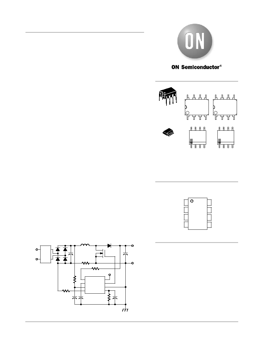
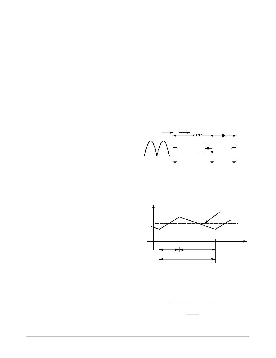
AC
Input
EMI
Filter
Output
In
Gnd
V
control
Drv
FB
V
CC
CS
V
M
15 V
NCP1653
Figure 1. Typical Application Circuit
PDIP-8
P SUFFIX
CASE 626
1
8
PIN CONNECTIONS
http://onsemi.com
MARKING DIAGRAMS
SO-8
D SUFFIX
CASE 751
1
FB
8 V
CC
2
V
control
3
In
4
CS
7 Drv
6 Gnd
5 V
M
(Top View)
A suffix = 67 kHz option
A
= Assembly Location
WL, L
= Wafer Lot
YY, Y
= Year
WW, W = Work Week
G
= Pb-Free Package
1
8
1
8
NCP1653
AWL
YYWW
http://onsemi.com
N1653
ALYW
G
1
8
1
8
NCP1653A
AWL
YYWW
1653A
ALYW
G
1
8
See detailed ordering and shipping information in the package
dimensions section on page 18 of this data sheet.
ORDERING INFORMATION
NCP1653, NCP1653A
http://onsemi.com
2
Figure 2. Functional Block Diagram
0 1
300 k
-
+
+
-
OR
1
8
4
5
2
3
7
6
9 V
0 1
1 0
x
+
9 V
AC
Input
EMI
Filter
C
filter
R
CS
C
bulk
off
on
R
FB
Output Voltage (V
out
)
L
I
FB
Current
Mirror
Overvoltage
Protection
(I
FB
> 107% I
ref
)
Thermal
Shutdown
(120 / 150
∞
C)
Current
Mirror
FB
ref
reg
V
I
I
96%
Regulation Block
ref
I
V
CC
Internal Bias
Reference Block
18 V
V
CC
V
CC
UVLO
FB / SD
9 V
Current
Mirror
V
CC
Output
Driver
S
R
Q
PFC
Modulation
C
ramp
Gnd
C
control
V
control
9 V
Overcurrent
Protection
(I
S
> 200
m
A)
I
L
I
L
V
in
I
in
V
M
I
M
13.25 V
/ 8.7 V
Turn on
R
vac
I
vac
C
vac
In
12 k
9 V
C
M
R
M
I
S
R
S
CS
Drv
67 or 100 kHz clock
V
ramp
V
ref
I
ch
Shutdown / UVP
(I
FB
< 8% I
ref
)
4% I
ref
Hysteresis
Overpower
Limitation
(I
S
I
vac
> 3 nA
2
)
I
control
=
V
control
R
1
V
M
=
R
M
I
S
I
vac
2 I
control
&
R
1
= constant
NCP1653, NCP1653A
http://onsemi.com
3
PIN FUNCTION DESCRIPTION
Pin
Symbol
Name
Function
1
FB / SD
Feedback /
Shutdown
This pin receives a feedback current I
FB
which is proportional to the PFC circuit output voltage.
The current is for output regulation, output overvoltage protection (OVP), and output
undervoltage protection (UVP).
When I
FB
goes above 107% I
ref
, OVP is activated and the Drive Output is disabled.
When I
FB
goes below 8% I
ref
, the device enters a low-consumption shutdown mode.
2
V
control
Control Voltage /
Soft-Start
The voltage of this pin V
control
directly controls the input impedance and hence the power
factor of the circuit. This pin is connected to an external capacitor C
control
to limit the V
control
bandwidth typically below 20 Hz to achieve near unity power factor.
The device provides no output when V
control
= 0 V. Hence, C
control
also works as a soft-start
capacitor.
3
In
Input Voltage
Sense
This pin sinks an input-voltage current I
vac
which is proportional to the RMS input voltage V
ac
.
The current I
vac
is for overpower limitation (OPL) and PFC duty cycle modulation. When the
product (I
S
I
vac
) goes above 3 nA
2
, OPL is activated and the Drive Output duty ratio is reduced
by pulling down V
control
indirectly to reduce the input power.
4
CS
Input Current
Sense
This pin sources a current I
S
which is proportional to the inductor current I
L
. The sense current
I
S
is for overcurrent protection (OCP), overpower limitation (OPL) and PFC duty cycle
modulation. When I
S
goes above 200
m
A, OCP is activated and the Drive Output is disabled.
5
V
M
Multiplier Voltage
This pin provides a voltage V
M
for the PFC duty cycle modulation. The input impedance of the
PFC circuit is proportional to the resistor R
M
externally connected to this pin. The device
operates in average current-mode if an external capacitor C
M
is connected to the pin.
Otherwise, it operates in peak current-mode.
6
GND
The IC Ground
-
7
Drv
Drive Output
This pin provides an output to an external MOSFET.
8
V
CC
Supply Voltage
This pin is the positive supply of the device. The operating range is between 8.75 V and 18 V
with UVLO start threshold 13.25 V.
MAXIMUM RATINGS
Rating
Symbol
Value
Unit
FB, V
control
, In, CS, V
M
Pins (Pins 1-5)
Maximum Voltage Range
Maximum Current
V
max
I
max
-0.3 to +9
100
V
mA
Drive Output (Pin 7)
Maximum Voltage Range
Maximum Current Range (Note 2)
V
max
I
max
-0.3 to +18
1.5
V
A
Power Supply Voltage (Pin 8)
Maximum Voltage Range
Maximum Current
V
max
I
max
-0.3 to +18
100
V
mA
Power Dissipation and Thermal Characteristics
P suffix, Plastic Package, Case 626
Maximum Power Dissipation @ T
A
= 70
∞
C
Thermal Resistance Junction-to-Air
D suffix, Plastic Package, Case 751
Maximum Power Dissipation @ T
A
= 70
∞
C
Thermal Resistance Junction-to-Air
P
D
R
q
JA
P
D
R
q
JA
800
100
450
178
mW
∞
C/W
mW
∞
C/W
Operating Junction Temperature Range
T
J
-40 to +125
∞
C
Storage Temperature Range
T
stg
-65 to +150
∞
C
1. Maximum Ratings are those values beyond which damage to the device may occur. Exposure to these conditions or conditions beyond those
indicated may adversely affect device reliability. Functional operation under absolute maximum-rated is not implied. Functional operation
should be restricted to the Recommended Operating Conditions.
A.
This device series contains ESD protection and exceeds the following tests:
Pins 1-8: Human Body Model 2000 V per MIL-STD-883, Method 3015.
Machine Model Method 190 V.
B.
This device contains Latchup protection and exceeds
±
100 mA per JEDEC Standard JESD78.
2. Guaranteed by design.
NCP1653, NCP1653A
http://onsemi.com
4
ELECTRICAL CHARACTERISTICS
(For typical values T
J
= 25
∞
C. For min/max values, T
J
= -40
∞
C to +125
∞
C, V
CC
= 15 V,
I
FB
= 100
m
A, I
vac
= 30
m
A, I
S
= 0
m
A, unless otherwise specified)
Characteristics
Pin
Symbol
Min
Typ
Max
Unit
OSCILLATOR
Switching Frequency
NCP1653
NCP1653A
7
f
SW
90
60.3
102
67
110
73.7
kHz
Maximum Duty Cycle (V
M
= 0 V) (Note 3)
7
D
max
94
-
-
%
GATE DRIVE
Gate Drive Resistor
Output High and Draw 100 mA out of Drv pin (I
source
= 100 mA)
Output Low and Insert 100 mA into Drv pin (I
sink
= 100 mA)
7
R
OH
R
OL
5.0
2.0
9.0
6.6
20
18
W
W
Gate Drive Rise Time from 1.5 V to 13.5 V (Drv = 2.2 nF to Gnd)
7
t
r
-
88
-
ns
Gate Drive Fall Time from 13.5 V to 1.5 V (Drv = 2.2 nF to Gnd)
7
t
f
-
61.5
-
ns
FEEDBACK / OVERVOLTAGE PROTECTION / UNDERVOLTAGE PROTECTION
Reference Current (V
M
= 3 V)
1
I
ref
192
204
208
m
A
Regulation Block Ratio
1
I
regL
/I
ref
95
96
98
%
Vcontrol Pin Internal Resistor
2
R
control
-
300
-
k
W
Maximum Control Voltage (I
FB
= 100
m
A)
2
V
control(max)
-
2.4
-
V
Maximum Control Current (I
control(max)
= I
ref
/ 2)
2
I
control(max)
-
100
-
m
A
Feedback Pin Voltage (I
FB
= 100
m
A)
Feedback Pin Voltage (I
FB
= 200
m
A)
1
V
FB1
1.0
1.3
1.5
1.8
1.9
2.2
V
V
Overvoltage Protection
OVP Ratio
Current Threshold
Propagation Delay
1
I
OVP
/I
ref
I
OVP
t
OVP
104
-
-
107
214
500
-
230
-
%
m
A
ns
Undervoltage Protection (V
M
= 3 V)
UVP Activate Threshold Ratio
UVP Deactivate Threshold Ratio
UVP Lockout Hysteresis
Propagation Delay
1
I
UVP(on)
/I
ref
I
UVP(off)
/I
ref
I
UVP(H)
t
UVP
4.0
7.0
4.0
-
8.0
12
8.0
500
15
20
-
-
%
%
m
A
ns
CURRENT SENSE
Current Sense Pin Offset Voltage (I
S
= 100
m
A)
4
V
S
0
10
30
mV
Overcurrent Protection Threshold (V
M
= 1 V)
4
I
S(OCP)
185
200
215
m
A
OVERPOWER LIMITATION
Input Voltage Sense Pin Internal Resistor
4
R
vac(int)
-
12
-
k
W
Over Power Limitation Threshold
3-4
I
S
◊
I
vac
-
3.0
-
nA
2
Sense Current Threshold (I
vac
= 30
m
A, V
M
= 3 V)
Sense Current Threshold (I
vac
= 100
m
A, V
M
= 3 V)
4
I
S(OPL1)
I
S(OPL2)
80
24
100
32
140
48
m
A
m
A
CURRENT MODULATION
PWM Comparator Reference Voltage
5
V
ref
2.25
2.62
2.75
V
Multiplier Current (V
control
= V
control(max)
, I
vac
= 30
m
A, I
S
= 25
m
A)
Multiplier Current (V
control
= V
control(max)
, I
vac
= 30
m
A, I
S
= 75
m
A)
Multiplier Current (V
control
= V
control(max)
/ 10, I
vac
= 30
m
A, I
S
= 25
m
A)
Multiplier Current (V
control
= V
control(max)
/ 10, I
vac
= 30
m
A, I
S
= 75
m
A)
5
I
M1
I
M2
I
M3
I
M4
1.0
3.2
10
30
2.85
9.5
35
103.5
5.8
18
58
180
m
A
m
A
m
A
m
A
THERMAL SHUTDOWN
Thermal Shutdown Threshold (Note 3)
-
T
SD
150
-
-
∞
C
Thermal Shutdown Hysteresis
-
-
-
30
-
∞
C
3. Guaranteed by design.
NCP1653, NCP1653A
http://onsemi.com
5
ELECTRICAL CHARACTERISTICS
(For typical values T
J
= 25
∞
C. For min/max values, T
J
= -40
∞
C to +125
∞
C, V
CC
= 15 V,
I
FB
= 100
m
A, I
vac
= 30
m
A, I
S
= 0
m
A, unless otherwise specified)
Characteristics
Unit
Max
Typ
Min
Symbol
Pin
SUPPLY SECTION
Supply Voltage
UVLO Startup Threshold
Minimum Operating Voltage after Startup
UVLO Hysteresis
8
V
CC(on)
V
CC(off)
V
CC(H)
12.25
8.0
4.0
13.25
8.7
4.55
14.5
9.5
-
V
V
V
Supply Current:
Startup (V
CC
= V
CC(on)
- 0.2 V)
Startup (V
CC
< 4.0 V, I
FB
= 200
m
A)
Startup (4.0 V < V
CC
< V
CC(on)
- 0.2 V, I
FB
= 200
m
A)
Startup (V
CC
< V
CC(on)
- 0.2 V, I
FB
= 0
m
A) (Note 4)
Operating (V
CC
= 15 V, Drv = open, V
M
= 3 V)
Operating (V
CC
= 15 V, Drv = 1 nF to Gnd, V
M
= 1 V)
Shutdown (V
CC
= 15 V and I
FB
= 0 A)
8
I
stup
I
stup1
I
stup2
I
stup3
I
CC1
I
CC2
I
stdn
-
-
-
-
-
-
-
18
0.95
21
21
3.7
4.7
33
50
1.5
50
50
5.0
6.0
50
m
A
mA
m
A
m
A
mA
mA
m
A
4. Please refer to the "Biasing the Controller" Section in the Functional Description.
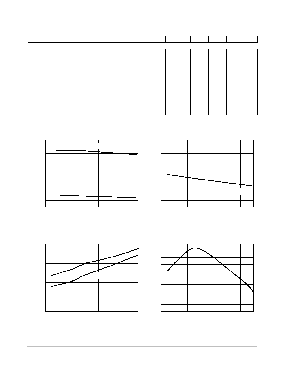
TYPICAL CHARACTERISTICS
f
SW
, SWITCHING FREQUENCY (kHz)
Figure 3. Switching Frequency vs. Temperature
T
J
, JUNCTION TEMPERATURE (
∞
C)
60
65
70
75
80
85
90
-50
0
25
50
75
100
125
Figure 4. Maximum Duty Cycle vs. Temperature
Figure 5. Gate Drive Resistance vs. Temperature
Figure 6. Reference Current vs. Temperature
-25
95
100
105
110
D
ma
x
, MAXIMUM DUTY CYCLE (%)
T
J
, JUNCTION TEMPERATURE (
∞
C)
90
91
92
93
94
95
96
-50
0
25
50
75
100
125
-25
97
V
M
= 0 V
R
OH
& R
OL
, GA
TE DRIVE RESIST
ANCE (
W
)
T
J
, JUNCTION TEMPERATURE (
∞
C)
0
2
4
6
-50
0
25
50
75
100
125
-25
8
10
I
ref
, REFERENCE CURRENT (
m
A)
T
J
, JUNCTION TEMPERATURE (
∞
C)
195
196
197
198
199
200
201
-50
0
25
50
75
100
125
-25
202
R
OH
203
205
98
99
100
12
14
R
OL
204
NCP1653
NCP1653A
NCP1653, NCP1653A
http://onsemi.com
6
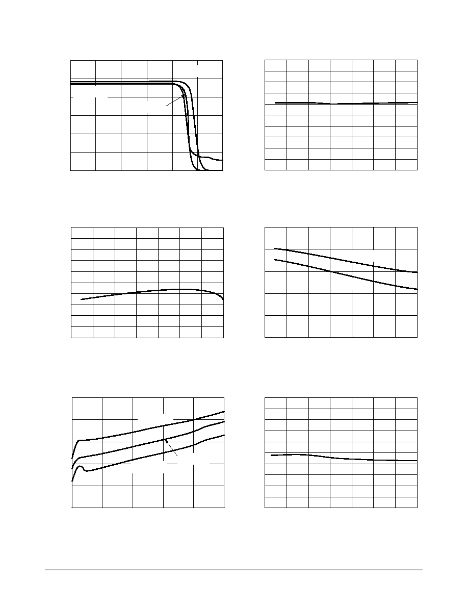
TYPICAL CHARACTERISTICS
MAXIMUM
CONTROL VOL
T
AGE (V)
T
J
, JUNCTION TEMPERATURE (
∞
C)
2.0
2.2
2.4
2.6
2.8
3.0
-50
0
25
50
75
100
125
-25
FEEDBACK PIN VOL
T
AGE (V)
I
FB
, FEEDBACK PIN CURRENT (
m
A)
1
1.5
2
2.5
50
100
150
200
250
0
OVER
VOL
T
AGE PROTECTION RA
TIO (%)
T
J
, JUNCTION TEMPERATURE (
∞
C)
100
102
104
106
108
110
112
-50
0
25
50
75
100
125
-25
114
116
120
T
J
= 25
∞
C
0
0.5
118
T
J
= -40
∞
C
T
J
= 125
∞
C
V
co
n
t
r
o
l
, CONTROL VOL
T
AGE (V)
Figure 7. Regulation Block
Figure 8. Regulation Block Ratio vs.
Temperature
0
0.5
1
1.5
2
3
100
120
140
160
180
200
220
I
FB
, FEEDBACK CURRENT (
m
A)
T
J
= 25
∞
C
2.5
T
J
= 125
∞
C
T
J
= -40
∞
C
Figure 9. Maximum Control Voltage vs.
Temperature
Figure 10. Feedback Pin Voltage vs.
Temperature
Figure 11. Feedback Pin Voltage vs. Feedback
Current
Figure 12. Overvoltage Protection Ratio
vs. Temperature
REGULA
TION
BLOCK RA
TIO (%)
T
J
, JUNCTION TEMPERATURE (
∞
C)
90
91
92
93
94
95
96
-50
0
25
50
75
100
125
-25
97
98
99
100
FEEDBACK PIN VOL
T
AGE (V)
T
J
, JUNCTION TEMPERATURE (
∞
C)
1
1.5
2
2.5
-25
0
25
100
125
-50
0
0.5
I
FB
= 200
m
A
2.1
2.3
2.5
2.7
2.9
50
75
I
FB
= 100
m
A
NCP1653, NCP1653A
http://onsemi.com
7
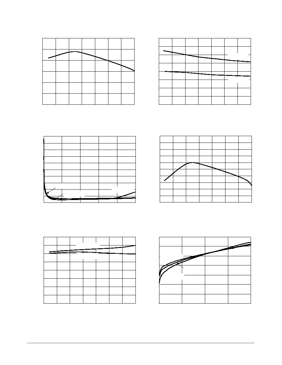
TYPICAL CHARACTERISTICS
CURRENT
SENSE PIN VOL
T
AGE (mV)
I
S
, SENSE CURRENT (
m
A)
0
20
40
60
80
100
0
100
150
200
250
50
T
J
= -40
∞
C
OVERPOWER LIMIT
A
TION THRESHOLD (nA
2
)
T
J
, JUNCTION TEMPERATURE (
∞
C)
-50
0
25
50
75
100
125
-25
V
va
c
, IN PIN VOL
T
AGE (V)
I
vac
, INPUT-VOLTAGE CURRENT (
m
A)
0
1
2
3
4
5
6
0
50
150
100
200
7
0
0.5
1
1.5
2
2.5
3
3.5
4
T
J
= 25
∞
C
T
J
= 125
∞
C
Figure 13. Overvoltage Protection Threshold
vs. Temperature
Figure 14. Undervoltage Protection
Thresholds vs. Temperature
OVER
VOL
T
AGE PROTECTION THRESHOLD (
m
A)
T
J
, JUNCTION TEMPERATURE (
∞
C)
220
225
230
-50
0
25
50
75
100
125
-25
UNDER
VOL
T
AGE PROTECTION
THRESHOLD RA
TIO (%)
T
J
, JUNCTION TEMPERATURE (
∞
C)
0
2
4
6
8
10
12
-50
0
25
50
75
100
125
-25
14
16
200
205
210
215
Figure 15. Current Sense Pin Voltage vs.
Sense Current
Figure 16. Overcurrent Protection Threshold
vs. Temperature
Figure 17. Overpower Limitation Threshold
vs. Temperature
Figure 18. In Pin Voltage vs.
Input-Voltage Current
OVERCURRENT PROTECTION
THRESHOLD (
m
A)
T
J
, JUNCTION TEMPERATURE (
∞
C)
198
200
202
204
206
208
210
-50
0
25
50
75
100
125
-25
190
192
194
196
I
vac
= 100
m
A
I
vac
= 30
m
A
T
J
= -40
∞
C
T
J
= 25
∞
C
T
J
= 125
∞
C
I
UVP(off)
/I
ref
I
UVP(on)
/I
ref
10
30
50
70
90
NCP1653, NCP1653A
http://onsemi.com
8
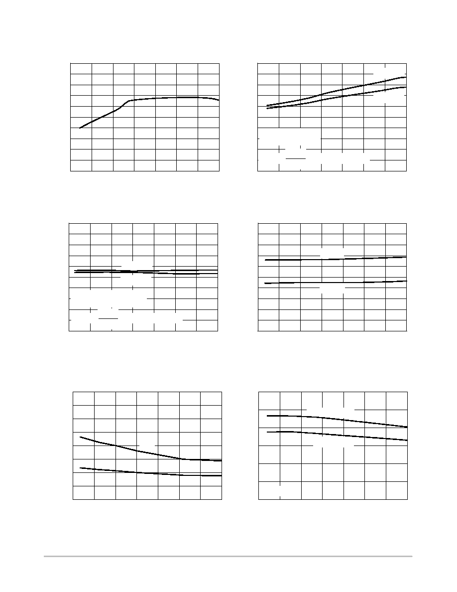
TYPICAL CHARACTERISTICS
1
0
%
OF MAXIMUM CONTROL CURRENT (
m
A)
T
J
, JUNCTION TEMPERATURE (
∞
C)
0
4
8
12
-50
0
25
50
75
100
125
-25
SUPPL
Y
V
O
L
T
AGE UNDER
VOL
T
AGE
LOCKOUT THRESHOLDS (V)
T
J
, JUNCTION TEMPERATURE (
∞
C)
0
2
4
6
8
10
12
-50
0
25
50
75
100
125
-25
V
CC
= 15 V
I
stdn
V
CC(on)
V
CC(off)
I
stup
SUPPL
Y CURRENT
IN ST
AR
TUP AND
SHUTDOWN MODE (
m
A)
T
J
, JUNCTION TEMPERATURE (
∞
C)
0
10
20
30
40
50
70
-50
0
25
50
75
100
125
-25
OPERA
TING
SUPPL
Y CURRENT (mA)
T
J
, JUNCTION TEMPERATURE (
∞
C)
0
1
2
3
4
5
-50
0
25
50
75
100
125
-25
2
6
10
60
I
CC2
, 1 nF Load
I
CC1
, No Load
Figure 19. PWM Comparator Reference
Voltage vs. Temperature
Figure 20. Maximum Control Current vs.
Temperature
P
W
M
C
O
M
P
ARA
T
OR REF
. VOL
T
AGE (V)
T
J
, JUNCTION TEMPERATURE (
∞
C)
2
2.1
2.2
2.3
2.4
2.5
2.7
-50
0
25
50
75
100
125
-25
MAXIMUM CONTROL CURRENT (
m
A)
T
J
, JUNCTION TEMPERATURE (
∞
C)
0
20
40
60
80
100
140
-50
0
25
50
75
100
125
-25
2.6
120
160
180
Figure 21. 10% of Maximum Control Current
vs. Temperature
Figure 22. Supply Voltage Undervoltage
Lockout Thresholds vs. Temperature
Figure 23. Supply Current in Startup and
Shutdown Mode vs. Temperature
Figure 24. Operating Supply Current vs.
Temperature
2.8
3
2.9
I
vac
= 30
m
A
V
control
= V
control(max)
I
S
= 25
m
A
I
S
= 75
m
A
I
vac
= 30
m
A
V
control
= 10 % V
control(max)
I
S
= 25
m
A
I
S
= 75
m
A
14
16
80
6
I
control
=
derived from the (eq.8)
I
S
I
vac
2I
M
I
control
=
derived from the (eq.8)
I
S
I
vac
2I
M
200
16
20
14
18
18
20
NCP1653, NCP1653A
http://onsemi.com
9
FUNCTIONAL DESCRIPTION
Introduction
The NCP1653 is a Power Factor Correction (PFC) boost
controller designed to operate in fixed-frequency
Continuous Conduction Mode (CCM). It can operate in
either peak current-mode or average current-mode.
Fixed-frequency operation eases the compliance with
EMI standards and the limitation of the possible radiated
noise that may pollute surrounding systems. The CCM
operation reduces the application di/dt and the resulting
interference. The NCP1653 is designed in a compact 8-pin
package which offers the minimum number of external
components. It simplifies the design and reduces the cost.
The output stage of the NCP1653 incorporates
±1.5 A
current capability for direct driving of the MOSFET in
high-power applications.
The NCP1653 is implemented in constant output voltage
or follower boost modes. The follower boost mode permits
one to significantly reduce the size of the PFC circuit
inductor and power MOSFET. With this technique, the
output voltage is not set at a constant level but depends on
the RMS input voltage or load demand. It allows lower
output voltage and hence the inductor and power MOSFET
size or cost are reduced.
Hence, NCP1653 is an ideal candidate in high-power
applications where cost-effectiveness, reliability and high
power factor are the key parameters. The NCP1653
incorporates all the necessary features to build a compact
and rugged PFC stage.
The NCP1653 provides the following protection features:
1. Overvoltage Protection (OVP) is activated and
the Drive Output (Pin 7) goes low when the
output voltage exceeds 107% of the nominal
regulation level which is a user-defined value.
The circuit automatically resumes operation when
the output voltage becomes lower than the 107%.
2. Undervoltage Protection (UVP) is activated and
the device is shut down when the output voltage
goes below 8% of the nominal regulation level.
The circuit automatically starts operation when
the output voltage goes above 12% of the
nominal regulation level. This feature also
provides output open-loop protection, and an
external shutdown feature.
3. Overpower Limitation (OPL) is activated and the
Drive Output (Pin 7) duty ratio is reduced by
pulling down an internal signal when a computed
input power exceeds a permissible level. OPL is
automatically deactivated when this computed input
power becomes lower than the permissible level.
4. Overcurrent Protection (OCP) is activated and
the Drive Output (Pin 7) goes low when the
inductor current exceeds a user-defined value.
The operation resumes when the inductor current
becomes lower than this value.
5. Thermal Shutdown (TSD) is activated and the
Drive Output (Pin 7) is disabled when the
junction temperature exceeds 150
_C. The
operation resumes when the junction temperature
falls down by typical 30
_C.
CCM PFC Boost
A CCM PFC boost converter is shown in Figure 25. The
input voltage is a rectified 50 or 60 Hz sinusoidal signal.
The MOSFET is switching at a high frequency (typically
102 kHz in the NCP1653) so that the inductor current I
L
basically consists of high and low-frequency components.
Filter capacitor C
filter
is an essential and very small value
capacitor in order to eliminate the high-frequency
component of the inductor current I
L
. This filter capacitor
cannot be too bulky because it can pollute the power factor
by distorting the rectified sinusoidal input voltage.
Figure 25. CCM PFC Boost Converter
V
in
I
in
I
L
L
V
out
C
bulk
C
filter
PFC Methodology
The NCP1653 uses a proprietary PFC methodology
particularly designed for CCM operation. The PFC
methodology is described in this section.
Figure 26. Inductor Current in CCM
I
in
t 2
t 1
time
T
I L
As shown in Figure 26, the inductor current I
L
in a
switching period T includes a charging phase for duration
t
1
and a discharging phase for duration t
2
. The voltage
conversion ratio is obtained in (eq.1).
Vout
Vin
+
t1
)
t2
t2
+
T
T
*
t1
Vin
+
T
*
t1
T
Vout
(eq.1)
NCP1653, NCP1653A
http://onsemi.com
10
The input filter capacitor C
filter
and the front-ended EMI
filter absorbs the high-frequency component of inductor
current I
L
. It makes the input current I
in
a low-frequency
signal only of the inductor current.
Iin
+
IL-50
(eq.2)
The suffix 50 means it is with a 50 or 60 Hz bandwidth
of the original I
L
.
From (eq.1) and (eq.2), the input impedance Z
in
is
formulated.
Zin
+
Vin
Iin
+
T
*
t1
T
Vout
IL-50
(eq.3)
Power factor is corrected when the input impedance Z
in
in (eq.3) is constant or slowly varying in the 50 or 60 Hz
bandwidth.
Figure 27. PFC Duty Modulation and Timing Diagram
R
S
Q
0 1
clock
PFC Modulation
Output
Clock
Latch Set
Latch Reset
Inductor
Current
without
filtering
-
+
+
V
ref
V
ref
V
ramp
V
ramp
V
M
V
M
V
M
I
ch
C
ramp
The PFC duty modulation and timing diagram is shown
in Figure 27. The MOSFET on time t
1
is generated by the
intersection of reference voltage V
ref
and ramp voltage
V
ramp
. A relationship in (eq.4) is obtained.
Vramp
+
VM
)
Icht1
Cramp
+
Vref
(eq.4)
The charging current I
ch
is specially designed as in
(eq.5). The multiplier voltage V
M
is therefore expressed in
terms of t
1
in (eq.6).
Ich
+
Cramp Vref
T
(eq.5)
(eq.6)
VM
+
Vref
*
t1
Cramp
CrampVref
T
+
Vref
T
*
t1
T
From (eq.3) and (eq.6), the input impedance Z
in
is
re-formulated in (eq.7).
(eq.7)
Zin
+
VM
Vref
Vout
IL-50
Because V
ref
and V
out
are roughly constant versus time,
the multiplier voltage V
M
is designed to be proportional to
the I
L-50
in order to have a constant Z
in
for PFC purpose.
It is illustrated in Figure 28.
Figure 28. Multiplier Voltage Timing Diagram
V in
time
time
V M
time
I in
I L
It can be seen in the timing diagram in Figure 27 that V
M
originally consists of a switching frequency ripple coming
from the inductor current I
L
. The duty ratio can be
inaccurately generated due to this ripple. This modulation
is the so-called "peak current-mode". Hence, an external
capacitor C
M
connected to the multiplier voltage V
M
pin
(Pin 5) is essential to bypass the high-frequency
component of V
M
. The modulation becomes the so-called
"average current-mode" with a better accuracy for PFC.
Figure 29. External Connection on the Multiplier
Voltage Pin
5
R
M
I
vac
I
S
2I
control
V
M
=
PFC Duty
Modulation
I
M
V
M
R
M
C
M
The multiplier voltage V
M
is generated according to
(eq.8).
VM
+
RM Ivac IS
2 Icontrol
(eq.8)
Input-voltage current I
vac
is proportional to the RMS
input voltage V
ac
as described in (eq.9). The suffix ac
NCP1653, NCP1653A
http://onsemi.com
11
stands for the RMS. I
vac
is a constant in the 50 or 60 Hz
bandwidth. Multiplier resistor R
M
is the external resistor
connected to the multiplier voltage V
M
pin (Pin 5). It is also
constant. R
M
directly limits the maximum input power
capability and hence its value affects the NCP1653 to
operate in either "follower boost mode" or " constant
output voltage mode".
Ivac
+
2 Vac
*
4 V
(Rvac
)
12 k
W
)
[
Vac
R vac
(eq.9)
Sense current I
S
is proportional to the inductor current I
L
as described in (eq.10). I
L
consists of the high-frequency
component (which depends on di/dt or inductor L) and
low-frequency component (which is I
L-50
).
IS
+
RCS
RS
IL
(eq.10)
Control current I
control
is a roughly constant current that
comes from the PFC output voltage V
out
that is a slowly
varying signal. The bandwidth of I
control
can be
additionally limited by inserting an external capacitor
C
control
to the control voltage V
control
pin (Pin 2) in
Figure 30. It is recommended to limit f
control
, that is the
bandwidth of V
control
(or I
control
), below 20 Hz typically to
achieve power factor correction purpose. Typical value of
C
control
is between 0.1
mF and 0.33 mF.
Figure 30. V
control
Low-Pass Filtering
FB
ref
ref
reg
300 k
Ccontrol
V
I
I
96% I
Regulation Block
2
Vcontrol
I =
control
Vcontrol
R 1
(eq.11)
Ccontrol
u
1
2
p
300 k
W
fcontrol
From (eq.7)-(eq.10), the input impedance Z
in
is
re-formulated in (eq.12).
Zin
+
RM RCS Vac Vout IL
2 RS R vac Icontrol Vref IL-50
Zin
+
RM RCS Vac Vout
2 RS R vac Icontrol Vref
whenIL
+
IL-50
(eq.12)
The multiplier capacitor C
M
is the one to filter the
high-frequency component of the multiplier voltage V
M
.
The high-frequency component is basically coming from
the inductor current I
L
. On the other hand, the filter
capacitor C
filter
similarly removes the high-frequency
component of inductor current I
L
. If the capacitors C
M
and
C
filter
match with each other in terms of filtering capability,
I
L
becomes I
L-50
. Input impedance Z
in
is roughly constant
over the bandwidth of 50 or 60 Hz and power factor is
corrected.
Practically, the differential-mode inductance in the
front-ended EMI filter improves the filtering performance
of capacitor C
filter
. Therefore, the multiplier capacitor C
M
is generally with a larger value comparing to the filter
capacitor C
filter
.
Input and output power (P
in
and P
out
) are derived in
(eq.13) when the circuit efficiency
is obtained or
assumed. The variable V
ac
stands for the RMS input
voltage.
Pin
+
Vac2
Zin
+
2 RS R vac Icontrol Vref Vac
RM RCS Vout
(eq.13a)
T
Icontrol Vac
Vout
Pout
+ h
Pin
+ h
2 RS R vac Icontrol Vref Vac
RM RCS Vout
(eq.13b)
T
Icontrol Vac
Vout
Follower Boost
The NCP1653 operates in follower boost mode when
I
control
is constant. If I
control
is constant based on (eq.13), for
a constant load or power demand the output voltage V
out
of
the converter is proportional to the RMS input voltage V
ac
. It
means the output voltage V
out
becomes lower when the RMS
input voltage V
ac
becomes lower. On the other hand, the
output voltage V
out
becomes lower when the load or power
demand becomes higher. It is illustrated in Figure 31.
Figure 31. Follower Boost Characteristics
Vin
V (Follower boost)
out
time
time
V (Traditional boost)
out
Pout
Follower Boost Benefits
The follower boost circuit offers an opportunity to reduce
the output voltage V
out
whenever the RMS input voltage
V
ac
is lower or the power demand P
out
is higher. Because
of the step-up characteristics of boost converter, the output
voltage V
out
will always be higher than the input voltage
NCP1653, NCP1653A
http://onsemi.com
12
V
in
even though V
out
is reduced in follower boost operation.
As a result, the on time t
1
is reduced. Reduction of on time
makes the loss of the inductor and power MOSFET smaller.
Hence, it allows cheaper cost in the inductor and power
MOSFET or allows the circuit components to operate at a
lower stress condition in most of the time.
Output Feedback
The output voltage V
out
of the PFC circuit is sensed as a
feedback current I
FB
flowing into the FB pin (Pin 1) of the
device. Since the FB pin voltage V
FB1
is much smaller than
V
out
, it is usually neglected.
(eq.14)
IFB
+
Vout
*
VFB1
RFB
[
Vout
RFB
where R
FB
is the feedback resistor across the FB pin
(Pin 1) and the output voltage referring to Figure 2.
Then, the feedback current I
FB
represents the output
voltage V
out
and will be used in the output voltage
regulation, undervoltage protection (UVP), and
overvoltage protection (OVP).
Output Voltage Regulation
Feedback current I
FB
which represents the output voltage
V
out
is processed in a function with a reference current
(I
ref
= 200
mA typical) as shown in regulation block
function in Figure 32. The output of the voltage regulation
block, low-pass filter on V
control
pin and the I
control
=
V
control
/ R
1
block is in Figure 30 is control current I
control
.
And the input is feedback current I
FB
. It means that I
control
is the output of I
FB
and it can be described as in Figure 32.
There are three linear regions including: (1) I
FB
< 96%
◊
I
ref
, (2) 96%
◊ I
ref
<I
FB
< I
ref
, and (3) I
FB
> I
ref
. They are
discussed separately as follows:
Figure 32. Regulation Block
I
control
I
ref
I
ref
96%
I
FB
I
control(max)
Region (1): I
FB
< 96%
◊
I
ref
When I
FB
is less than 96% of I
ref
(i.e., V
out
< 96% R
FB
◊ I
ref
), the NCP1653 operates in follower boost mode. The
regulation block output V
reg
is at its maximum value.
I
control
becomes its maximum value (i.e., I
control
=
I
control(max)
= I
ref
/2 = 100
mA) which is a constant. (eq.13)
becomes (eq.15).
Vout
+ h
2 RS R vac Icontrol(max) Vref Vac
RM RCS Pout
(eq.15)
T
Vac
Pout
The output voltage V
out
is regulated at a particular level
with a particular value of RMS input voltage V
ac
and output
power P
out
. However, this output level is not constant and
depending on different values of V
ac
and P
out
. The follower
boost operating area is illustrated in Figure 33.
Figure 33. Follower Boost Region
V
V
V
Vout
ac(max)
ac(min)
ac
Pout(min)
Pout(max)
1
2
V in
96% I
ref
R
FB
1. P
out
increases, V
out
decreases
2. V
ac
decreases, V
out
decreases
Region (2): 96%
◊
I
ref
< I
FB
< I
ref
When I
FB
is between 96% and 100% of I
ref
(i.e., 96% R
FB
◊ I
ref
< V
out
< R
FB
◊ I
ref
), the NCP1653 operates in constant
output voltage mode which is similar to the follower boost
mode characteristic but with narrow output voltage range.
The regulation block output V
reg
decreases linearly with
I
FB
in the range from 96% of I
ref
to I
ref
. It gives a linear
function of I
control
in (eq.16).
(eq.16)
Icontrol
+
Icontrol(max)
0.04
1
*
Vout
RFB Iref
Resolving (eq.16) and (eq.13),
Vout
+
Vac
RM RCS
2 RS R vac Vref
0.04
Icontrol(max)
Pout
h
)
Vac
RFB Iref
(eq.17)
According to (eq.17), output voltage V
out
becomes R
FB
◊ I
ref
when power is low (P
out
0). It is the maximum value
of V
out
in this operating region. Hence, it can be concluded
that output voltage increases when power decreases. It is
similar to the follower boost characteristic in (eq.15). On
the other hand in (eq.17), output voltage V
out
becomes R
FB
◊ I
ref
when RMS input voltage V
ac
is very high. It is the
maximum value of V
out
in this operating region. Hence, it
can also be concluded that output voltage increases when
RMS input voltage increases. It is similar to another
follower boost characteristic in (eq.15). This characteristic
is illustrated in Figure 34.
Figure 34. Constant Output Voltage Region
V
V
V
Vout
ac(max)
ac(min)
ac
Pout(min)
Pout(max)
1
2
96% I
ref
R
FB
1. P
out
increases, V
out
decreases
2. V
ac
decreases, V
out
decreases
I
ref
R
FB
Region (3): I
FB
> I
ref
When I
FB
is greater than I
ref
(i.e., V
out
> R
FB
◊ I
ref
), the
NCP1653 provides no output or zero duty ratio. The
regulation block output V
reg
becomes 0 V. I
control
also

NCP1653, NCP1653A
http://onsemi.com
13
becomes zero. The multiplier voltage V
M
in (eq.8)
becomes its maximum value and generates zero on time t
1
.
Then, V
out
decreases and the minimum can be V
out
= V
in
in
a boost converter. Going down to V
in
, V
out
automatically
enters the previous two regions (i.e., follower boost region
or constant output voltage region) and hence output voltage
V
out
cannot reach input voltage V
in
as long as the NCP1653
provides a duty ratio for the operation of the boost
converter.
In conclusion, the NCP1653 circuit operates in one of the
following conditions:
Constant output voltage mode: The output voltage is
regulated around the range between 96% and 100% of R
FB
◊ I
ref
. The output voltage is described in (eq.16). Its
behavior is similar to a follower boost.
Follower boost mode: The output voltage is regulated
under 96% of R
FB
◊ I
ref
and I
control
= I
control(max)
= I
ref
/2 =
100
mA. The output voltage is described in (eq.15).
Overvoltage Protection (OVP)
When the feedback current I
FB
is higher than 107% of the
reference current I
ref
(i.e., V
out
> 107% R
FB
◊ I
ref
), the
Drive Output (Pin 7) of the device goes low for protection.
The circuit automatically resumes operation when the
feedback current becomes lower than 107% of the
reference current I
ref
.
The maximum OVP threshold is limited to 230
mA which
corresponds to 230
mA ◊ 1.92 MW + 2.5 V = 444.1 V when
R
FB
= 1.92 M
W (680 kW + 680 kW + 560 kW) and
V
FB1
= 2.5 V (for the worst case referring to Figure 11).
Hence, it is generally recommended to use 450 V rating
output capacitor to allow some design margin.
Undervoltage Protection (UVP)
Figure 35. Undervoltage Protection
I
8% I
12% I
FB
Shutdown
Operating
ref
ref
I
CC
I
CC2
I
stdn
When the feedback current I
FB
is less than 8% of the
reference current I
ref
(i.e., the output voltage V
out
is less
than 8% of its nominal value), the device is shut down and
consumes less than 50
mA. The device automatically starts
operation when the output voltage goes above 12% of the
nominal regulation level. In normal situation of boost
converter configuration, the output voltage V
out
is always
greater than the input voltage V
in
and the feedback current
I
FB
is always greater than 8% and 12% of the nominal level
to enable the NCP1653 to operate. Hence, UVP happens
when the output voltage is abnormally undervoltage, the
FB pin (Pin 1) is opened, or the FB pin (Pin 1) is manually
pulled low.
Soft-Start
The device provides no output (or no duty ratio) when the
V
control
(Pin 2) voltage is zero (i.e., V
control
= 0 V). An
external capacitor C
control
connected to the V
control
pin
provides a gradually increment of the V
control
voltage (or
the duty ratio) in the startup and hence provides a soft-start
feature.
Current Sense
The device senses the inductor current I
L
by the current
sense scheme in Figure 36. The device maintains the
voltage at the CS pin (Pin 4) to be zero voltage (i.e.,
V
S
0 V) so that (eq.10) can be formulated.
Figure 36. Current Sensing
CS
NCP1653
Gnd
+
-
R
CS
R
S
I
L
I
S
I
L
V
S
This scheme has the advantage of the minimum number
of components for current sensing and the inrush current
limitation by the resistor R
CS
. Hence, the sense current I
S
represents the inductor current I
L
and will be used in the
PFC duty modulation to generate the multiplier voltage
V
M
, Overpower Limitation (OPL), and overcurrent
protection.
Overcurrent Protection (OCP)
Overcurrent protection is reached when I
S
is larger than
I
S(OCP)
(200
mA typical). The offset voltage of the CS pin
is typical 10 mV and it is neglected in the calculation.
Hence, the maximum OCP inductor current threshold
I
L(OCP)
is obtained in (eq.15).
(eq.18)
IL(OCP)
+
RSIS(OCP)
RCS
+
RS
RCS
200
m
A
When overcurrent protection threshold is reached, the
Drive Output (Pin 7) of the device goes low. The device
automatically resumes operation when the inductor current
goes below the threshold.
Input Voltage Sense
The device senses the RMS input voltage V
ac
by the
sensing scheme in Figure 37. The internal current mirror is
with a typical 4 V offset voltage at its input so that the
current I
vac
can be derived in (eq.9). An external capacitor
NCP1653, NCP1653A
http://onsemi.com
14
C
vac
is to maintain the In pin (Pin 3) voltage in the
calculation to always be the peak of the sinusoidal voltage
due to very little current consumption (i.e., V
in
=
2 V
ac
and
I
vac
0). This I
vac
current represents the RMS input voltage
V
ac
and will be used in overpower limitation (OPL) and the
PFC duty modulation.
Figure 37. Input Voltage Sensing
In
Current
Mirror
3
12 k
Cvac
Rvac
Ivac
4 V
V in
9 V
There is an internal 9 V ESD Zener Diode on the pin.
Hence, the value of R
vac
is recommended to be at least
938 k
for possibly up to 400 V instantaneous input voltage.
Rvac
400 V
*
9 V
u
12 k
W
9 V
*
4 V
(eq.19)
Rvac
u
938 k
W
Overpower Limitation (OPL)
Sense current I
S
represents the inductor current I
L
and
hence represents the input current approximately.
Input-voltage current I
vac
represents the RMS input
voltage V
ac
and hence represents the input voltage. Their
product (I
S
◊ I
vac
) represents an approximated input power
(I
L
◊ V
ac
).
Figure 38. Overpower Limitation Reduces V
control
FB
ref
ref
reg
300 k
Vcontrol
V
I
I
96% I
Limitation
Overpower
Regulation Block
2
0 1
When the product (I
S
◊ I
vac
) is greater than a permissible
level 3 nA
2
, the output V
reg
of the regulation block is pulled
to 0 V. It makes V
control
to be 0 V indirectly and V
M
is
pulled to be its maximum. It generates the minimum duty
ratio or no duty ratio eventually so that the input power is
limited. The OPL is automatically deactivated when the
product (I
S
◊ I
vac
) becomes lower than the 3 nA
2
level. This
3 nA
2
level corresponds to the approximated input power
(I
L
◊ V
ac
) to be smaller than the particular expression in
(eq.20).
IS Ivac
t
3 nA2
IL
@
RCS
RS
Vac
@
2
Rvac
)
12 k
W t
3 nA2
IL
@
Vac
t
RS
RCS
Rvac
)
12 k
W
2
3 nA2
(eq.20)
Biasing the Controller
It is recommended to add a typical 1 nF to 100 nF
decoupling capacitor next to the V
CC
pin for proper operation.
When the NCP1653 operates in follower boost mode, the PFC
output voltage is not always regulated at a particular level
under all application range of input voltage and load power.
It is not recommended to make a low-voltage bias supply
voltage by adding an auxiliary winding on the PFC boost
inductor. Alternatively, it is recommended to get the V
CC
biasing supply from the second-stage power conversion stage
as shown in Figure 39.
Figure 39. Recommended Biasing Scheme in
Follower Boost Mode
AC
Input
Output
EMI
Filter
NCP1653
V
cc
V
bulk
Second-stage
Power Converter
Voltage
When the NCP1653 operates in constant output voltage
mode, it is possible to make a low-voltage bias supply by
adding an auxiliary winding on the PFC boost inductor in
Figure 40. In PFC boost circuit, the input is the rectified AC
voltage and it is non-constant versus time that makes the
auxiliary winding voltage also non-constant. Hence, the
configuration in Figure 40 charges the voltages in
capacitors C1 and C2 to n
◊(V
out
- V
in
) and n
◊V
in
and n is
the turn ratio. As a result, the stack of the voltages is n
◊V
out
that is constant and can be used as a biasing voltage.
NCP1653, NCP1653A
http://onsemi.com
15
Figure 40. Self-biasing Scheme in Constant Output
Voltage Mode
V
C1
C2
out
V
in
V
CC
When the NCP1653 circuit is required to be startup
independently from the second-stage converter, it is
recommended to use a circuit in Figure 41. When there is
no feedback current (I
FB
= 0
mA) applied to FB pin (Pin 1),
the NCP1653 V
CC
startup current is as low (50
mA
maximum). It is good for saving the current to charge the
V
CC
capacitor. However, when there is some feedback
current the startup current rises to as high as 1.5 mA in the
V
CC
< 4 V region. That is why the circuit of Figure 41 can
be implemented: a PNP bipolar transistor derives the
feedback current to ground at low V
CC
levels (V
CC
< 4 V)
so that the startup current keeps low and an initial voltage
can be quickly built up in the V
CC
capacitor. The values in
Figure 41 are just for reference.
Figure 41. Recommended Startup Biasing Scheme
180k
NCP1653
100uF
560k
Input
Output
1.5M
180k
180k
BC556
V
CC
Undervoltage Lockout (UVLO)
The device typically starts to operate when the supply
voltage V
CC
exceeds 13.25 V. It turns off when the supply
voltage V
CC
goes below 8.7 V. An 18 V internal ESD Zener
Diode is connected to the V
CC
pin (Pin 8) to prevent
excessive supply voltage. After startup, the operating range
is between 8.7 V and 18 V.
Thermal Shutdown
An internal thermal circuitry disables the circuit gate
drive and then keeps the power switch off when the junction
temperature exceeds 150
_C. The output stage is then
enabled once the temperature drops below typically 120
_C
(i.e., 30
_C hysteresis). The thermal shutdown is provided
to prevent possible device failures that could result from an
accidental overheating.
Output Drive
The output stage of the device is designed for direct drive
of power MOSFET. It is capable of up to
±1.5 A peak drive
current and has a typical rise and fall time of 88 and
61.5 ns with a 2.2 nF load.
NCP1653, NCP1653A
http://onsemi.com
16
Application Schematic
Figure 42. 300 W 100 kHz Power Factor Correction Circuit
450 V
1 nF
1 nF
330 pF
4.7 M
0.1
NCP1653
390 V
470 k
Fuse
SPP20N60S
Output
56 k
2.85 k
10 k
4.5
330 nF
15 V
KBU6K
680 nF
Input
90 Vac
to
265 Vac
1
m
F
100
m
F
CSD04060
150
m
H
2 x 3.9 mH
100 nF
680 k
680 k
560 k
600
m
H
33 nF
Table 1. Total Harmonic Distortion and Efficiency
Input Voltage
(V)
Input Power
(W)
Output Voltage
(V)
Output Current
(A)
Power Factor
Total Harmonic
Distortion (%)
Efficiency
(%)
110
331.3
370.0
0.83
0.998
4
93
110
296.7
373.4
0.74
0.998
4
93
110
157.3
381.8
0.38
0.995
7
92
110
109.8
383.5
0.26
0.993
9
91
110
80.7
384.4
0.19
0.990
10
91
110
67.4
385.0
0.16
0.988
10
91
220
311.4
385.4
0.77
0.989
9
95
220
215.7
386.2
0.53
0.985
8
95
220
157.3
386.4
0.38
0.978
9
93
220
110.0
386.7
0.27
0.960
11
95
220
80.2
386.5
0.19
0.933
14
92
220
66.9
386.6
0.16
0.920
15
92
NCP1653, NCP1653A
http://onsemi.com
17
APPENDIX I ≠ SUMMARY OF EQUATIONS IN NCP1653 BOOST PFC
Description
Follower Boost Mode
Constant Output Voltage Mode
Boost Converter
Vout
Vin
+
t1
)
t2
t2
+
T
T
*
t1
Same as Follower Boost Mode
≥
Vout
*
Vin
Vout
+
t1
t1
)
t2
+
t1
T
Input Current Averaged by
Filter Capacitor
Iin
+
IL
*
50
Same as Follower Boost Mode
Nominal Output Voltage (I
FB
= 200
m
A)
Vout(nom)
+
IFBRFB
)
VFB1
[
IFBRFB
+
200
m
A
@
RFB
Same as Follower Boost Mode
Feedback Pin Voltage V
FB1
Please refer to Figure 11.
Same as Follower Boost Mode
Output Voltage
Vin
t
Vout
t
192
m
A
@
RFB
192
m
A
@
RFB
t
Vout
t
200
m
A
@
RFB
Inductor Current
Peak-Peak Ripple
D
IL(pk
*
pk)
t
2
@
IL
*
50
Same as Follower Boost Mode
Control Current
Icontrol
+
Icontrol(max)
+
Iref
2
+
100
m
A
Icontrol
+
Icontrol(max)
0.04
1
*
Vout
RFBIref
and Icontrol
t
Icontrol(max)
+
100
m
A
Switching Frequency
f
+
67 or 100 kHz
Same as Follower Boost Mode
Minimum Inductor for CCM
L
u
L(CRM)
+
Vout
*
Vin
Vout
Vin
D
IL(pk
*
pk)
1
f
Same as Follower Boost Mode
Input Impedance
Zin
+
RMRCSVacVout
RSR vacIrefVref
Zin
+
RM RCS Vac Vout
2RS R vac Icontrol Vref
Input Power
Pin
+
RS R vac Iref Vref
RM RCS
Vac
Vout
Pin
+
2RSR vacVref
RMRCS
IcontrolVac
Vout
Output Power
Pout
+ h
Pin
+
h
RS R vac Iref Vref
RM RCS
Vac
Vout
Pout
+
h
2 RS R vac Vref
RM RCS
Icontrol Vac
Vout
Maximum Input Power when
I
control
= 100
m
A
Pin(max)
+
Pin
+
RS R vac Iref Vref
RM RCS
Vac
Vout
Circuit will enter follower boost region when
maximum power is reached.
Current Limit
IL(OCP)
+
RS
RCS
@
200
m
A
Same as Follower Boost Mode
Power Limit
IL
@
VAC
t
RS
RCS
Rvac
)
12 k
W
2
@
3 nA2
Same as Follower Boost Mode
Output Overvoltage
Vout(OVP)
+
107%
@
Vout(nom)
[
214
m
A
@
RFB
Same as Follower Boost Mode
Output Undervoltage
Vout(UVP
*
on)
+
8%
@
Vout(nom)
[
16
m
A
@
RFB
Vout(UVP
*
off)
+
12%
@
Vout(nom)
[
24
m
A
@
RFB
Same as Follower Boost Mode
Input Voltage Sense Pin
Resistor R
vac
Rvac
u
938 k
W
and R vac
+
Rvac
)
12 k
W
2
Same as Follower Boost Mode
PWM Comparator
Reference Voltage
Vref
+
2.62 V
Same as Follower Boost Mode
NCP1653, NCP1653A
http://onsemi.com
18
ORDERING INFORMATION
Device
Package
Shipping
Switching Frequency
NCP1653P
PDIP-8
50 Units / Rail
100 kHz
NCP1653PG
PDIP-8
(Pb-Free)
50 Units / Rail
NCP1653DR2
SO-8
2500 Units / Tape & Reel
NCP1653DR2G
SO-8
(Pb-Free)
2500 Units / Tape & Reel
NCP1653AP
PDIP-8
50 Units / Rail
67 kHz
NCP1653APG
PDIP-8
(Pb-Free)
50 Units / Rail
NCP1653ADR2
SO-8
2500 Units / Tape & Reel
NCP1653ADR2G
SO-8
(Pb-Free)
2500 Units / Tape & Reel
For information on tape and reel specifications, including part orientation and tape sizes, please refer to our Tape and Reel Packaging
Specifications Brochure, BRD8011/D.
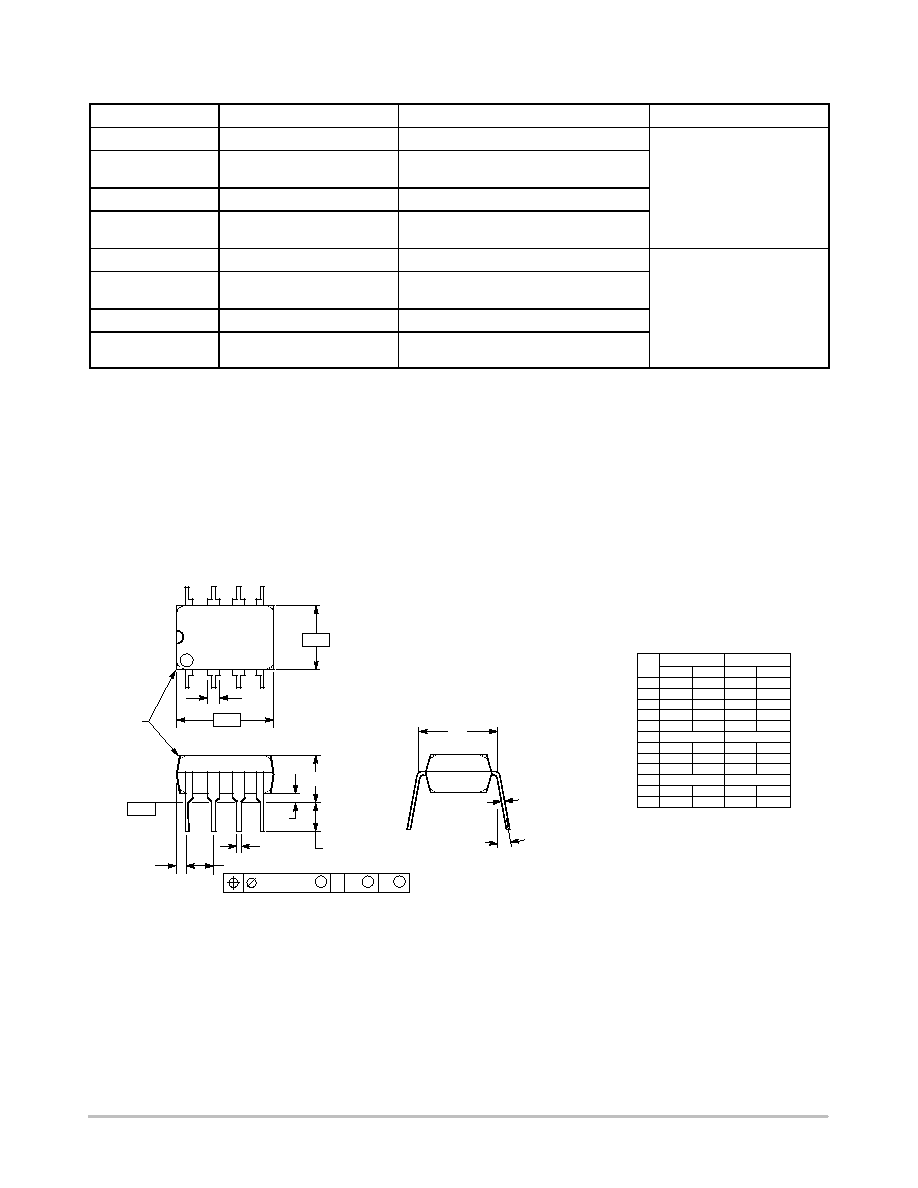
PACKAGE DIMENSIONS
PDIP-8
P SUFFIX
CASE 626-05
ISSUE L
NOTES:
1. DIMENSION L TO CENTER OF LEAD WHEN
FORMED PARALLEL.
2. PACKAGE CONTOUR OPTIONAL (ROUND OR
SQUARE CORNERS).
3. DIMENSIONING AND TOLERANCING PER ANSI
Y14.5M, 1982.
1
4
5
8
F
NOTE 2
-A-
-B-
-T-
SEATING
PLANE
H
J
G
D
K
N
C
L
M
M
A
M
0.13 (0.005)
B
M
T
DIM
MIN
MAX
MIN
MAX
INCHES
MILLIMETERS
A
9.40
10.16
0.370
0.400
B
6.10
6.60
0.240
0.260
C
3.94
4.45
0.155
0.175
D
0.38
0.51
0.015
0.020
F
1.02
1.78
0.040
0.070
G
2.54 BSC
0.100 BSC
H
0.76
1.27
0.030
0.050
J
0.20
0.30
0.008
0.012
K
2.92
3.43
0.115
0.135
L
7.62 BSC
0.300 BSC
M
---
10
---
10
N
0.76
1.01
0.030
0.040
_
_
NCP1653, NCP1653A
http://onsemi.com
19
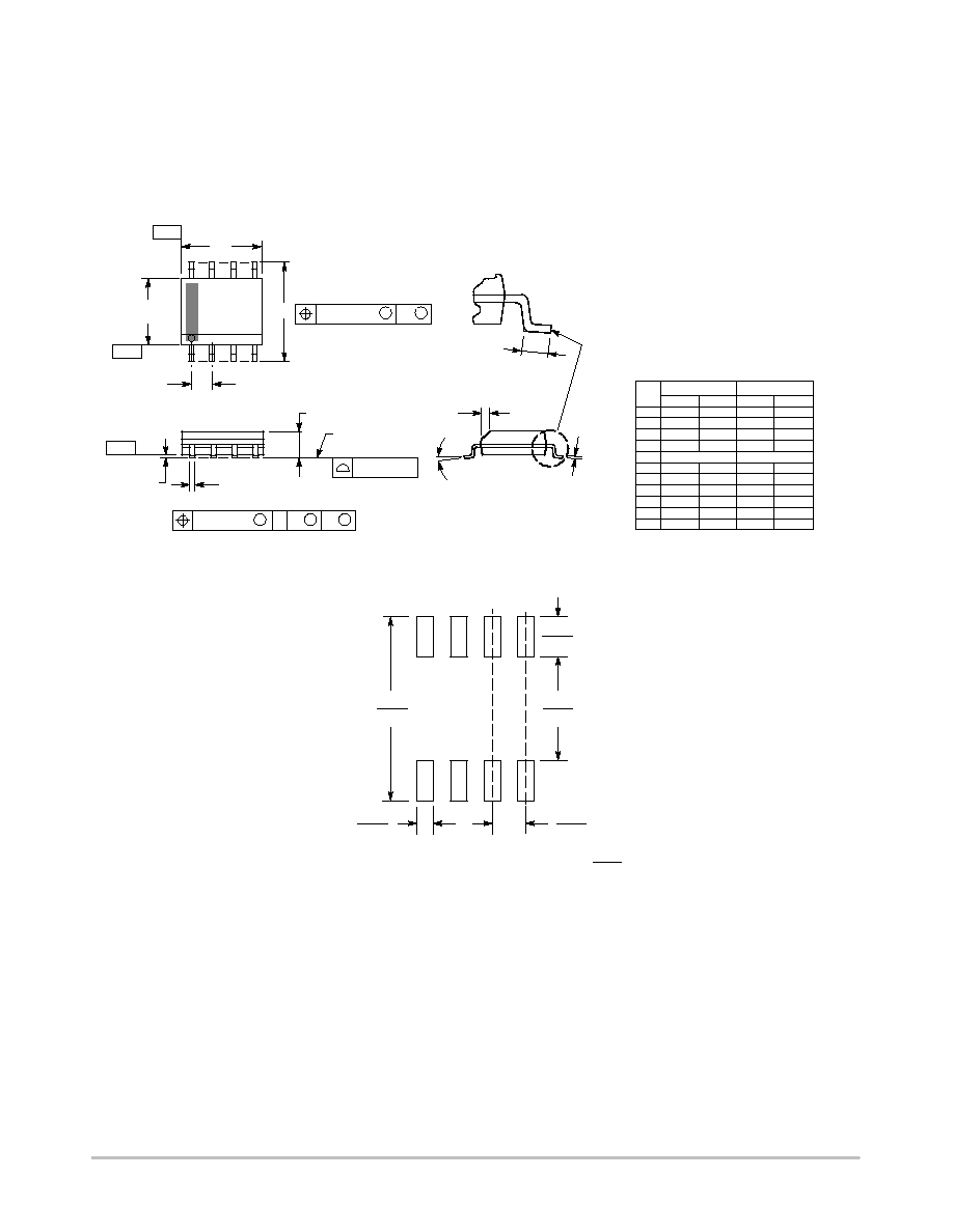
PACKAGE DIMENSIONS
SO-8
D SUFFIX
CASE 751-07
ISSUE AG
SEATING
PLANE
1
4
5
8
N
J
X 45
_
K
NOTES:
1. DIMENSIONING AND TOLERANCING PER
ANSI Y14.5M, 1982.
2. CONTROLLING DIMENSION: MILLIMETER.
3. DIMENSION A AND B DO NOT INCLUDE
MOLD PROTRUSION.
4. MAXIMUM MOLD PROTRUSION 0.15 (0.006)
PER SIDE.
5. DIMENSION D DOES NOT INCLUDE DAMBAR
PROTRUSION. ALLOWABLE DAMBAR
PROTRUSION SHALL BE 0.127 (0.005) TOTAL
IN EXCESS OF THE D DIMENSION AT
MAXIMUM MATERIAL CONDITION.
6. 751-01 THRU 751-06 ARE OBSOLETE. NEW
STANDARD IS 751-07.
A
B
S
D
H
C
0.10 (0.004)
DIM
A
MIN
MAX
MIN
MAX
INCHES
4.80
5.00
0.189
0.197
MILLIMETERS
B
3.80
4.00
0.150
0.157
C
1.35
1.75
0.053
0.069
D
0.33
0.51
0.013
0.020
G
1.27 BSC
0.050 BSC
H
0.10
0.25
0.004
0.010
J
0.19
0.25
0.007
0.010
K
0.40
1.27
0.016
0.050
M
0
8
0
8
N
0.25
0.50
0.010
0.020
S
5.80
6.20
0.228
0.244
-X-
-Y-
G
M
Y
M
0.25 (0.010)
-Z-
Y
M
0.25 (0.010)
Z
S
X
S
M
_
_
_
_
1.52
0.060
7.0
0.275
0.6
0.024
1.270
0.050
4.0
0.155
mm
inches
SCALE 6:1
*For additional information on our Pb-Free strategy and soldering
details, please download the ON Semiconductor Soldering and
Mounting Techniques Reference Manual, SOLDERRM/D.
SOLDERING FOOTPRINT*

NCP1653, NCP1653A
http://onsemi.com
20
ON Semiconductor and are registered trademarks of Semiconductor Components Industries, LLC (SCILLC). SCILLC reserves the right to make changes without further notice
to any products herein. SCILLC makes no warranty, representation or guarantee regarding the suitability of its products for any particular purpose, nor does SCILLC assume any
liability arising out of the application or use of any product or circuit, and specifically disclaims any and all liability, including without limitation special, consequential or incidental
damages. "Typical" parameters which may be provided in SCILLC data sheets and/or specifications can and do vary in different applications and actual performance may vary over
time. All operating parameters, including "Typicals" must be validated for each customer application by customer's technical experts. SCILLC does not convey any license under
its patent rights nor the rights of others. SCILLC products are not designed, intended, or authorized for use as components in systems intended for surgical implant into the body,
or other applications intended to support or sustain life, or for any other application in which the failure of the SCILLC product could create a situation where personal injury or death
may occur. Should Buyer purchase or use SCILLC products for any such unintended or unauthorized application, Buyer shall indemnify and hold SCILLC and its officers, employees,
subsidiaries, affiliates, and distributors harmless against all claims, costs, damages, and expenses, and reasonable attorney fees arising out of, directly or indirectly, any claim of
personal injury or death associated with such unintended or unauthorized use, even if such claim alleges that SCILLC was negligent regarding the design or manufacture of the part.
SCILLC is an Equal Opportunity/Affirmative Action Employer. This literature is subject to all applicable copyright laws and is not for resale in any manner.
PUBLICATION ORDERING INFORMATION
N. American Technical Support: 800-282-9855 Toll Free
USA/Canada
Japan: ON Semiconductor, Japan Customer Focus Center
2-9-1 Kamimeguro, Meguro-ku, Tokyo, Japan 153-0051
Phone: 81-3-5773-3850
NCP1653/D
The product described herein (NCP1653) may be covered by one or more of the following U.S. patents: 6,362,067. There may be other patents pending.
LITERATURE FULFILLMENT:
Literature Distribution Center for ON Semiconductor
P.O. Box 61312, Phoenix, Arizona 85082-1312 USA
Phone: 480-829-7710 or 800-344-3860 Toll Free USA/Canada
Fax: 480-829-7709 or 800-344-3867 Toll Free USA/Canada
Email: orderlit@onsemi.com
ON Semiconductor Website: http://onsemi.com
Order Literature: http://www.onsemi.com/litorder
For additional information, please contact your
local Sales Representative.