
©
Semiconductor Components Industries, LLC, 2003
May, 2003 - Rev. 4
1
Publication Order Number:
NCP1800/D
NCP1800
Single-Cell Lithium Ion
Battery Charge Controller
The NCP1800 is a constant current, constant voltage (CCCV)
lithium ion battery charge controller. The external sense resistor sets
the full charging current, and the termination current is 10% of the full
charge current (0.1 C). The voltage is regulated at
±
1% during the
final charge stage. There is virtually zero drain on the battery when the
input power is removed.
Features
∑
Integrated Voltage and Programmable Current Regulation
∑
Integrated Cell Conditioning for Deeply Discharged Cell
∑
Integrated End of Charge Detection
∑
Better than 1% Voltage Regulation
∑
Charger Status Output for LED or Host Processor Interface
∑
Charge Interrupt Input
∑
Safety Shutoff for Removal of Battery
∑
Adjustable Charge Current Limit
∑
Input Over and Under Voltage Lockout
∑
Micro8 Package
Applications
∑
Cellular Phones, PDAs
∑
Handheld Equipment
∑
Battery Operated Portable Devices
Figure 1. Typical Application
NCP1800
V
CC
CFLG
COMP/
DIS
ISNS
VSNS
ISEL
OUT
R
SNS
R
COMP
C
out
R
ISEL
60 k
Host or LED
Host
Processor
C
COMP
V
in
GND
C
in
PMOS/Schottky (FETKY
t
): NTHD4P02FT1 (ChipFET
t
)
PMOS: NTGS3441T1 (TSOP 6)
Schottky: MBRM130L
R
COMP
= 15
W
, C
COMP
= 560 nF
Micro8
t
CASE 846A
DM SUFFIX
1
8
PIN CONNECTIONS AND
MARKING DIAGRAM
ISNS
OUT
ISEL
COMP/DIS
GND
V
CC
CFLG
VSNS
180X
AY
W
Device
Package
Shipping
ORDERING INFORMATION
NCP1800DM41R2
Micro8
4000 Units/Reel
1
8
2
3
4
7
6
5
http://onsemi.com
X = A for 41 Device
B for 42 Device
A = Assembly Location
L
= Wafer Lot
Y = Year
W = Work Week
NCP1800DM42R2
Micro8
4000 Units/Reel

NCP1800
http://onsemi.com
2
EOC
Detect
Pre CHG
Complete
V
SNS
Overvoltage
GND
COMP/DIS
CFLG
R
ISEL
ISEL
V
CC
I
SNS
EOC REF
Input UV
Lockout
Input OV
Lockout
I
REF
OUT
Figure 2. NCP1800 Internal Block Diagram
V
SNS
CC
CV
V
REF
Chip
Enable
V
REF
V
REF
V
REF
V
REF
V
REF
LOGIC
C
in
Active Pullup
V
REF
R
SNS
C
out
CONTROL
PIN FUNCTION DESCRIPTIONS
Pin
Symbol
Description
1
I
SNS
This is one of the inputs to the current regulator and the end-of-charge comparator.
2
ISEL
A resistor from this pin to ground pin sets the full charging current regulation level.
3
COMP/DIS
This is a multifunctional pin that is used for compensation and can be used to interrupt charge with an
open drain/collector output from a microcontroller. When this pin is pulled to ground, the charge
current is interrupted.
4
GND
This is the ground pin of the IC.
5
V
SNS
This is an input that is used to sense battery voltage and is the other input to the current regulator. It
also serves as the input to the battery overvoltage comparator.
6
CFLG
An open drain output that indicates the battery charging status.
7
V
CC
This is a multifunctional pin that powers the device and senses for over and undervoltage conditions.
8
OUT
This is a current source driver for the pass transistor.
NCP1800
http://onsemi.com
3
MAXIMUM RATINGS
Rating
Symbol
Value
Unit
Supply Voltage
V
CC
16
V
Voltage Range for:
VSNS Input
ISNS Input
COMP/DIS Input
ISEL Input
CFLG Output
Out Output
-
-0.3 to 6.0
-0.3 to 6.0
-0.3 to 6.0
-0.3 to 6.0
-0.3 to 6.0
-0.3 to V
CC
V
OUT Sink Current
Io
20
mA
Thermal Resistance, Junction to Air
R
q
JA
240
∞
C/W
Operating Ambient Temperature
T
A
-20 to +85
∞
C
Operating Junction Temperature
T
J
-20 to +150
∞
C
Storage Temperature
T
stg
-55 to +150
∞
C
ATTRIBUTES
Characteristic
Value
ESD Protection
Human Body Model (HBM) per JEDEC standard JESD22-A114
Machine Model (MM) per JEDEC standard JESD22-A114
2 kV
200 V
Moisture Sensitivity, Indefinite Time Out of Drypack (Note 1)
Level 1
Transistor Count
1015
Latch-up Current Maximum Rating per JEDEC standard JESD78
150 mA
1. For additional information, see Application Note AND8003/D.
ELECTRICAL CHARACTERISTICS
(T
A
= 25
∞
C for typical values, -20
∞
C < T
A
< 85
∞
C for min/max values, unless otherwise noted.)
Characteristic
Symbol
Min
Typ
Max
Unit
Input Supply Voltage (Note 2)
V
CC
2.5
-
16
V
Input Supply Current
I
CC
-
140
250
m
A
Regulated Output Voltage
NCP1800DM41
V
REG
4.059
4.1
4.141
V
Regulated Out ut Voltage
NCP1800DM41
NCP1800DM42
V
REG
4.059
4.158
4.1
4.2
4.141
4.242
V
Full-Charge Current Reference Voltage
V
CC
= 6.0 V, 3.0 V
t
V
SNS
t
4.2 V, R
ISEL
= 60 K
W,
T
A
= 25
∞
C
V
FCHG
210
240
270
mV
Full-Charge Current Reference Voltage Temperature Coefficient
V
CC
= 6.0 V, 3.0 V
t
V
SNS
t
4.2 V, R
ISEL
= 60 K
W
TCV
FCHG
-
-0.163
-
%/
∞
C
Pre-Charge Current Reference Voltage
V
CC
= 6.0 V, V
SNS
t
3.0 V, R
ISEL
= 60 K
W,
T
A
= 25
∞
C
V
PCHG
13.2
24
34.8
mV
Pre- Charge Current Reference Voltage Temperature Coefficient
V
CC
= 6.0 V, V
SNS
t
3.0 V, R
ISEL
= 60 K
W
TCV
PCHG
-
-0.180
-
%/
∞
C
Pre-Charge Threshold Voltage
NCP1800DM41
NCP1800DM42
V
PCTH
2.78
2.85
2.93
3.0
3.08
3.15
V
V
CC
Under Voltage Lockout Voltage
V
UVLO
3.43
3.56
3.69
V
Hysteresis of V
CC
Under Voltage Lockout (V
UVLO
), T
A
= 25
∞
C
-
90
150
195
mV
Hysteresis of V
CC
Under Voltage Lockout Voltage (V
UVLO
) Temperature
Coefficient
-
-
0.261
-
%/
∞
C
End-of-Charge Voltage Reference
V
CC
= 6.0 V, V
SNS
u
4.2 V, R
ISEL
= 60 K
W,
T
A
= 25
∞
C
V
EOC
20
24
28
mV
End-of-Charge Voltage Reference Temperature Coefficient
V
CC
= 6.0 V, V
SNS
u
4.2 V, R
ISEL
= 60 K
W
TCV
EOC
-
-0.160
-
%/
∞
C
2. See the "External Adaptor Power Supply Voltage Selection" section of the application note to determine the minimum voltage of the charger
power supplies.
NCP1800
http://onsemi.com
4
ELECTRICAL CHARACTERISTICS (continued)
(T
A
= 25
∞
C for typical values, -20
∞
C < T
A
< 85
∞
C for min/max values, unless otherwise noted.)
Characteristic
Symbol
Min
Typ
Max
Unit
Charge Disable Threshold Voltage (I
COMP
= 100
m
A min.)
V
CDIS
-
-
0.08
V
V
CC
Over Voltage Lockout
V
OVLO
6.95
7.20
7.45
V
Hysteresis of V
CC
Over Voltage Lockout (V
OVLO
),T
A
= 25
∞
C
-
90
150
180
mV
Hysteresis of V
CC
Over Voltage Lockout (V
OVLO
) Temperature Coefficient
-
-
0.39
-
%/
∞
C
V
SNS
Over Voltage Lockout
NCP1800DM41
NCP1800DM42
V
SOVLO
4.3
4.4
4.4
4.5
4.5
4.6
V
Hysteresis of V
SNS
Over Voltage Lockout (V
SOVLO
), T
A
= 25
∞
C
-
40
70
100
mV
Hysteresis of VSNS Over Voltage Lockout (V
SOVLO
) Temperature Coefficient
T
A
= 25
∞
C
-
-
0.52
-
%/
∞
C
Full Charge Current Range with R
SNS
= 0.4
W
I
REG1
600
-
1000
mA
Full Charge Current Range with R
SNS
= 0.8
W
I
REG2
300
-
600
mA
Battery Drain Current (V
SNS
+ I
SNS
)
V
CC
= Ground, V
SNS
= 4.2 V
I
BDRN
-
-
0.5
m
A
CFLG Pin Output Low Voltage (CFLG = LOW, I
CFLG
= 5.0 mA)
V
CFLGL
-
-
0.35
V
CFLG Pin Leakage Current (CFLG = HIGH)
I
CFLGH
-
-
0.1
m
A
NCP1800
http://onsemi.com
5
V
CC
, INPUT SUPPLY VOLTAGE (V)
V
PCHG
, PRE-CHARGE CURRENT
REFERENCE VOL
T
AGE (mV)
V
PCTH
, PRE-CHARGE THRESHOLD VOL
T
AGE
(V)
7
6
5.5
5
4.5
4
3.5
1
3.5
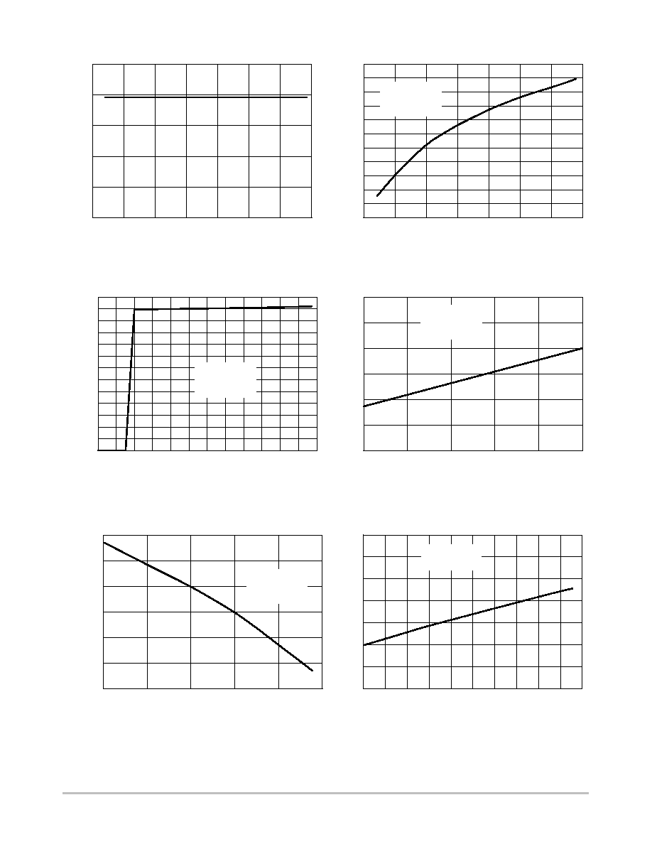
Figure 3. Pre-Charge Threshold Voltage versus
Input Supply Voltage
V
CC
, INPUT SUPPLY VOLTAGE (V)
Figure 4. Pre-Charge Current Reference Voltage
versus Input Supply Voltage
Figure 5. Pre-Charge Current Reference
Voltage versus Battery Voltage
Figure 6. Full-Charge Current Reference Voltage
versus Battery Voltage
3
2.5
2
V
SNS
= 2.5 V
R
ISEL
= 60 k
W
R
SNS
= 0.4
W
7
6
5.5
5
4.5
4
3.5
24.20
24.25
1.5
V
PCHG
, PRE-CHARGE REFERENCE
CURRENT THRESHOLD VOL
T
AGE (mV)
2.9
2.5
2.1
1.7
1.3
0.9
0.5
V
SNS
, BATTERY VOLTAGE (V)
V
FCHG
, FULL-CHARGE CURRENT REFERENCE VOL
T
AGE
(V)
4.2
4.0
3.8
3.6
3.4
3.2
0.24
0.243
V
SNS
, BATTERY VOLTAGE (V)
0.2425
0.241
0.2405
0
26
14
6
4
6.5
6.5
24.30
24.35
24.40
24.45
24.50
24.55
24.60
24.65
24.70
24.75
2
12
10
8
24
16
22
20
18
V
CC
= 5 V
R
ISEL
= 60 k
W
R
SNS
= 0.4
W
V
CC
= 5 V
R
ISEL
= 60 k
W
R
SNS
= 0.4
W
0.2415
0.242
V
CC
, INPUT SUPPLY VOLTAGE (V)
V
EO
C
, END OF CHARGE REFERENCE VOL
T
AGE (mV)
V
FCHG
, CHARGE CURRENT REFERENCE VOL
T
AGE (V)
7
6.5
6
5.5
5
4.5
0.2385
0.2415
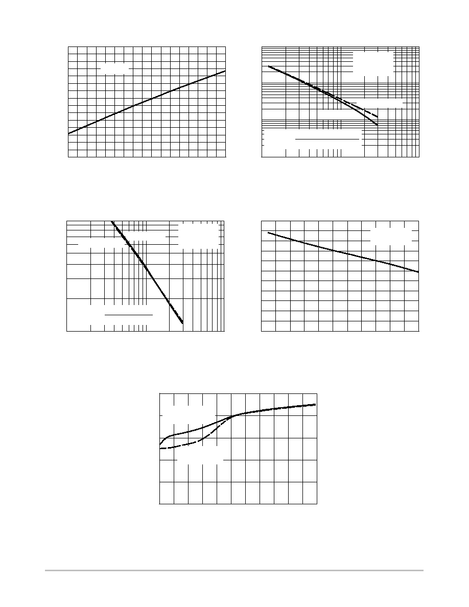
Figure 7. Full-Charge Current Reference
Voltage versus Input Supply Voltage
V
CC
, INPUT SUPPLY VOLTAGE (V)
Figure 8. End of Charge Reference Voltage
versus Input Supply Voltage
0.241
0.2405
7
6.5
6
5.5
5
4.5
23.8
24.5
24.3
24
23.9
0.239
24.4
0.2395
0.24
V
SNS
= 3.6 V
R
ISEL
= 60 k
W
R
SNS
= 0.4
W
24.1
24.2
R
ISEL
= 60 k
W
R
SNS
= 0.4
W
NCP1800
http://onsemi.com
6
0
100
Figure 9. Battery Drain Current versus
Battery Voltage
Figure 10. Pre-Charge Current
versus Current Programming Resistor
Figure 11. Full-Charge Current versus
Current Programming Resistor
Figure 12. V
EOC
/V
FCHG
versus Current
Programming Resistor
I
REG
, FULL-CHARGE CURRENT (mA)
1000
100
10
R
ISEL
, CURRENT PROGRAMMING RESISTANCE (k
W
)
1000
0.11
V
EO
C
/V
FCHG
(V/V)
300
250
200
125
100
50
25
R
ISEL
, CURRENT PROGRAMMING RESISTANCE (k
W
)
0.03
0.02
0.01
I
BDRN
, BA
TTER
Y DRAIN CURRENT (
m
A)
4.1
3.7
3.5
3.3
2.9
2.7
2.5
V
SNS
, BATTERY VOLTAGE (V)
I
PCHG
, PRE-CHARGE CURRENT (mA)
1000
100
10
1
1000
R
ISEL
, CURRENT PROGRAMMING RESISTANCE (k
W
)
100
10
0.2
0.48
0.32
0.24
3.1
3.9
0.28
0.44
0.36
0.40
V
CC
= 0
V
CC
= 5 V
V
SNS
= 2.5 V
R
SNS
= 0.4
W
CALCULATED
MEASURED
V
CC
= 5 V
V
SNS
= 3.6 V
R
SNS
= 0.4
W
CALCULATED
MEASURED
V
CC
= 5 V
R
SNS
= 0.4
W
0.06
0.05
0.04
0.07
0.10
0.09
0.08
75
150 175
225
275
IPCHG
+
(1.19
12e3)
(10
RISEL
RSNS)
IREG
+
(1.19
12e3)
(RISEL
RSNS)
I
CC
, INPUT SUPPL
Y CURRENT (
m
A)
16
12
8
7
6
5
0
250
Figure 13. Input Supply Current versus Input
Supply Voltage
V
CC
, INPUT SUPPLY VOLTAGE (V)
200
150
50
100
V
SNS
= 4.7 V
V
SOVLO
Activated
11
10
9
15
14
13
V
SNS
< V
SOVLO
I
REG
= 0 A
NCP1800
http://onsemi.com
7
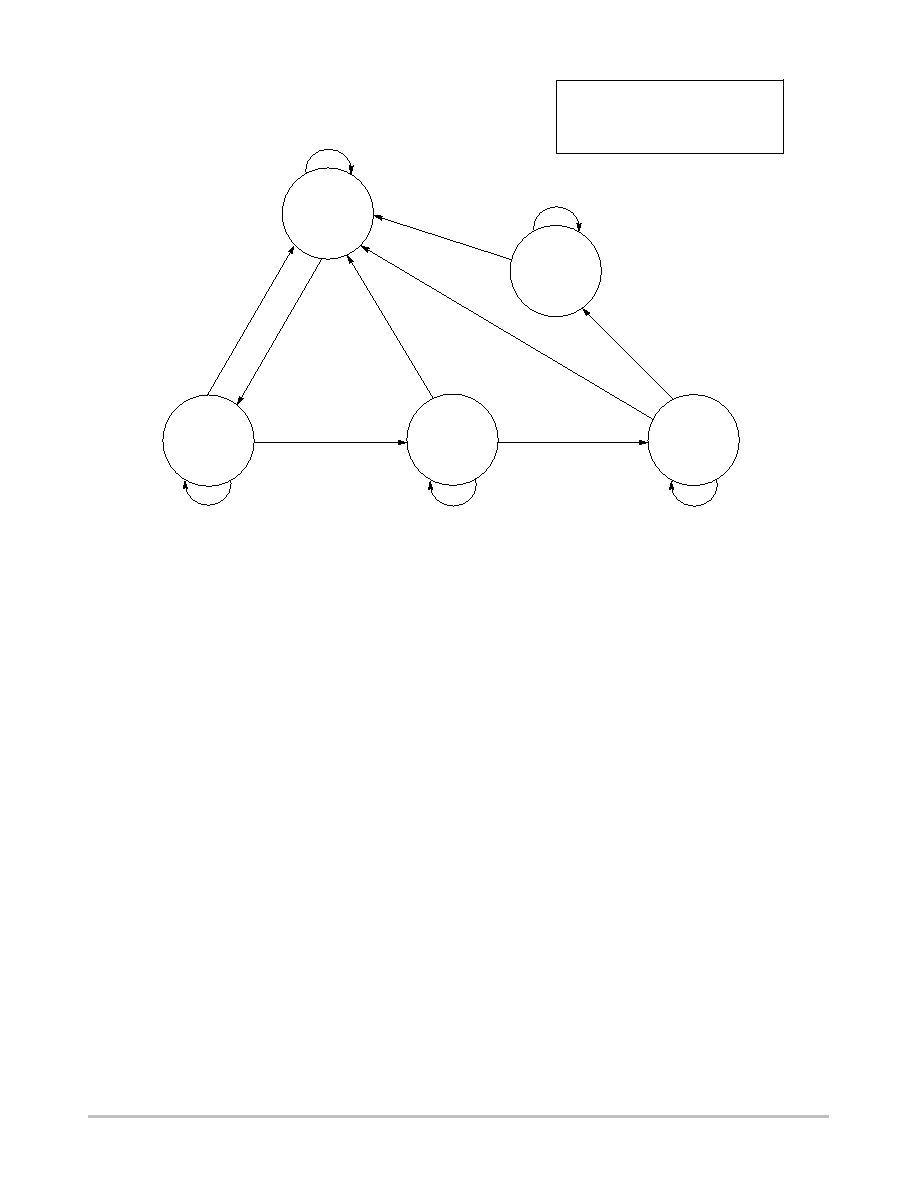
End of Charge
CFLG:Low
OUT:High
Full-Charge
CFLG:High
OUT:1 I
REG
Fault Detected OR V
CDIS
= Low
No Fault Detected
I
SNS
> 0.1 I
REG
V
SNS
< V
REG
Pre- Charge
CFLG:High
OUT:0.1 I
REG
Trickle Charge
CFLG:Low
OUT:V
REG
Final Charge
CFLG:High
OUT:V
REG
V
SNS
< V
PCTH
Fault Modes:
1. Charger Low Output (V
CC
< V
UVLO
)
2. Runaway Charger (V
CC
> V
OVLO
)
3. Battery Removed (V
SNS
> V
SOVLO
)
Figure 14. NCP1800 State Machine Diagram
V
SNS
V
PCTH
V
SNS
V
REG
I
SNS
0.1 I
REG
Fault
Detected OR
V
CDIS
= Low
Fault Detected
OR
V
CDIS
= Low
Fault Detected
OR
V
CDIS
= Low
V
UVLO
< V
CC
< V
OVLO
& V
SNS
< V
SOVLO
NCP1800
http://onsemi.com
8
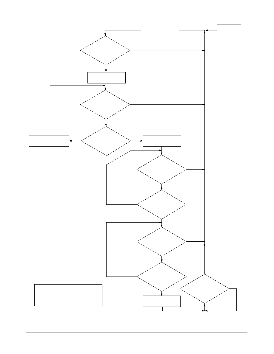
Conditioning Phase
Start
Voltage Regulation Phase
Set CFLG Low
Set I
CHARGE
= I
REG
/10
Set CFLG HIGH
Fault Mode
OR
V
CDIS
= LOW
N
Y
V
SNS
< V
PCTH
Fault Mode
OR
V
CDIS
= LOW
I
SNS
< I
REG
/10
N
Figure 15. NCP1800 Charging Operational Flow Chart
Set CFLG LOW
Y
Fault Mode
OR
V
CDIS
= LOW
N
Y
Set I
CHARGE
= I
REG
N
N
Y
Current Regulation Phase
Fault Mode
OR
V
CDIS
= LOW
V
SNS
> V
REG
N
N
Y
Y
Fault Mode
OR
V
CDIS
= LOW
N
Y
Y
Fault Modes:
1. Charger Low Output (V
CC
< V
UVLO
)
2. Runaway Charger (V
CC
> V
OVLO
)
3. Battery Removed (V
SNS
> V
SOVLO
)
NCP1800
http://onsemi.com
9
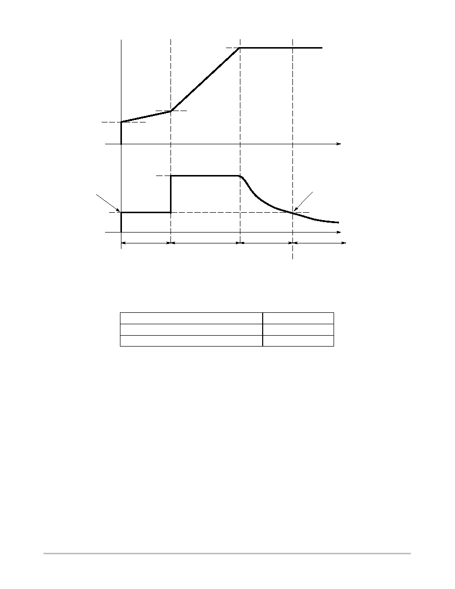
V
REG
V
PCTH
I
REG
0.1 x I
REG
CFLG = Low
(I
SNS
< 0.1 X I
REG
)
Pre-Charge
Phase
Full-Charge
Phase
Final Charge
Phase
Trickle Charge
Phase
Voltage
Current
time
time
Figure 16. Typical Charging Algorithm
CFLG = High
0.9 V
Charge Status
Conditions
CFLG Pin
Pre-Charge, Full-Charge and Final Charge
High-Z
End-of-Charge, Trickle Charge and Faults
Low

NCP1800
http://onsemi.com
10
Operation Descriptions
The NCP1800 is a linear lithium ion (Li-ion) battery
charge controller and provides the necessary control
functions for charging Li-ion batteries precisely and safely.
It features the constant current and constant voltage method
(CCCV) of charging.
Conditioning and Pre-charge Phase
The NCP1800 initiates a charging cycle upon toggling the
COMP/DIS to LOW or application of the valid external
power source (i.e. V
UVLO
t V
CC
t V
OVLO
) with the
Li-ion battery present or when the Li-ion battery is inserted.
Before a charge cycle can begin, the battery conditions are
verified to be within safe limits. The battery will not be
charged when its voltage is less than 0.9 V or higher than
V
SOVLO
.
Li-ion batteries can be easily damaged when fast charged
from a completely discharged state. Also, a fully discharged
Li-ion battery may indicate an abnormal battery condition.
With the built-in safety features of the NCP1800, the Li-ion
battery pre-charges (Pre-Charge Phase) at 10% of the full
rated charging current (I
REG
) when the battery voltage is
lower than V
PCTH
and the CFLG pin is HIGH. Typically, the
battery voltage reaches V
PCTH
in a few minutes and then the
Full Charge phase begins.
Full Charge (Current Regulation) Phase
When the battery voltage reaches V
PCTH
, the NCP1800
begins fast charging the battery with full rate charging
current I
REG
. The NCP1800 monitors the charging current
at the I
SNS
input pin by the voltage drop across a current
sense resistor, R
SNS
, and the charging current is maintained
at I
REG
by the pass transistor throughout the full charge
phase.
I
REG
is determined by R
SNS
and R
ISEL
with the following
formula:
IREG
+
(1.19
12 k)
(RISEL
RSNS)
And with R
ISEL
= 60 k and R
SNS
= 0.4
W, I
REG
= 0.6 A.
Since the external P channel MOSFET is used to regulate
the current to charge the battery and operates in linear mode
as a linear regulator, power is dissipated in the pass
transistor. Designing with a very well regulated external
adaptor (e.g. 5.1 V
±
1%) can help to minimize the heat
dissipation in the pass transistor. Care must be taken in heat
sink designing in enclosed environments such as inside the
battery operated portables or cellular phones.
The Full Charge phase continues until the battery voltage
reaches V
REG
. The NCP1800 comes in two options with
V
REG
thresholds of 4.1 and 4.2 V.
Final Charge (Voltage Regulation) Phase
Once the battery voltage reaches V
REG
, the pass transistor
is controlled to regulate the voltage across the battery and the
Final Charge phase (constant voltage mode) begins. Once
the charger is in the Final Charge phase, the charger
maintains a regulated voltage and the charging current will
begin to decrease and is dependent on the state of the charge
of the battery. As the battery approaches a fully charged
condition, the charge current falls to a very low value.
Trickle Charge Phase
During the Final Charge phase, the charging current
continues to decrease and the NCP1800 monitors the
charging current through the current sense resistor R
SNS
.
When the charging current decreases to such a level that I
SNS
< 0.1 X I
REG
, the CFLG pin is set to LOW and the Trickle
Charge phase begins. The charger stays in the Trickle
Charge phase until any fault modes are detected or the
COMP/DIS pin is pulled low to start over the charging cycle.
NCP1800
http://onsemi.com
11
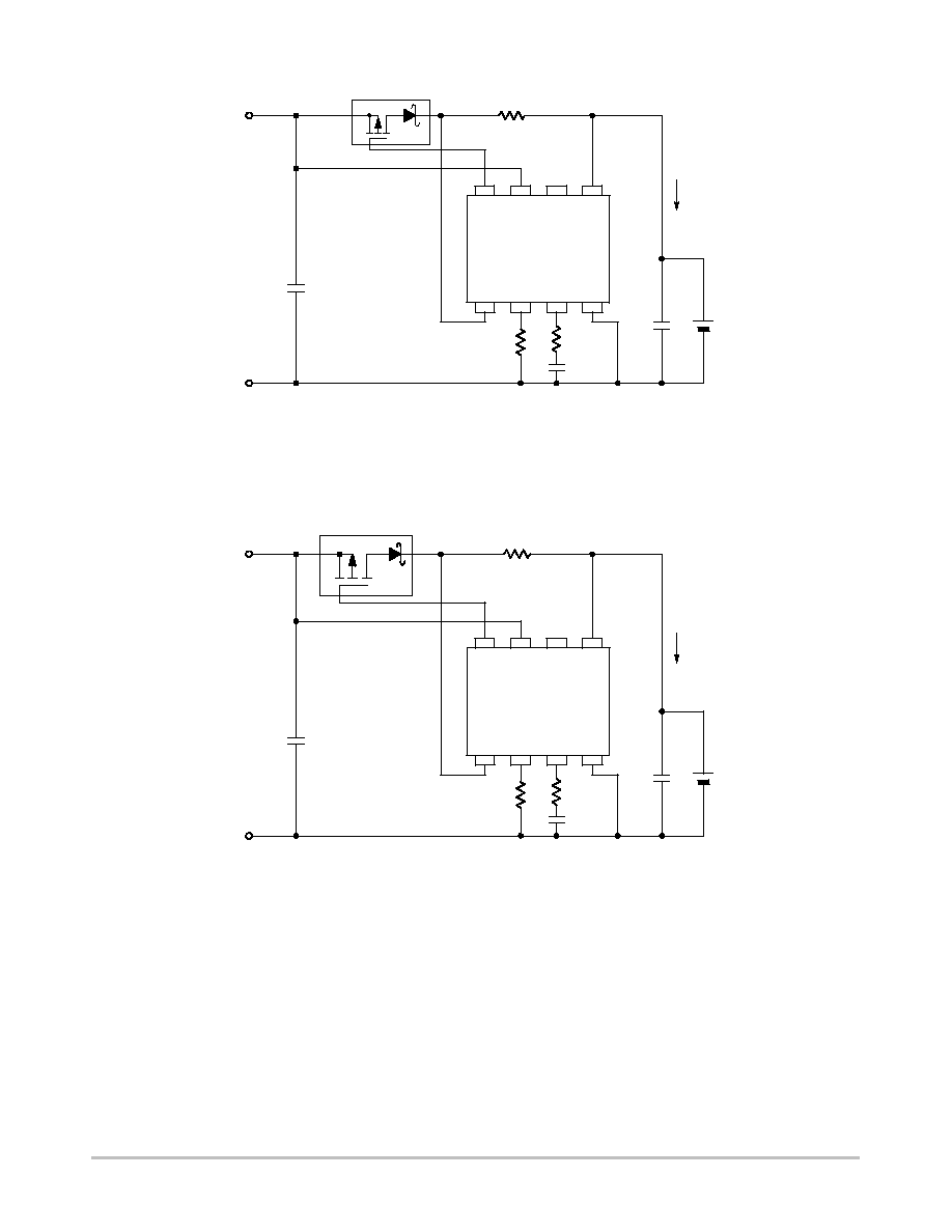
120 mA
GND
C
in
10 n
V
in
= 5.2 V
NTHD4P02FT1
C
out
10
m
R
SNS
2.0
R
ISEL
60 k
560 n
Li-ion
R
COMP
15
C
COMP
OUT V
CC
CFLG V
SNS
I
SNS
I
SEL
COMP/
DIS
GND
Figure 17. Typical Application Circuit for Lower Capacity Batteries (120 mAh shown here)
600 mA
GND
C
in
10 n
V
in
= 5.2 V
NTGS3441T1 & MBRM130L
-OR-
NTHD4P02FT1
C
out
10
m
R
SNS
0.4
R
ISEL
60 k
560 n
Li-ion
R
COMP
15
C
COMP
OUT V
CC
CFLG V
SNS
I
SNS
I
SEL
COMP/
DIS
GND
Figure 18. Typical Application Circuit for Higher Capacity Batteries (600 mAh shown here)
NCP1800
NCP1800

NCP1800
http://onsemi.com
12
Selecting External Components
External Adaptor Power Supply Voltage Selection
Since the NCP1800 is using a linear, charging algorithm,
the efficiency is lower. Adapter voltage selection must be
done carefully in order to minimize the heat dissipation. In
general, the power supply input voltage should be around
5.0 to 6.0 V. The minimum input voltage should be chosen
to minimize the heat dissipation in the system. Excessively
high input voltages can cause too much heat dissipation and
will complicate the thermal design in applications like
cellular phones. With the overvoltage protection feature of
the NCP1800, input voltages higher than 7.0 V will activate
the overvoltage protection circuit and disconnect the power
supply input to the battery and other circuitry.
For the application shown in Figure 18 (assuming
NTGS3441 and MBRM130L):
VIN(min)
u
Li- ion regulated voltage,
VREG
)
(0.6 A)(RDS(ON))
u
4.2 V
)
(0.6 A) (100 m
W
)
)
0.38 V
)
VF of Schottky Diode
)
voltage drop of RSNS
)
(0.6 A) (0.4
W
)
+
4.88 V
]
4.9 V
Therefore, for the application shown in Figure 17
(assuming NTHD4P01FT1):
VIN(min)
u
Li- ion regulated voltage
u
4.2 V
)
(0.12 A)(130m
W
)
)
0.43
)
(0.12 A)(2.0
W
)
+
4.89 V
]
4.9 V
If the output voltage accuracy is 5%, then a typ. 5.2 V
5% output voltage adaptor must be used.
And for a very good regulated adaptor of accuracy 1%, 5.0
V
±
1% output voltage adaptor can then be used. It is obvious
that if tighter tolerance adaptors are used, heat dissipation
can be minimized by using lower nominal voltage adaptors.
Pass Element Selection
The type and size of the pass transistor is determined by
input-output differential voltage, charging current, current
sense resistor and the type of blocking diode used.
The selected pass element must satisfy the following
criteria:
Drop across pass element =
VIN(min)
*
Li- ion regulated voltage
*
VF
*
IREG
RSNS
With:
VIN(min)
+
5.0 V
VREG
+
4.2 V
RSNS
+
0.4
W
IREG
+
0.6 A
Dropout across pass element =
5.0 V
*
4.2 V
*
0.38 V
*
(0.6 A) (0.4
W
)
+
0.18 V
Maximum R
DS(on)
should be less than (0.18 V)/(0.6 A) =
0.3
W at 0.6 A.
VIN(min)
+
5.0 V
VREG
+
4.2 V
RSNS
+
2.0
W
IREG
+
0.12 A
Dropout across pass element = 5.0 V - 4.2 V - 0.43 V -
(0.12)(2.0
W) = 0.13 V.
Therefore, maximum R
DS(on)
should be less than
(0.13 V)/(0.12 A) = 1.08
W at 0.12 A.
External Output Capacitor
Any good quality output filter can be used, independent of
the capacitor's minimum ESR. However, a 10
mF tantalum
capacitor or electrolytic capacitor is recommended at the
output to suppress fast ramping spikes at the V
SNS
input and
to ensure stability for 1.0 A at full range. The capacitor
should be mounted with the shortest possible lead or track
length to the VSNS and GND pins.
Current Sense Resistor
The charging current can be set by the value of the current
sense resistor as in the previous formula. Proper de-rating
is advised when selecting the power dissipation rating of the
resistor. If necessary, R
ISEL
can also be changed for proper
selection of the R
SNS
values. Take note of the recommended
full-char ge current ranges specified in the electrical
characteristics section. Also notice the effect of RISEL on
the accuracy of pre-charge current and end-of-charge
detection as noted in Figures 10 and 12, respectively.
NCP1800
http://onsemi.com
13
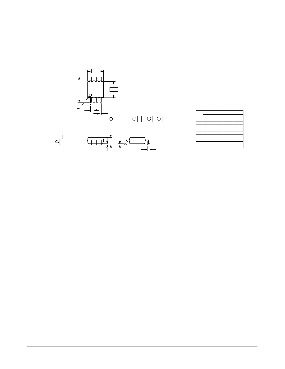
PACKAGE DIMENSIONS
Micro8
DM SUFFIX
CASE 846A-02
ISSUE F
S
B
M
0.08 (0.003)
A
S
T
DIM
MIN
MAX
MIN
MAX
INCHES
MILLIMETERS
A
2.90
3.10
0.114
0.122
B
2.90
3.10
0.114
0.122
C
---
1.10
---
0.043
D
0.25
0.40
0.010
0.016
G
0.65 BSC
0.026 BSC
H
0.05
0.15
0.002
0.006
J
0.13
0.23
0.005
0.009
K
4.75
5.05
0.187
0.199
L
0.40
0.70
0.016
0.028
NOTES:
1. DIMENSIONING AND TOLERANCING PER ANSI
Y14.5M, 1982.
2. CONTROLLING DIMENSION: MILLIMETER.
3. DIMENSION A DOES NOT INCLUDE MOLD FLASH,
PROTRUSIONS OR GATE BURRS. MOLD FLASH,
PROTRUSIONS OR GATE BURRS SHALL NOT
EXCEED 0.15 (0.006) PER SIDE.
4. DIMENSION B DOES NOT INCLUDE INTERLEAD
FLASH OR PROTRUSION. INTERLEAD FLASH OR
PROTRUSION SHALL NOT EXCEED 0.25 (0.010)
PER SIDE.
5. 846A-01 OBSOLETE, NEW STANDARD 846A-02.
-B-
-A-
D
K
G
PIN 1 ID
8 PL
0.038 (0.0015)
-T-
SEATING
PLANE
C
H
J
L

NCP1800
http://onsemi.com
14
ON Semiconductor and are registered trademarks of Semiconductor Components Industries, LLC (SCILLC). SCILLC reserves the right to make
changes without further notice to any products herein. SCILLC makes no warranty, representation or guarantee regarding the suitability of its products for any
particular purpose, nor does SCILLC assume any liability arising out of the application or use of any product or circuit, and specifically disclaims any and all
liability, including without limitation special, consequential or incidental damages. "Typical" parameters which may be provided in SCILLC data sheets and/or
specifications can and do vary in different applications and actual performance may vary over time. All operating parameters, including "Typicals" must be
validated for each customer application by customer's technical experts. SCILLC does not convey any license under its patent rights nor the rights of others.
SCILLC products are not designed, intended, or authorized for use as components in systems intended for surgical implant into the body, or other applications
intended to support or sustain life, or for any other application in which the failure of the SCILLC product could create a situation where personal injury or death
may occur. Should Buyer purchase or use SCILLC products for any such unintended or unauthorized application, Buyer shall indemnify and hold SCILLC
and its officers, employees, subsidiaries, affiliates, and distributors harmless against all claims, costs, damages, and expenses, and reasonable attorney fees
arising out of, directly or indirectly, any claim of personal injury or death associated with such unintended or unauthorized use, even if such claim alleges that
SCILLC was negligent regarding the design or manufacture of the part. SCILLC is an Equal Opportunity/Affirmative Action Employer.
PUBLICATION ORDERING INFORMATION
JAPAN: ON Semiconductor, Japan Customer Focus Center
2-9-1 Kamimeguro, Meguro-ku, Tokyo, Japan 153-0051
Phone: 81-3-5773-3850
ON Semiconductor Website: http://onsemi.com
For additional information, please contact your local
Sales Representative.
NCP1800/D
Literature Fulfillment:
Literature Distribution Center for ON Semiconductor
P.O. Box 5163, Denver, Colorado 80217 USA
Phone: 303-675-2175 or 800-344-3860 Toll Free USA/Canada
Fax: 303-675-2176 or 800-344-3867 Toll Free USA/Canada
Email: ONlit@hibbertco.com
N. American Technical Support: 800-282-9855 Toll Free USA/Canada
ChipFET is a trademark of Vishay Siliconix.
FETKY and Micro8 are trademarks of International Rectifier Corporation.