©
Semiconductor Components Industries, LLC, 2004
November, 2004 - Rev. 7
1
Publication Order Number:
NCP2809/D
NCP2809 Series
NOCAPt 135 mW Stereo
Headphone Power Amplifier
The NCP2809 is a cost-effective stereo audio power amplifier
capable of delivering 135 mW of continuous average power per
channel into 16
W loads.
The NCP2809 audio power amplifier is specifically designed to
provide high quality output power from low supply voltage,
requiring very few external components. Since NCP2809 does not
require bootstrap capacitors or snubber networks, it is optimally
suited for low-power portable systems. NCP2809A has an internal
gain of 0 dB while specific external gain can externally be set with
NCP2809B.
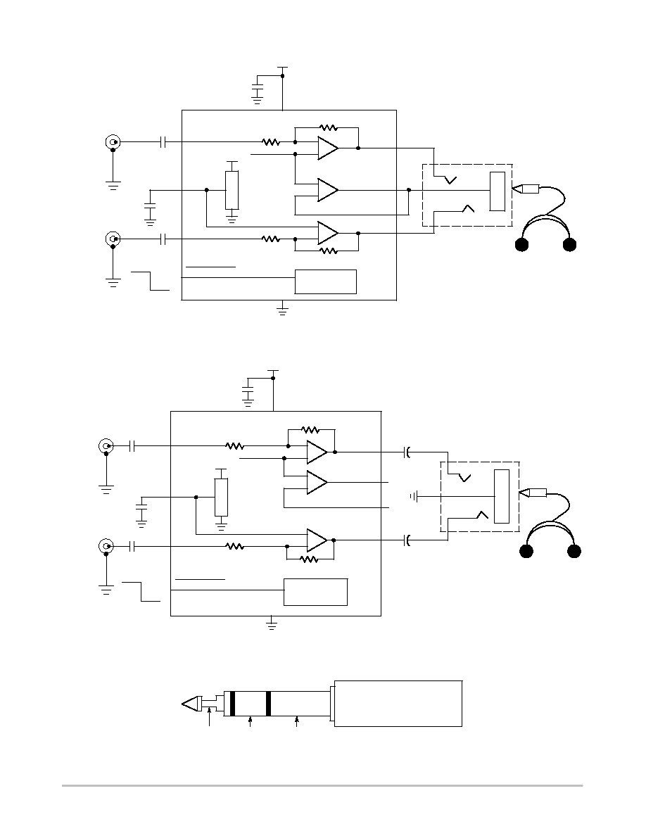
If the application allows it, the virtual ground provided by the
device can be connected to the middle point of the headset (Figure 1).
In such case, the two external heavy coupling capacitors typically
used can be removed. Otherwise, you can also use both outputs in
single ended mode with external coupling capacitors (Figure 43).
Due to its excellent Power Supply Rejection Ratio (PSRR), it can
be directly connected to the battery, saving the use of an LDO.
Features
∑
Pb-Free Package is Available
∑
135 mW to a 16
W Load from a 5.0 V Power Supply
∑
Excellent PSRR (85 dB Typical): Direct Connection to the Battery
∑
"Pop and Click" Noise Protection Circuit
∑
Ultra Low Current Shutdown Mode
∑
2.2 V≠5.5 V Operation
∑
Outstanding Total Harmonics Distortion + Noise (THD+N): Less
than 0.01%
∑
External Turn-on and Turn-off Configuration Capability
∑
Thermal Overload Protection Circuitry
Typical Applications
∑
Cellular Phone
∑
Portable Stereo
∑
MP3 Player
∑
Personal and Notebook Computers
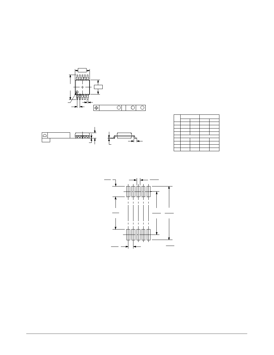
Micro10
DM SUFFIX
CASE 846B
1
10
PIN CONNECTIONS
IN_R
OUT_R
SD
BYP
REF_I
V
M
V
P
1
10
2
3
4
9
8
7
X = E for NCP2809A
MARKING
DIAGRAM
MAx
IN_L
5
OUT_L
6
AYW
X =
C for NCP2809B
A = Assembly Location
Y = Year
W = Work Week
OUT_I
See detailed ordering and shipping information in the package
dimensions section on page 20 of this data sheet.
ORDERING INFORMATION
http://onsemi.com
NCP2809 Series
http://onsemi.com
2
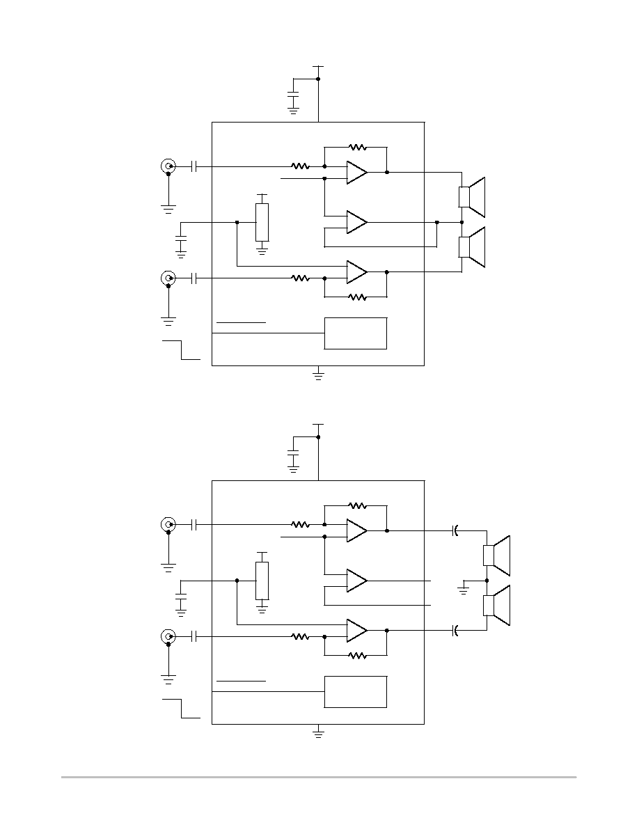
Figure 1. NCP2809A Typical Application Schematic without Output Coupling Capacitor
(NOCAP Configuration)
+
-
+
-
+
-
OUT_L
OUT_I
REF_I
OUT_R
20 k
W
20 k
W
BYPASS
1
m
F
C
S
V
P
V
P
SHUTDOWN
CONTROL
20 k
W
20 k
W
V
M
1
m
F
C
bypass
V
P
V
MC
BRIDGE
BYPASS
SHUTDOWN
IN_R
IN_L
390 nF
C
I
390 nF
C
I
V
IH
V
IL
AUDIO
INPUT
AUDIO
INPUT
Figure 2. NCP2809A Typical Application Schematic with Output Coupling Capacitor
+
-
+
-
+
-
OUT_L
OUT_I
REF_I
OUT_R
BYPASS
1
m
F
C
S
V
P
V
P
SHUTDOWN
CONTROL
20 k
W
20 k
W
V
M
1
m
F
V
P
V
MC
BRIDGE
BYPASS
SHUTDOWN
IN_R
IN_L
390 nF
C
I
390 nF
C
I
V
IH
V
IL
AUDIO
INPUT
AUDIO
INPUT
LEFT
RIGHT
SLEEVE
HEADPHONE JACK
LEFT
RIGHT
SLEEVE
HEADPHONE JACK
20 k
W
20 k
W
NC
NC
220
m
F
C
out
220
m
F
C
out
+
+
TIP
(LEFT)
RING
(RIGHT)
SLEEVE
Figure 3. Typical 3-Wire Headphone Plug

NCP2809 Series
http://onsemi.com
3
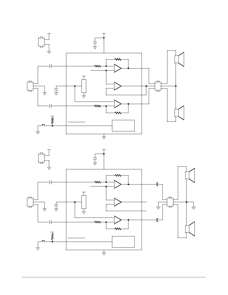
Figure 4. NCP2809B Typical Application Schematic without Output Coupling Capacitor
(NOCAP Configuration)
+
-
+
-
+
-
OUT_L
OUT_I
REF_I
OUT_R
BYPASS
1
m
F
C
S
V
P
V
P
SHUTDOWN
CONTROL
V
M
1
m
F
C
bypass
V
P
V
MC
BRIDGE
BYPASS
SHUTDOWN
IN_R
IN_L
390 nF
C
I
390 nF
C
I
V
IH
V
IL
AUDIO
INPUT
AUDIO
INPUT
Figure 5. NCP2809B Typical Application Schematic with Output Coupling Capacitor
+
-
+
-
+
-
OUT_L
OUT_I
REF_I
OUT_R
BYPASS
1
m
F
C
S
V
P
V
P
SHUTDOWN
CONTROL
V
M
1
m
F
V
P
V
MC
BRIDGE
BYPASS
SHUTDOWN
IN_R
IN_L
390 nF
C
I
390 nF
C
I
V
IH
V
IL
LEFT
RIGHT
SLEEVE
HEADPHONE JACK
LEFT
RIGHT
SLEEVE
HEADPHONE JACK
NC
NC
220
m
F
C
out
220
m
F
C
out
+
+
20 k
W
20 k
W
20 k
W
20 k
W
20 k
W
20 k
W
C
bypass
20 k
W
20 k
W
AUDIO
INPUT
AUDIO
INPUT

NCP2809 Series
http://onsemi.com
4
PIN FUNCTION DESCRIPTION
Pin
Type
Symbol
Description
1
I
IN_R
Negative input of the second amplifier. It receives the audio input signal. Connected to the input
capicator C
in
(NCP2809A) or the external R
in
(NCP2809B).
2
I
SHUTDOWN
The device enters in shutdown mode when a a low level is applied on this pin.
3
I
BYPASS
Bypass capacitor pin which provides the common mode voltage (V
P
/2).
4
O
REF_I
Virtual ground amplifier feed back. This pin sets the stereo headset ground. In order to improve
crosstalk, this pin must be connected as close as possible to the ground connection of the headset
(ideally at the ground pin of the headset connector). When one uses bypassing capacitors, this pin
must be left unconnected.
5
I
IN_L
Negative input of the first amplifier. It receives the audio input signal. Connected to the input
capacitor C
in
(NCP2809A) or the external R
in
(NCP2809B).
6
O
OUT_L
Stereo headset amplifier analog output left. This pin will output the amplified analog signal and,
depending on the application, must be coupled with a capacitor or directly connected to the left
loudspeaker of the headset. This output is able to drive a 16
W
load in a single-ended configuration.
7
I
V
P
Positive analog supply of the cell. Range: 2.2 V ≠ 5.5 V
8
O
OUT_I
Virtual ground for stereo Headset common connection. This pin is directly connected to the
common connection of the headset when use of bypassing capacitor is not required. When one
uses bypassing capacitors, this pin must be left unconnected.
9
I
V
M
Analog Ground
10
O
OUT_R
Stereo headset amplifier analog output right. This pin will output the amplified analog signal and,
depending on the application, must be coupled with a capacitor or directly connected to the right
loudspeaker of the headset. This output is able to drive a 16
W
load in a single-ended configuration.
MAXIMUM RATINGS
(T
A
= +25
∞
C)
Rating
Symbol
Value
Unit
Supply Voltage
V
p
6.0
V
Operating Supply Voltage
O
p
V
p
2.2 to 5.5
V
Input Voltage
V
in
-0.3 to V
CC
+ 0.3
V
Max Output Current
I
out
250
mA
Power Dissipation
P
d
Internally Limited
-
Operating Ambient Temperature
T
A
-40 to +85
∞
C
Max Junction Temperature
T
J
150
∞
C
Storage Temperature Range
T
stg
-65 to +150
∞
C
Thermal Resistance, Junction-to-Air
Micro10
R
q
JA
200
∞
C/W
ESD Protection
Human Body Model (HBM) (Note 1)
Machine Model (MM) (Note 2)
-
8000
200
V
Latch up current at Ta = 85
_
C (Note 3)
±
100
mA
Maximum ratings applied to the device are individual stress limit values (not normal operating conditions) and are not valid simultaneously. If stress
limits are exceeded device functional operation is not implied, damage may occur and reliability may be affected. Functional operation should be
restricted to the Recommended Operating Conditions.
1. Human Body Model, 100 pF discharged through a 1.5 k
W
resistor following specification JESD22/A114 8.0 kV can be applied on OUT_L,
OUT_R, REF_I and OUT_I outputs. For other pins, 2.0 kV is the specified voltage.
2. Machine Model, 200 pF discharged through all pins following specification JESD22/A115.
3. Maximum ratings per JEDEC standard JESD78.
*This device contains 752 active transistors and 1740 MOS gates.
NCP2809 Series
http://onsemi.com
5
ELECTRICAL CHARACTERISTICS
All the parameters are given in the capless configuration (typical application).
The following parameters are given for the NCP2809A and NCP2809B mounted externally with 0 dB gain, unless otherwise noted.
(For typical values T
A
= 25
∞
C, for min and max values T
A
= -40
∞
C to 85
∞
C, T
Jmax
= 125
∞
C, unless otherwise noted.)
Characteristic
Symbol
Conditions
Min
(Note 4)
Typ
Max
(Note 4)
Unit
Supply Quiescent Current
I
DD
V
in
= 0 V, R
L
= 16
W
V
p
= 2.4 V
V
p
= 5.0 V
1.54
1.84
2.8
3.6
mA
Output Offset Voltage
V
off
V
p
= 2.4 V
V
p
= 5.0 V
-25
1.0
+25
mV
Shutdown Current
I
SD
V
p
= 5.0 V
10
600
nA
Shutdown Voltage High (Note 5)
V
SDIH
-
1.2
V
Shutdown Voltage Low
V
SDIL
-
0.4
V
Turning On Time (Note 6)
T
WU
C
by
= 1.0
m
F
285
ms
Turning Off Time (Note 6)
T
SD
C
by
= 1.0
m
F and V
p
= 5.0 V
385
ms
Max Output Swing
V
loadpeak
V
p
= 2.4 V, R
L
= 16
W
V
p
= 5.0 V, R
L
= 16
W
V
p
= 2.4 V, R
L
= 32
W
V
p
= 5.0 V, R
L
= 32
W
0.82
1.94
0.9
2.05
1.04
2.26
V
Max Rms Output Power
P
Orms
V
p
= 2.4 V, R
L
= 16
W
, THD+N<0.1%
V
p
= 5.0 V, R
L
= 16
W
, THD+N<0.1%
V
p
= 2.4 V, R
L
= 32
W
, THD+N<0.1%
V
p
= 5.0 V, R
L
= 32
W
, THD+N<0.1%
24
131
17
80
mW
Voltage Gain
G
NCP2809A only
-0.5
0
+0.5
dB
Crosstalk
CS
f = 1.0 kHz
V
p
= 2.4 V, R
L
= 16
W
, P
out
= 20 mW
V
p
= 2.4 V, R
L
= 32
W
, P
out
= 10 mW
V
p
= 3.0 V, R
L
= 16
W
, P
out
= 30 mW
V
p
= 3.0 V, R
L
= 32
W
, P
out
= 20 mW
V
p
= 5.0 V, R
L
= 16
W
, P
out
= 75 mW
V
p
= 5.0 V, R
L
= 32
W
, P
out
= 50 mW
-63.5
-72.5
-64
-73
-64
-73
dB
Signal to Noise Ratio
SNR
f = 1.0 kHz
V
p
= 2.4 V, R
L
= 16
W
, P
out
= 20 mW
V
p
= 2.4 V, R
L
= 32
W
, P
out
= 10 mW
V
p
= 3.0 V, R
L
= 16
W
, P
out
= 30 mW
V
p
= 3.0 V, R
L
= 32
W
, P
out
= 20 mW
V
p
= 5.0 V, R
L
= 16
W
, P
out
= 75 mW
V
p
= 5.0 V, R
L
= 32
W
, P
out
= 50 mW
88.3
89
90.5
92
95.1
96.1
dB
4. Min/Max limits are guaranteed by production test.
5. At T
A
= -40
∞
C, the minimum value is set to 1.5 V.
6. See page 10 for a theoretical approach to these parameters.

NCP2809 Series
http://onsemi.com
6
ELECTRICAL CHARACTERISTICS
All the parameters are given in the capless configuration (typical application).
The following parameters are given for the NCP2809A and NCP2809B mounted externally with 0 dB gain, unless otherwise noted.
(For typical values T
A
= 25
∞
C, for min and max values T
A
= -40
∞
C to 85
∞
C, T
Jmax
= 125
∞
C, unless otherwise noted.)
Characteristic
Symbol
Conditions
Min
(Note 7)
Typ
Max
(Note 7)
Unit
Positive Supply Rejection Ratio
PSRR V+
R
L
= 16
W
V
pripple_pp
= 200 mV
C
by
= 1.0
m
F
Input Terminated with 10
W
NCP2809A
F = 217 Hz
V
p
= 5.0 V
V
p
= 2.4 V
F = 1.0 kHz
V
p
= 5.0 V
V
p
= 2.4 V
-73
-82
-73
-85
dB
Positive Supply Rejection Ratio
PSRR V+
R
L
= 16
W
V
pripple_pp
= 200 mV
C
by
= 1.0
m
F
Input Terminated with 10
W
NCP2809B
with 0 dB External Gain
F = 217 Hz
V
p
= 5.0 V
V
p
= 2.4 V
F = 1.0 kHz
V
p
= 5.0 V
V
p
= 2.4 V
-80
-82
-81
-81
dB
Efficiency
h
V
P
= 5.0 V, R
L
= 16
W
= 135 mW
63
%
Thermal Shutdown Temperature
(Note 8)
T
sd
-
160
∞
C
Total Harmonic Distortion + Noise
(Note 9)
THD+N
V
P
= 2.4 V, f = 1.0 kHz
R
L
= 16
W
, P
out
= 20 mW
R
L
= 32
W
, P
out
= 15 mW
V
P
= 5.0 V, f = 1.0 kHz
R
L
= 16
W
, P
out
= 120 mW
R
L
= 32
W
, P
out
= 70 mW
0.006
0.004
0.005
0.003
%
7. Min/Max limits are guaranteed by production test.
8. This thermal shutdown is made with an hysteresis function. Typically, the device turns off at 160
∞
C and turns on again when the junction
temperature is less than 140
∞
C.
9. The outputs of the device are sensitive to a coupling capacitor to Ground. To ensure THD+N at very low level for any sort of headset
(16
W
or 32
W)
, outputs (OUT_R, OUT_L, OUT_I and REF_I) must not be grounded with more than 500 pF.
NCP2809 Series
http://onsemi.com
7
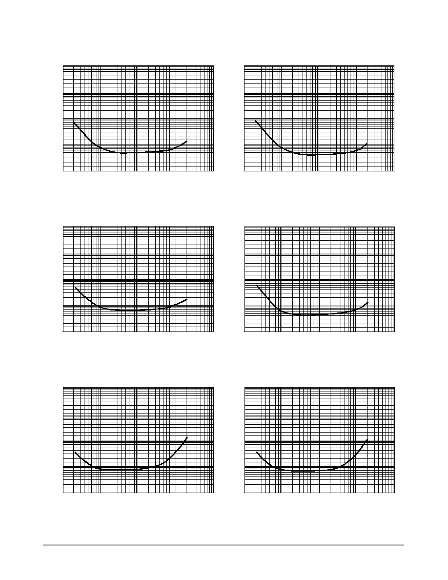
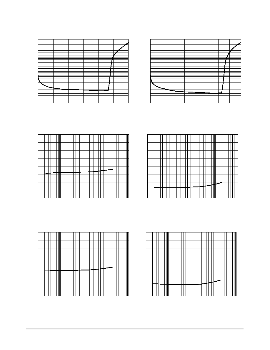
TYPICAL CHARACTERISTICS
0.001
0.01
0.1
1
10
10
100
1000
10000
100000
FREQUENCY (Hz)
THD+N (%)
0.001
0.01
0.1
1
10
10
100
1000
10000
100000
FREQUENCY (Hz)
THD+N (%)
0.001
0.01
0.1
1
10
10
100
1000
10000
100000
FREQUENCY (Hz)
THD+N (%)
0.001
0.01
0.1
1
10
10
100
1000
10000
100000
FREQUENCY (Hz)
THD+N (%)
0.001
0.01
0.1
1
10
10
100
1000
10000
100000
FREQUENCY (Hz)
THD+N (%)
Figure 6. THD+N vs. Frequency
V
p
= 5.0 V, R
L
= 16
W
, P
out
= 75 mW
0.001
0.01
0.1
1
10
10
100
1000
10000
100000
FREQUENCY (Hz)
THD+N (%)
Figure 7. THD+N vs. Frequency
V
p
= 5.0 V, R
L
= 32
W
, P
out
= 50 mW
Figure 8. THD+N vs. Frequency
V
p
= 3.0 V, R
L
= 16
W
, P
out
= 30 mW
Figure 9. THD+N vs. Frequency
V
p
= 3.0 V, R
L
= 32
W
, P
out
= 20 mW
Figure 10. THD+N vs. Frequency
V
p
= 2.4 V, R
L
= 16
W
, P
out
= 20 mW
Figure 11. THD+N vs. Frequency
V
p
= 2.4 V, R
L
= 32
W
, P
out
= 10 mW

NCP2809 Series
http://onsemi.com
8
TYPICAL CHARACTERISTICS
0.001
0.01
0.1
1
10
THD+N (%)
OUTPUT POWER (mW)
10
30
40
50
0
20
0.001
0.01
0.1
1
10
THD+N (%)
OUTPUT POWER (mW)
10
20
30
35
0
5
15
25
0.001
0.01
0.1
1
10
THD+N (%)
OUTPUT POWER (mW)
0.001
0.01
0.1
1
10
0
20
40
60
80
100
120
140
160
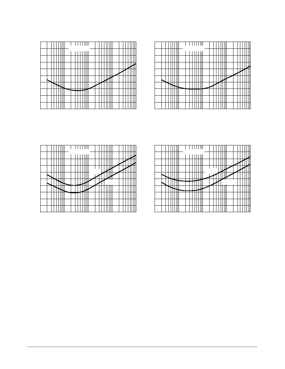
Figure 12. THD+N vs. Power Out
V
p
= 5.0 V, R
L
= 16
W
, 1.0 kHz
Figure 13. THD+N vs. Power Out
V
p
= 5.0 V, R
L
= 32
W
, 1.0 kHz
0
10
20
30
40
50
60
70
80
90
Figure 14. THD+N vs. Power Out
V
p
= 3.3 V, R
L
= 16
W
, 1.0 kHz
Figure 15. THD+N vs. Power Out
V
p
= 3.3 V, R
L
= 32
W
, 1.0 kHz
10
20
30
40
Figure 16. THD+N vs. Power Out
V
p
= 3.0 V, R
L
= 16
W
, 1.0 kHz
Figure 17. THD+N vs. Power Out
V
p
= 3.0 V, R
L
= 32
W
, 1.0 kHz
THD+N (%)
OUTPUT POWER (mW)
0.001
0.01
0.1
1
10
0
THD+N (%)
OUTPUT POWER (mW)
0.001
0.01
0.1
1
10
THD+N (%)
OUTPUT POWER (mW)
0
10
30
40
50
0
20
60
NCP2809 Series
http://onsemi.com
9
TYPICAL CHARACTERISTICS
CROSST
ALK (dB)
FREQUENCY (Hz)
-80
-70
-60
-50
-40
10
100
1000
10000
100000
CROSST
ALK (dB)
FREQUENCY (Hz)
0.001
0.01
0.1
1
10
THD+N (%)
OUTPUT POWER (mW)
0
5
10
15
20
0.001
0.01
0.1
1
10
THD+N (%)
OUTPUT POWER (mW)
0
5
10
15
20
25
30
-80
-70
-60
-50
-40
10
100
1000
10000
100000
CROSST
ALK (dB)
FREQUENCY (Hz)
-80
-70
-60
-50
-40
10
100
1000
10000
100000
CROSST
ALK (dB)
FREQUENCY (Hz)
-80
-70
-60
-50
-40
10
100
1000
10000
100000
Figure 18. THD+N vs. Power Out
V
p
= 2.4 V, R
L
= 16
W
, 1.0 kHz
Figure 19. THD+N vs. Power Out
V
p
= 2.4 V, R
L
= 3.2
W
, 1.0 kHz
Figure 20. Crosstalk
V
p
= 5.0 V, R
L
= 16
W
, P
out
= 75 mW
Figure 21. Crosstalk
V
p
= 5.0 V, R
L
= 32
W
, P
out
= 50 mW
Figure 22. Crosstalk
V
p
= 3.0 V, R
L
= 16
W
, P
out
= 30 mW
Figure 23. Crosstalk
V
p
= 3.0 V, R
L
= 32
W
, P
out
= 20 mW

NCP2809 Series
http://onsemi.com
10
TYPICAL CHARACTERISTICS
-110
-100
-90
-80
-70
-60
-50
-40
-30
-20
-10
PSRR (dB)
FREQUENCY (Hz)
10
100
1000
10000
100000
-110
-100
-90
-80
-70
-60
-50
-40
-30
-20
-10
PSRR (dB)
FREQUENCY (Hz)
10
100
1000
10000
100000
-110
-100
-90
-80
-70
-60
-50
-40
-30
-20
-10
PSRR (dB)
FREQUENCY (Hz)
10
100
1000
10000
100000
Figure 24. Crosstalk
V
p
= 2.4 V, R
L
= 16
W
, P
out
= 20 mW
Figure 25. Crosstalk
V
p
= 2.4 V, R
L
= 32
W
, P
out
= 10 mW
-110
-100
-90
-80
-70
-60
-50
-40
-30
-20
-10
Figure 26. PSRR - Input Grounded with 10
W
V
p
= 2.4 V, V
ripple
= 200 mV pk-pk, R
L
=16
W
CROSST
ALK (dB)
FREQUENCY (Hz)
-80
-70
-60
-50
-40
10
100
1000
10000
100000
CROSST
ALK (dB)
FREQUENCY (Hz)
-80
-70
-60
-50
-40
10
100
1000
10000
100000
PSRR (dB)
FREQUENCY (Hz)
10
100
1000
10000
100000
Figure 27. PSRR - Input Grounded with 10
W
V
p
= 2.4 V, V
ripple
= 200 mV pk-pk, R
L
= 32
W
Figure 28. PSRR - Input Grounded with 10
W
V
p
= 3.0 V, V
ripple
= 200 mV pk-pk, R
L
=16
W
Figure 29. PSRR - Input Grounded with 10
W
V
p
=3.0 V, V
ripple
= 200 mV pk-pk, R
L
= 32
W
NCP2809A
NCP2809A
NCP2809A
NCP2809A

NCP2809 Series
http://onsemi.com
11
TYPICAL CHARACTERISTICS
-110
-100
-90
-80
-70
-60
-50
-40
-30
-20
-10
PSRR (dB)
FREQUENCY (Hz)
10
100
1000
10000
100000
-110
-100
-90
-80
-70
-60
-50
-40
-30
-20
-10
PSRR (dB)
FREQUENCY (Hz)
10
100
1000
10000
100000
-110
-100
-90
-80
-70
-60
-50
-40
-30
-20
-10
PSRR (dB)
FREQUENCY (Hz)
10
100
1000
10000
100000
-110
-100
-90
-80
-70
-60
-50
-40
-30
-20
-10
PSRR (dB)
FREQUENCY (Hz)
10
100
1000
10000
100000
Figure 30. PSRR - Input Grounded with 10
W
V
p
= 3.3 V, V
ripple
= 200 mV pk-pk, R
L
=16
W
Figure 31. PSRR - Input Grounded with 10
W
V
p
= 3.3 V, V
ripple
= 200 mV pk-pk, R
L
= 32
W
Figure 32. PSRR - Input Grounded with 10
W
V
p
= 5.0 V, V
ripple
= 200 mV pk-pk, R
L
=16
W
Figure 33. PSRR - Input Grounded with 10
W
V
p
= 5.0 V, V
ripple
= 200 mV pk-pk, R
L
= 32
W
NCP2809A
NCP2809A
NCP2809A
NCP2809A
NCP2809 Series
http://onsemi.com
12
TYPICAL CHARACTERISTICS
-110
-100
-90
-80
-70
-60
-50
-40
-30
-20
-10
PSRR (dB)
FREQUENCY (Hz)
10
100
1000
10000
100000
-110
-100
-90
-80
-70
-60
-50
-40
-30
-20
-10
PSRR (dB)
FREQUENCY (Hz)
10
100
1000
10000
100000
-110
-100
-90
-80
-70
-60
-50
-40
-30
-20
-10
PSRR (dB)
FREQUENCY (Hz)
10
100
1000
10000
100000
-110
-100
-90
-80
-70
-60
-50
-40
-30
-20
-10
PSRR (dB)
FREQUENCY (Hz)
10
100
1000
10000
100000
Figure 34. PSRR - Input Grounded with 10
W
V
p
= 2.4 V, V
ripple
= 200 mV pk-pk, R
L
=16
W
,
G = 1 (0 dB)
Figure 35. PSRR - Input Grounded with 10
W
V
p
= 5.0 V, V
ripple
= 200 mV pk-pk, R
L
= 16
W
,
G = 1 (0 dB)
Figure 36. PSRR - Input Grounded with 10
W
V
p
= 2.4 V, V
ripple
= 200 mV pk-pk, R
L
=16
W
,
G = 1 (0 dB) and G = 4 (12 dB)
Figure 37. PSRR - Input Grounded with 10
W
V
p
= 5.0 V, V
ripple
= 200 mV pk-pk, R
L
= 16
W
,
G = 1 (0 dB) and G = 4 (12 dB)
NCP2809B
NCP2809B
G = 4
G = 1
G = 4
G = 1
NCP2809B
NCP2809B
NCP2809 Series
http://onsemi.com
13
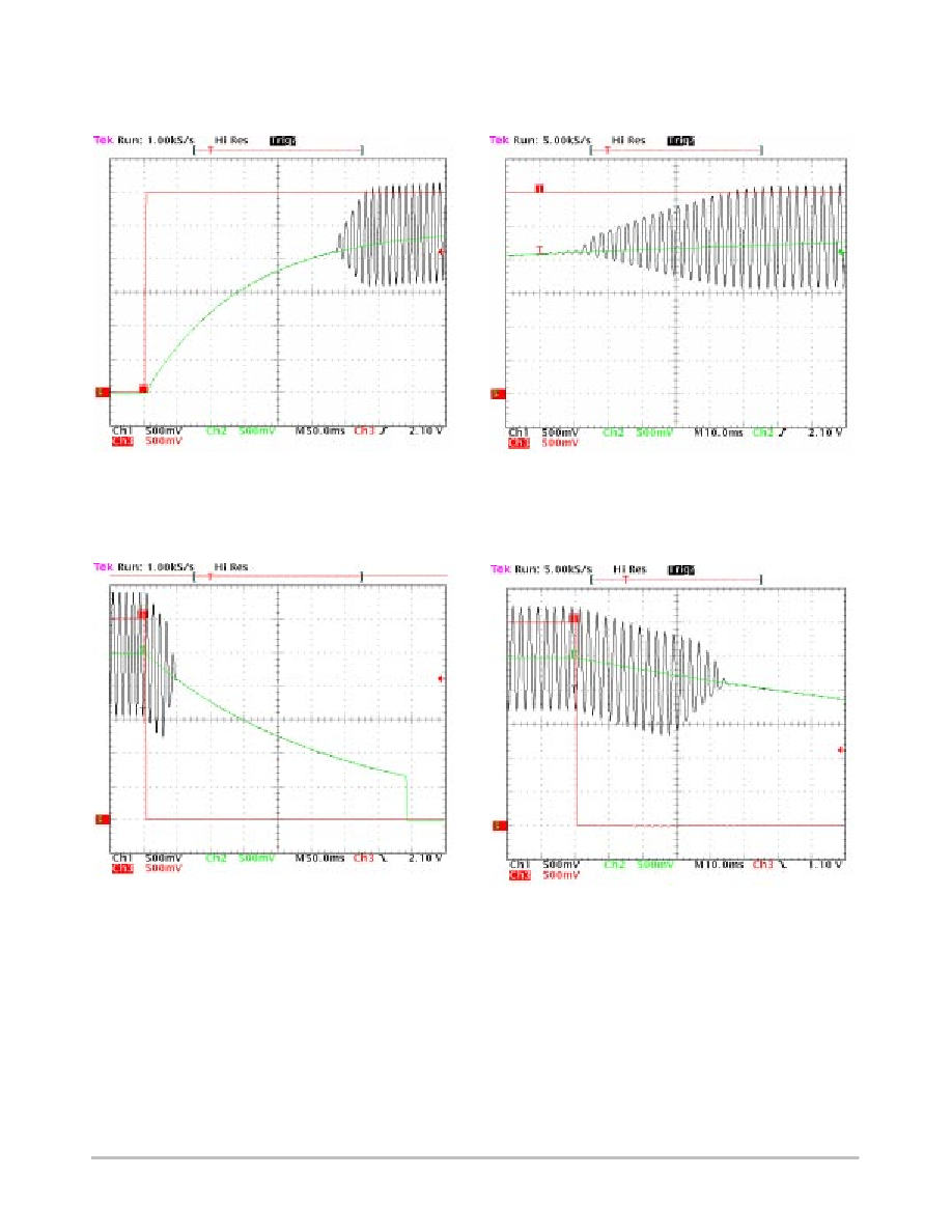
TYPICAL CHARACTERISTICS
Figure 38. Turning≠On Time/V
p
= 5.0 V
and F = 100 Hz
Ch1 = OUT_R, Ch2 = VMC and Ch3 = Shutdown
Figure 39. Turning≠On Time Zoom/V
p
= 5.0 V
and F = 400 Hz
Ch1 = OUT_R, Ch2 = VMC and Ch3 = Shutdown
Figure 40. Turning≠Off Time/V
p
= 5.0 V
and F = 100 Hz
Ch1 = OUT_R, Ch2 = VMC and Ch3 = Shutdown
Figure 41. TurningOff Time Zoom/Vp = 5.0 V
and F = 400 Hz
Ch1 = OUT_R, Ch2 = VMC and Ch3 = Shutdown
NCP2809 Series
http://onsemi.com
14
APPLICATION INFORMATION
Detailed Description
The NCP2809 power audio amplifier can operate from
2.6 V to 5.0 V power supply. It delivers 24 mW
rms
output
power to a 16
W load (V
P
= 2.4 V) and 131 mW
rms
output
power to a 16
W load (V
P
= 5.0 V).
The structure of NCP2809 is basically composed of two
identical internal power amplifiers; NCP2809A has a fixed
internal gain of 0 dB and the gain can be set externally with
the NCP2809B.
Internal Power Amplifier
The output P
mos
and N
mos
transistors of the amplifier are
designed to deliver the specified output power without
clipping. The channel resistance (R
on
) of the N
mos
and P
mos
transistors does not exceed 3.0
W when driving current.
The structure of the internal power amplifier is
composed of three symmetrical gain stages, first and
medium gain stages are transconductance gain stages in
order to maximize bandwidth and DC gain.
Turn-On and Turn-Off Transitions
A Turn-on/off transition is shown in the following plot
corresponding to curves in Figures 38 to 41.
In order to eliminate "pop and click" noises during
transitions, output power in the load must be slowly
established or cut. When logic high is applied to the
shutdown pin, the bypass voltage begins to rise
exponentially and once the output DC level is around the
common mode voltage, the gain is established slowly
(50 ms). This way to turn-on the device is optimized in
terms of rejection of "pop and click" noises.
The device has the same behavior when turned-off by a
logic low on the shutdown pin. During the shutdown mode,
amplifier outputs are connected to the ground.
A theoretical value of turn-on and off times at 25
∞
C is
given by the following formula.
C
by
: Bypass Capacitor
R: Internal 300 k resistor with a 25% accuracy
T
on
= 0.95 * R * C
by
T
off
= R * C
by
* Ln(V
p
/1.4)
Shutdown Function
The device enters shutdown mode when shutdown signal
is low. During the shutdown mode, the DC quiescent
current of the circuit does not exceed 600 nA.
Current Limit Protection Circuitry
The maximum output power of the circuit (P
Orms
=
135 mW, V
P
= 5.0 V, R
L
= 16
W) requires a peak current in
the load of 130 mA.
In order to limit excessive power dissipation in the load
when a short-circuit occurs, the current limit in the load is
fixed to 250 mA. The current in the output MOS transistors
is real-time monitored, and when exceeding 250 mA, the
gate voltage of the corresponding MOS transistor is clipped
and no more current can be delivered.
Thermal Overload Protection Circuitry
Internal amplifiers are switched off when temperature
exceeds 160
∞
C, and will be switched back on only when the
temperature goes below 140
∞
C.
NCP2809 is a stereo power audio amplifier.
If the application requires a Single Ended topology with
output coupling capacitors, then the current provided by
the battery for one output is as following:
∑
V
O
(t) is the AC voltage seen by the load. Here we
consider a sine wave signal with a period T and a peak
voltage V
O
.
∑
R
L
is the load.
T
TIME
T/2
V
O
/R
L
I
p
(t)
So, the total power delivered by the battery to the device is:
PTOT
+
Vp
Ipavg
Ipavg
+
1
2
p
p
0
Vo
RL
sin(t)dt
+
Vo
p
.RL
PTOT
+
Vp.Vo
p
.RL
The power in the load is P
OUT
.
POUT
+
VO2
2RL
NCP2809 Series
http://onsemi.com
15
The dissipated power by the device is
PD
+
PTOT
*
POUT
PD
+
Vo
RL
VP
p *
VO
2
At a given power supply voltage, the maximum power
dissipated is:
PDmax
+
VP2
2
p
2.RL
Of course, if the device is used in a typical stereo
application, each load with the same output power will give
the same dissipated power. Thus the total lost power for the
device is:
PD
+
Vo
RL
2VP
p *
VO
And in this case, the maximum power dissipated will be:
PDmax
+
VP2
p
2.RL
In single ended operation, the efficiency is:
h +
p
.VO
2VP
If the application requires a NOCAP scheme without
output coupling capacitors, then the current provided by
the battery for one output is as following:
∑
V
o
(t) is the AC voltage seen by the load. Here we
consider a sine wave signal with a period T and a peak
voltage V
O
.
∑
R
L
is the load.
T
TIME
T/2
V
O
/R
L
I
p
(t)
So, the total power delivered by the battery to the device is:
PTOT
+
Vp
Ipavg
Ipavg
+
1
p
p
0
Vo
RL
sin(t)dt
+
2Vo
p
.RL
PTOT
+
2Vp.Vo
p
.RL
The power in the load is P
OUT
POUT
+
VO2
2RL
The dissipated power by the device is
PD
+
PTOT
*
POUT
PD
+
Vo
RL
2VP
p *
VO
2
At a given power supply voltage, the maximum power
dissipated is:
PDmax
+
2VP2
p
2.RL
Of course, if the device is used in a typical stereo
application, each load with the same output power will give
the same dissipated power. Thus the total lost power for the
device is:
PD
+
Vo
RL
4VP
p *
VO
And in this case, the maximum power dissipated will be:
PDmax
+
4VP2
p
2.RL
In NOCAP operation, the efficiency is:
h +
p
.VO
4VP
Gain-Setting Selection
With NCP2809 Audio Amplifier family, you can select
a closed-loop gain of 0db for the NCP2809A and an
external gain setting with the NCP2809B. In order to
optimize device and system performance, NCP2809 needs
to be used in low gain configurations. It minimizes THD+N
values and maximizes the signal-to-noise ratio, and the
amplifier can still be used without running into the
bandwidth limitations.
NCP2809A can be used when a 0 dB gain is required.
Adjustable gain is available on NCP2809B.

NCP2809 Series
http://onsemi.com
16
NCP2809 Amplifier External Components
Input Capacitor Selection (C
in
)
The input coupling capacitor blocks the DC voltage at
the amplifier input terminal. This capacitor creates a
high-pass filter with the internal R
internal
resistor of 50 k
W,
the cut-off frequency of which is given by:
fc
+
1
2 *
p
* Rin * Cin
(eq. 1)
The size of the capacitor must be large enough to couple
in low frequencies without severe attenuation. However a
large input coupling capacitor requires more time to reach
its quiescent DC voltage (V
P
/2) and can increase the
turn-on pops.
An input capacitor value of 100 nF performs well in
many applications (With R
internal
=50 k
W).
Bypass Capacitor Selection (C
bypass
)
The bypass capacitor C
by
provides half-supply filtering
and determines how fast the NCP2809 turns on.
A proper supply bypassing is critical for low noise
performance and high power supply rejection ratio.
Moreover, this capacitor is a critical component to
minimize the turn-on pop noise. A 1.0
mF bypass capacitor
value should produce clickless and popless shutdown
transitions. The amplifier is still functional with a 0.1
mF
capacitor value but is more sensitive to "pop and click"
noises.
Thus, for optimized performances, a 1.0
mF ceramic
bypassing capacitor is recommended.
Without Output Coupling Capacitor
As described in Figure 42, the internal circuitry of the
NCP2809 device eliminates need of heavy bypassing
capacitors when connecting a stereo headset with 3
connecting points. This circuitry produces a virtual ground
and does not affect either output power or PSRR.
Additionally, eliminating these capacitors reduces cost and
PCB place.
However, user must take care to the connection between
pin REF_I and ground of the headset: this pin is the ground
reference for the headset. So, in order to improve
crosstalk performances, this pin must be plugged
directly to the ground pin of the headset connector.
With Output Coupling Capacitor
However, when using a low cost jack connector (with
third connection to ground), the headset amplifier requires
very few external components as described in Figure 43.
Only two external coupling capacitors are needed. The
main concern is in output coupling capacitors, because of
the value and consequently the size of the components
required. Purpose of these capacitors is biasing DC voltage
and very low frequency elimination. Both, coupling
capacitor and output load form a high pass filter. Audible
frequency ranges from 20 Hz to 20 kHz, but headset used
in portable appliance has poor ability to reproduce signals
below 75 or 100 Hz. Input coupling capacitor and input
resistance also form a high pass filter. These two first order
filters form a second order high pass filter with the same
-3 dB cut off frequency. Consequently, the following
formula must be respected:
1
2
p
50 k
W
Cin
[
1
2
p
RL
Cout
(eq. 2)
Like for loudspeaker amplifier, the input impedance
value for calculating filters cut off frequency is the
minimum input impedance value at maximum output
volume.
To obtain a frequency equal to when frequency is 5 times
the cut off frequency, attenuation is 0.5 dB. So if we want
a
±
0.5 dB at 150 Hz, we need to have a ≠3 dB cut off
frequency of 30 Hz:
f-3dB
w
1
2
p
RL
Cout
(eq. 3)
Cout
w
1
2
p
RL
f-3dB
(eq. 4)
With R
L
= 16
W, and f
-3dB
= 30 Hz formula (4) shows that
C
out
330
mF.
With C
out
= 220
mF,
±
0.5 dB attenuation frequency will
be 225 Hz with a ≠3.0 dB cut off frequency of 45 Hz.
Following this, the input coupling capacitor choice is
straightforward. Using formula (2) input coupling
capacitor value would be 68 nF for a 220
mF output
coupling capacitor and 100 nF for a 330
mF output coupling
capacitor.
When using the NCP2809 with this configuration, pins
REF_I and OUT_I must be left unconnected
(see Figure 43).
NCP2809 Series
http://onsemi.com
17
Figure 42. Typical Application Schematic Without Output Coupling Capacitor
+
-
+
-
+
-
16
W
16
W
OUT_L
REF_I
OUT_R
20 k
W
20 k
W
BYPASS
1
m
F
C
S
V
P
V
P
+
-
+
-
SHUTDOWN
CONTROL
20 k
W
20 k
W
V
M
C
bypass
1
m
F
V
P
V
MC
BRIDGE
BYPASS
SHUTDOWN
IN_R
IN_L
390 nF
C
I
390 nF
C
I
V
IH
V
IL
AUDIO
INPUT
AUDIO
INPUT
OUT_I
Figure 43. Typical Application Schematic With Output Coupling Capacitor
+
-
+
-
+
-
16
W
16
W
OUT_L
REF_I
OUT_R
20 k
W
20 k
W
BYPASS
1
m
F
C
S
V
P
V
P
+
-
+
-
SHUTDOWN
CONTROL
20 k
W
20 k
W
V
M
C
bypass
1
m
F
V
P
V
MC
BRIDGE
BYPASS
SHUTDOWN
IN_R
IN_L
390 nF
C
I
390 nF
C
I
V
IH
V
IL
AUDIO
INPUT
AUDIO
INPUT
NC
NC
220
m
F
C
out
220
m
F
C
out
+
+
OUT_I
NCP2809 Series
http://onsemi.com
18
DEMONSTRATION BOARD AND LAYOUT GUIDELINES
+
-
+
-
+
-
16
W
16
W
OUT_R
REF_I
OUT_L
20 k
W
20 k
W
BYPASS
1
m
F
C1
V
P
V
P
+
-
+
-
SHUTDOWN
CONTROL
20 k
W
20 k
W
V
M
1
m
F
V
P
V
MC
BRIDGE
BYPASS
SHUTDOWN
IN_L
IN_R
390 nF
C2
390 nF
C4
J3 & U2
10
8
4
6
U1
1
2
3
1
3
2
1
3
2
7
VM1
VM1
VM1
1
3
5
2
J2
J4
V
P
VM1
C3
VM1
VM1
9
V
P
100 k
R1
J1
+
-
+
-
+
-
16
W
16
W
OUT_R
REF_I
OUT_L
20 k
W
20 k
W
BYPASS
1
m
F
C5
V
P
V
P
+
-
+
-
SHUTDOWN
CONTROL
20 k
W
20 k
W
V
M
1
m
F
V
P
V
MC
BRIDGE
BYPASS
SHUTDOWN
IN_L
IN_R
390 nF
C6
390 nF
C8
J9 & U4
10
8
4
6
U3
1
2
3
1
3
2
1
3
2
7
VM2
VM2
VM2
1
3
5
2
J8
J10
V
P
VM2
C7
VM2
VM2
9
V
P
100 k
R2
J7
VM2
VM2
220
m
F
220
m
F
C9
C10
NC
NC
+
+
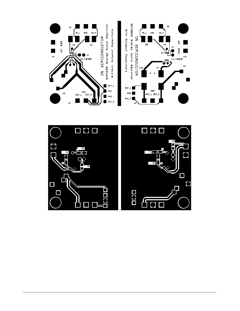
Figure 44. Schematic of the Demonstration Board for Micro10 Device
OUT_I
OUT_I
NCP2809 Series
http://onsemi.com
19
BOTTOM LAYER
TOP LAYER
Figure 45. Demonstration Board for Micro10 Device ≠ PCB Layers
NCP2809 Series
http://onsemi.com
20
Table 1. Bill of Material
Item
Part Description
Ref.
PCB
Footprint
Manufacturer
Manufacturer
Reference
1
NCP2809 Audio Amplifier
U1,U3
Micro10
ON Semiconductor
NCP2809
2
SMD Resistor 100 K
W
R1,R2
0805
Vishay-Draloric
D12CRCW Series
3
Ceramic Capacitor 390 nF 50 V Z5U
C2,C4,
C6,C8
1812
Kemet
C1812C394M5UAC
4
Ceramic Capacitor 1.0
m
F 16 V X7R
Optimized Performance
C1,C3,
C5,C7
1206
Murata
GRM42-6X7R105K16
5
Tantalum Capacitor 220
m
F 10 V
C9,C10
-
Kemet
T495X227010AS
6
I/O Connector. It can be plugged by
BLZ5.08/2 (Weidm¸ller Reference)
J4,J10
-
Weidm¸ller
SL5.08/2/90B
7
I/O Connector. It can be plugged by
BLZ5.08/3 (Weidm¸ller Reference)
J2,J3,
J8,J9
-
Weidm¸ller
SL5.08/3/90B
8
3.5 mm PCB Jack Connector
U2,U4
-
Decelect-Forgos
IES 101-3
9
Jumper Header Vertical Mount
2*1, 2.54 mm
J1,J7
-
-
-
PCB LAYOUT GUIDELINES
How to Optimize the Accuracy of VMC
The main innovation of the NCP2809 stereo NOCAP
audio amplifier is the use of a virtual ground that allows
connecting directly the headset on the outputs of the device
saving DC-blocking output capacitors. In order to have the
best performances in terms of crosstalk, noise and supply
current, the feedback connection on the virtual ground
amplifier is not closed internally. To reach this goal of
excellence, one must connect OUT_I and REF_I as close
as possible from the middle point of the output jack
connector. The most suitable place for this connection is
directly on the pad of this middle point.
How to Optimize THD+N Performances
To get the best THD+N level on the headset speakers, the
traces of the power supply, ground, OUT_R, OUT_L and
OUT_I need the lowest resistance. Thus, the PCB traces for
these nets should be as wide and short as possible.
You need to avoid ground loops, run digital and analog
traces parallel to each other. Due to its internal structure,
the amplifier can be sensitive to coupling capacitors
between Ground and each output (OUT_R, OUT_L and
OUT_I). Avoid running the output traces between two
ground layers or if traces must cross over on different
layers, do it at 90 degrees.
ORDERING INFORMATION
Device
Marking
Package
Shipping
NCP2809ADMR2
MAE
Micro10
4000 Tape & Reel
NCP2809BDMR2
MAC
Micro10
4000 Tape & Reel
NCP2809BDMR2G
MAC
Micro10
(Pb-Free)
4000 Tape & Reel
For information on tape and reel specifications, including part orientation and tape sizes, please refer to our Tape and Reel Packaging
Specifications Brochure, BRD8011/D.
NCP2809 Series
http://onsemi.com
21
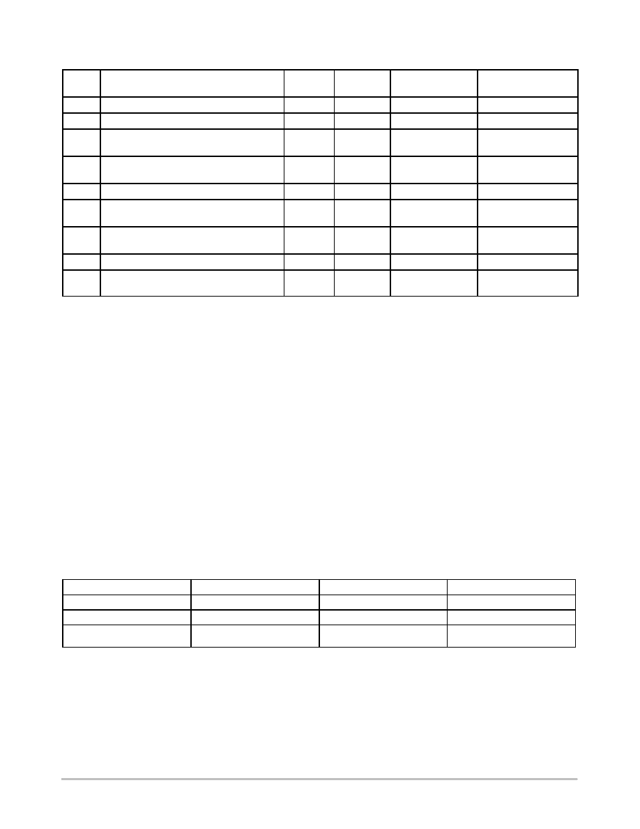
PACKAGE DIMENSIONS
Micro10
DM SUFFIX
CASE 846B-03
ISSUE C
SCALE 8:1
10X
10X
8X
1.04
0.041
0.32
0.0126
5.28
0.208
4.24
0.167
3.20
0.126
0.50
0.0196
mm
inches
S
B
M
0.08 (0.003)
A
S
T
DIM
MIN
MAX
MIN
MAX
INCHES
MILLIMETERS
A
2.90
3.10
0.114
0.122
B
2.90
3.10
0.114
0.122
C
0.95
1.10
0.037
0.043
D
0.20
0.30
0.008
0.012
G
0.50 BSC
0.020 BSC
H
0.05
0.15
0.002
0.006
J
0.10
0.21
0.004
0.008
K
4.75
5.05
0.187
0.199
L
0.40
0.70
0.016
0.028
NOTES:
1. DIMENSIONING AND TOLERANCING PER
ANSI Y14.5M, 1982.
2. CONTROLLING DIMENSION: MILLIMETER.
3. DIMENSION "A" DOES NOT INCLUDE MOLD
FLASH, PROTRUSIONS OR GATE BURRS.
MOLD FLASH, PROTRUSIONS OR GATE
BURRS SHALL NOT EXCEED 0.15 (0.006)
PER SIDE.
4. DIMENSION "B" DOES NOT INCLUDE
INTERLEAD FLASH OR PROTRUSION.
INTERLEAD FLASH OR PROTRUSION
SHALL NOT EXCEED 0.25 (0.010) PER SIDE.
5. 846B-01 OBSOLETE. NEW STANDARD
846B-02
-B-
-A-
D
K
G
PIN 1 ID
8 PL
0.038 (0.0015)
-T-
SEATING
PLANE
C
H
J
L
*For additional information on our Pb-Free strategy and soldering
details, please download the ON Semiconductor Soldering and
Mounting Techniques Reference Manual, SOLDERRM/D.
SOLDERING FOOTPRINT*

NCP2809 Series
http://onsemi.com
22
ON Semiconductor and are registered trademarks of Semiconductor Components Industries, LLC (SCILLC). SCILLC reserves the right to make changes without further notice
to any products herein. SCILLC makes no warranty, representation or guarantee regarding the suitability of its products for any particular purpose, nor does SCILLC assume any
liability arising out of the application or use of any product or circuit, and specifically disclaims any and all liability, including without limitation special, consequential or incidental
damages. "Typical" parameters which may be provided in SCILLC data sheets and/or specifications can and do vary in different applications and actual performance may vary over
time. All operating parameters, including "Typicals" must be validated for each customer application by customer's technical experts. SCILLC does not convey any license under
its patent rights nor the rights of others. SCILLC products are not designed, intended, or authorized for use as components in systems intended for surgical implant into the body,
or other applications intended to support or sustain life, or for any other application in which the failure of the SCILLC product could create a situation where personal injury or death
may occur. Should Buyer purchase or use SCILLC products for any such unintended or unauthorized application, Buyer shall indemnify and hold SCILLC and its officers, employees,
subsidiaries, affiliates, and distributors harmless against all claims, costs, damages, and expenses, and reasonable attorney fees arising out of, directly or indirectly, any claim of
personal injury or death associated with such unintended or unauthorized use, even if such claim alleges that SCILLC was negligent regarding the design or manufacture of the part.
SCILLC is an Equal Opportunity/Affirmative Action Employer. This literature is subject to all applicable copyright laws and is not for resale in any manner.
PUBLICATION ORDERING INFORMATION
N. American Technical Support: 800-282-9855 Toll Free
USA/Canada
Japan: ON Semiconductor, Japan Customer Focus Center
2-9-1 Kamimeguro, Meguro-ku, Tokyo, Japan 153-0051
Phone: 81-3-5773-3850
NCP2809/D
NOCAP is a trademark of Semiconductor Components Industries, LLC (SCILLC).
LITERATURE FULFILLMENT:
Literature Distribution Center for ON Semiconductor
P.O. Box 61312, Phoenix, Arizona 85082-1312 USA
Phone: 480-829-7710 or 800-344-3860 Toll Free USA/Canada
Fax: 480-829-7709 or 800-344-3867 Toll Free USA/Canada
Email: orderlit@onsemi.com
ON Semiconductor Website: http://onsemi.com
Order Literature: http://www.onsemi.com/litorder
For additional information, please contact your
local Sales Representative.