
©
Semiconductor Components Industries, LLC, 2004
November, 2004 - Rev. 8
1
Publication Order Number:
NCP2890/D
NCP2890
1.0 Watt Audio Power
Amplifier
The NCP2890 is an audio power amplifier designed for portable
communication device applications such as mobile phone
applications. The NCP2890 is capable of delivering 1.0 W of
continuous average power to an 8.0
W BTL load from a 5.0 V power
supply, and 320 mW to a 4.0
W BTL load from a 2.6 V power supply.
The NCP2890 provides high quality audio while requiring few
external components and minimal power consumption. It features a
low-power consumption shutdown mode, which is achieved by
driving the SHUTDOWN pin with logic low.
The NCP2890 contains circuitry to prevent from "pop and click"
noise that would otherwise occur during turn-on and turn-off
transitions.
For maximum flexibility, the NCP2890 provides an externally
controlled gain (with resistors), as well as an externally controlled
turn-on and turn-off times (with the bypass capacitor).
Due to its excellent PSRR, it can be directly connected to the
battery, saving the use of an LDO.
This device is available in a 9-Pin Flip-Chip CSP (standard
Tin-Lead and Lead-Free versions) and a Micro8
t package.
Features
∑
Pb-Free Packages are Available
∑
1.0 W to an 8.0
W BTL Load from a 5.0 V Power Supply
∑
Excellent PSRR: Direct Connection to the Battery
∑
"Pop and Click" Noise Protection Circuit
∑
Ultra Low Current Shutdown Mode
∑
2.2 V-5.5 V Operation
∑
External Gain Configuration Capability
∑
External Turn-on and Turn-off Time Configuration Capability
∑
Up to 1.0 nF Capacitive Load Driving Capability
∑
Thermal Overload Protection Circuitry
Typical Applications
∑
Portable Electronic Devices
∑
PDAs
∑
Wireless Phones
9-Pin Flip-Chip CSP
FC SUFFIX
CASE 499E
PIN CONNECTIONS
x
= Specific Device Code,
G or H
A, R
= Assembly Location
Y
= Year
WW, W = Work Week
MARKING
DIAGRAMS
A3
B3
C3
A2
B2
C2
A1
B1
C1
INM
OUTA
INP
VM_P
VM
V
p
BYPASS
OUTB SHUTDOWN
8
7
6
5
1
2
3
4
Micro8
DM SUFFIX
CASE 846A
1
8
SHUTDOWN
BYPASS
INP
INM
OUTB
VM
V
p
OUTA
MAB
RYW
1
8
9-Pin Flip-Chip CSP
Micro8
(Top View)
(Top View)
1
See detailed ordering and shipping information in the package
dimensions section on page 14 of this data sheet.
ORDERING INFORMATION
MAx
AYWW
A1
A3
C1
http://onsemi.com

NCP2890
http://onsemi.com
2
Figure 1. Typical Audio Amplifier Application Circuit with Single Ended Input
+
-
+
-
V
p
INM
V
p
V
p
300 k
W
300 k
W
8
W
OUTA
OUTB
R1
20 k
W
R2
20 k
W
INP
BYPASS
20 k
W
1
m
F
390 nF
VM
VM_P
SHUTDOWN
CONTROL
C
bypass
20 k
W
1
m
F
Cs
SHUTDOWN
Rf
Ri
Ci
AUDIO
INPUT
VIH
VIL
Figure 2. Typical Audio Amplifier Application Circuit with a Differential Input
+
-
+
-
V
p
INM
V
p
V
p
300 k
W
300 k
W
8
W
OUTA
OUTB
R1
20 k
W
R2
20 k
W
INP
BYPASS
20 k
W
1
m
F
390 nF
VM
VM_P
SHUTDOWN
CONTROL
C
bypass
20 k
W
1
m
F
Cs
SHUTDOWN
Rf
Ri
Ci
AUDIO
INPUT
VIH
VIL
20 k
W
390 nF
Ri
Ci
+
-
20 k
W
Rf
This device contains 671 active transistors and 1899 MOS gates.
NCP2890
http://onsemi.com
3
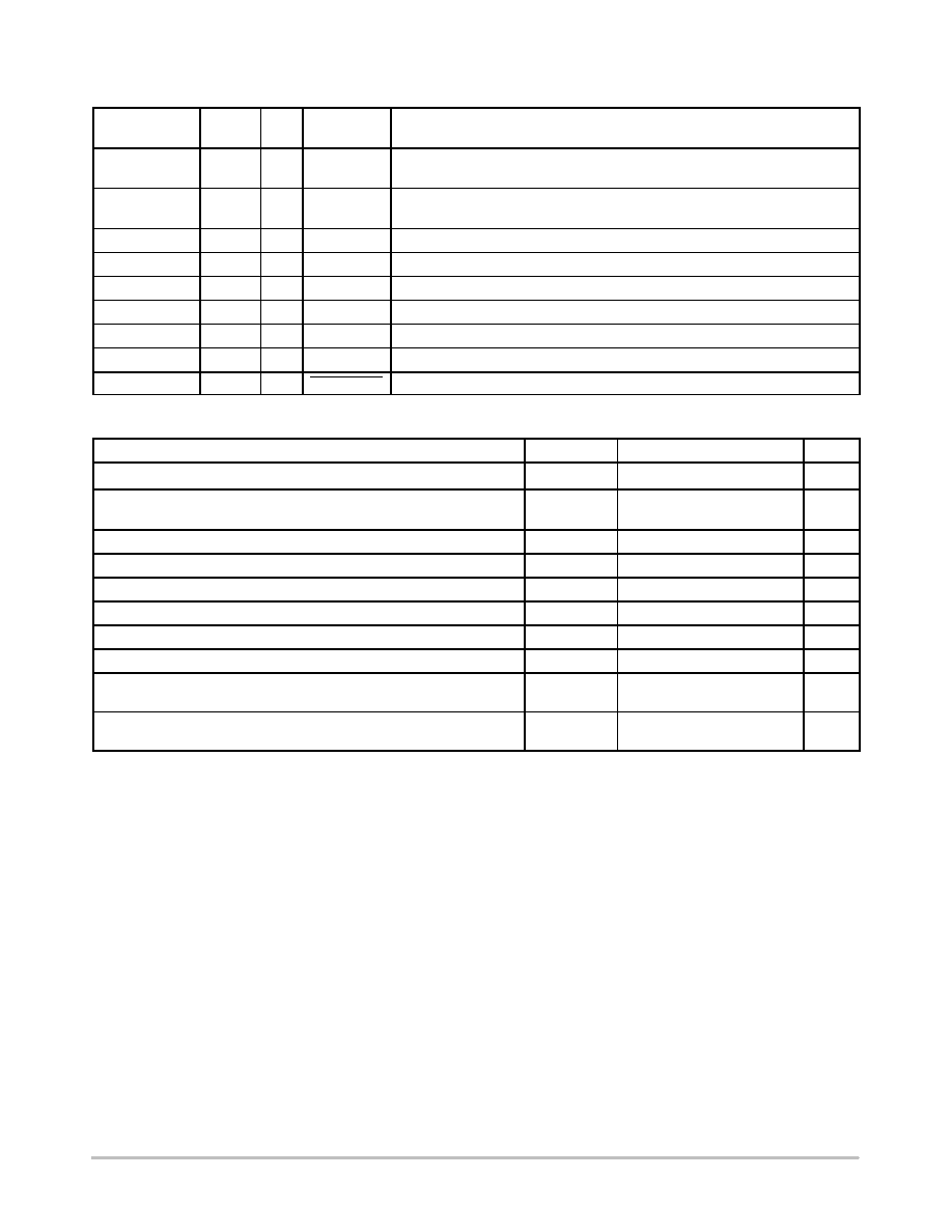
PIN DESCRIPTION
9-Pin Flip-Chip
CSP
Micro8
Type
Symbol
Description
A1
4
I
INM
Negative input of the first amplifier, receives the audio input signal. Connected to
the feedback resistor R
f
and to the input resistor R
in
.
A2
5
O
OUTA
Negative output of the NCP2890. Connected to the load and to the feedback
resistor Rf.
A3
3
I
INP
Positive input of the first amplifier, receives the common mode voltage.
B1
NA
I
VM_P
Power Analog Ground.
B2
7
I
VM
Core Analog Ground.
B3
6
I
V
p
Positive analog supply of the cell. Range: 2.2 V-5.5 V.
C1
2
I
BYPASS
Bypass capacitor pin which provides the common mode voltage (Vp/2).
C2
8
O
OUTB
Positive output of the NCP2890. Connected to the load.
C3
1
I
SHUTDOWN
The device enters in shutdown mode when a low level is applied on this pin.
MAXIMUM RATINGS
(Note 1)
Rating
Symbol
Value
Unit
Supply Voltage
V
p
6.0
V
Operating Supply Voltage
Op Vp
2.2 to 5.5 V
2.0 V = Functional Only
-
Input Voltage
V
in
-0.3 to Vcc +0.3
V
Max Output Current
Iout
500
mA
Power Dissipation (Note 2)
Pd
Internally Limited
-
Operating Ambient Temperature
T
A
-40 to +85
∞
C
Max Junction Temperature
T
J
150
∞
C
Storage Temperature Range
T
stg
-65 to +150
∞
C
Thermal Resistance Junction-to-Air
Micro8
R
q
JA
230
∞
C/W
Thermal Resistance Junction to Air
Micro8
9-Pin Flip-Chip CSP
R
q
JA
230
(Note 3)
C/W
ESD Protection
Human Body Model (HBM) (Note 4)
-
>2500
V
ESD Protection
Human Body Model (HBM) (Note 4)
Machine Model (MM) (Note 5)
>2500
>250
V
Maximum ratings are those values beyond which device damage can occur. Maximum ratings applied to the device are individual stress limit values
(not normal operating conditions) and are not valid simultaneously. If these limits are exceeded, device functional operation is not implied, damage
may occur and reliability may be affected.
1. Maximum electrical ratings are defined as those values beyond which damage to the device may occur at T
A
= +25
∞
C.
2. The thermal shutdown set to 160
∞
C (typical) avoids irreversible damage on the device due to power dissipation. For further information see
page 10.
3. For the 9-Pin Flip-Chip CSP package, the R
q
JA
is highly dependent of the PCB Heatsink area. For example, R
q
JA
can equal 195
∞
C/W with
50 mm
2
total area and also 135
∞
C/W with 500 mm
2
. For further information see page 10. The bumps have the same thermal resistance and
all need to be connected to optimize the power dissipation.
4. Human Body Model, 100 pF discharge through a 1.5 k
W
resistor following specification JESD22/A114.
5. Machine Model, 200 pF discharged through all pins following specification JESD22/A115.

NCP2890
http://onsemi.com
4
ELECTRICAL CHARACTERISTICS
Limits apply for T
A
between -40
∞
C to +85
∞
C (Unless otherwise noted).
Characteristic
Symbol
Conditions
Min
(Note 6)
Typ
Max
(Note 6)
Unit
Supply Quiescent Current
I
dd
V
p
= 2.6 V, No Load
V
p
= 5.0 V, No Load
-
-
1.5
1.7
4
mA
V
p
= 2.6 V, 8
W
V
p
= 5.0 V, 8
W
-
-
1.7
1.9
5.5
Common Mode Voltage
V
cm
-
-
V
p
/2
-
V
Shutdown Current
I
SD
-
-
10
600
nA
Shutdown Voltage High
V
SDIH
-
1.2
-
-
V
Shutdown Voltage Low
V
SDIL
-
-
-
0.4
V
Turning On Time (Note 8)
T
WU
C
by
= 1
m
F
-
285
-
ms
Turning Off Time (Note 8)
T
SD
C
by
= 1
m
F and V
p
= 5.0 V
-
385
-
ms
Output Swing
V
loadpeak
V
p
= 2.6 V, R
L
= 8.0
W
V
p
= 5.0 V, R
L
= 8.0
W
(Note 7)
1.6
4.0
2.12
4.15
-
-
V
Rms Output Power
P
O
V
p
= 2.6 V, R
L
= 4.0
W
THD + N < 0.1%
V
p
= 2.6 V, R
L
= 8.0
W
THD + N < 0.1%
V
p
= 5.0 V, R
L
= 8.0
W
THD + N < 0.1%
-
-
0.36
0.28
1.08
-
-
W
Maximum Power Dissipation (Note 8)
P
Dmax
V
p
= 5.0 V, R
L
= 8.0
W
-
-
0.65
W
Output Offset Voltage
V
OS
V
p
= 2.6 V
V
p
= 5.0 V
-30
30
mV
Signal-to-Noise Ratio
SNR
V
p
= 2.6 V, G = 2.0
10 Hz < F < 20 kHz
V
p
= 5.0 V, G = 10
10 Hz < F < 20 kHz
-
-
84
77
-
-
dB
Positive Supply Rejection Ratio
PSRR V+
G = 2.0, R
L
= 8.0
W
Vp
ripple_pp
= 200 mV
C
by
= 1.0
m
F
Input Terminated with 10
W
F = 217 Hz
V
p
= 5.0 V
V
p
= 3.0 V
V
p
= 2.6 V
F = 1.0 kHz
V
p
= 5.0 V
V
p
= 3.0 V
V
p
= 2.6 V
-
-
-
-
-
-
64
72
73
64
74
75
-
-
-
-
-
-
dB
Efficiency
h
V
p
= 2.6 V, P
orms
= 320 mW
V
p
= 5.0 V, P
orms
= 1.0 W
-
-
48
63
-
-
%
Thermal Shutdown Temperature (Note 9)
T
sd
140
160
180
∞
C
Total Harmonic Distortion
THD
V
p
= 2.6, F = 1.0 kHz
R
L
= 4.0
W,
A
V
= 2.0
P
O
= 0.32 W
V
p
= 5.0 V, F = 1.0 kHz
R
L
= 8.0
W,
A
V
= 2.0
P
O
= 1.0 W
-
-
-
-
-
-
-
0.04
-
-
0.02
-
-
-
-
-
-
-
%
6. Min/Max limits are guaranteed by design, test or statistical analysis.
7. This parameter is not tested in production for 9-Pin Flip-Chip CSP package in case of a 5.0 V power supply.
8. See page 11 for a theoretical approach of these parameters.
9. For this parameter, the Min/Max values are given for information.

NCP2890
http://onsemi.com
5
Typical Performance Characteristics
Figure 1. THD + N versus Frequency
10
100
1000
10,000
100,000
1
0.001
0.1
T
H
D
+ N (%)
FREQUENCY (Hz)
Figure 2. THD + N versus Frequency
10
100
1000
10,000
100,000
1
0.001
0.1
THD + N (%)
FREQUENCY (Hz)
V
p
= 5 V
R
L
= 8
W
P
out
= 250 mW
A
V
= 2
V
p
= 3.3 V
R
L
= 8
W
P
out
= 150 mW
A
V
= 2
Figure 3. THD + N versus Frequency
10
100
1000
10,000
100,000
1
0.001
0.1
THD + N (%)
FREQUENCY (Hz)
Figure 4. THD + N versus Frequency
10
100
1000
10,000
100,000
1
0.001
0.1
THD + N (%)
FREQUENCY (Hz)
V
p
= 3 V
R
L
= 8
W
P
out
= 250 mW
A
V
= 2
V
p
= 2.6 V
R
L
= 8
W
P
out
= 100 mW
A
V
= 2
Figure 5. THD + N versus Frequency
10
100
1000
10,000
100,000
1
0.001
0.1
THD + N (%)
FREQUENCY (Hz)
Figure 6. THD + N versus Power Out
0
200
400
1000
1400
10
0.001
0.1
THD + N (%)
P
out
, POWER OUT (mW)
V
p
= 2.6 V
R
L
= 4
W
P
out
= 100 mW
A
V
= 2
V
p
= 5 V
R
L
= 8
W
1 kHz
A
V
= 2
1
600
800
1200
0.01
0.01
0.01
0.01
0.01
0.01