©
Semiconductor Components Industries, LLC, 2004
October, 2004 - Rev. 14
1
Publication Order Number:
NCP300/D
NCP300, NCP301
Voltage Detector Series
The NCP300 and NCP301 series are second generation ultra-low
current voltage detectors. These devices are specifically designed for
use as reset controllers in portable microprocessor based systems
where extended battery life is paramount.
Each series features a highly accurate undervoltage detector with
hysteresis which prevents erratic system reset operation as the
comparator threshold is crossed.
The NCP300 series consists of complementary output devices that
are available with either an active high or active low reset output. The
NCP301 series has an open drain N-Channel output with either an
active high or active low reset output.
The NCP300 and NCP301 device series are available in the
Thin TSOP-5 package with standard undervoltage thresholds.
Additional thresholds that range from 0.9 V to 4.9 V in 100 mV steps
can be manufactured.
Features
∑
Quiescent Current of 0.5
mA Typical
∑
High Accuracy Undervoltage Threshold of 2.0%
∑
Wide Operating Voltage Range of 0.8 V to 10 V
∑
Complementary or Open Drain Reset Output
∑
Active Low or Active High Reset Output
∑
Pb-Free Packages are Available
Typical Applications
∑
Microprocessor Reset Controller
∑
Low Battery Detection
∑
Power Fail Indicator
∑
Battery Backup Detection
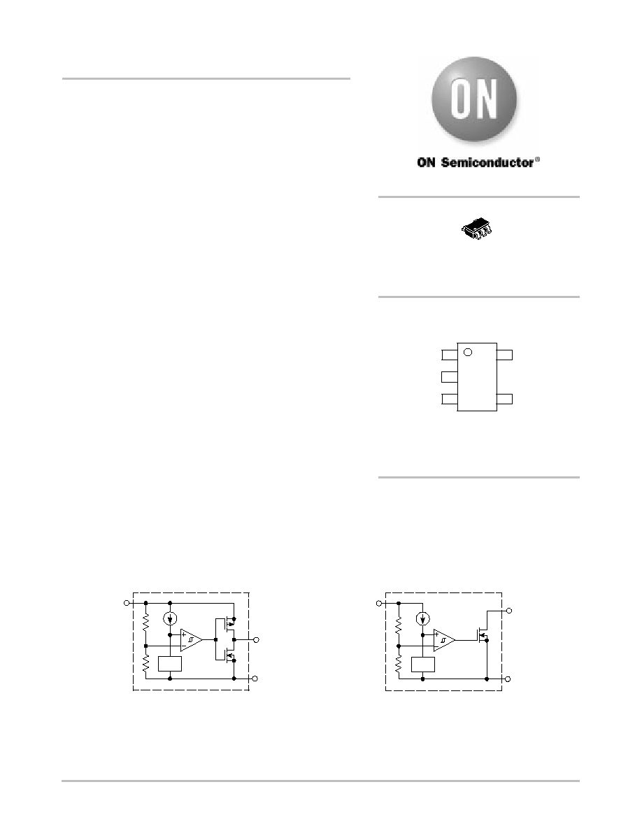
Figure 1. Representative Block Diagrams
This device contains 25 active transistors.
NCP301xSNxxT1
Open Drain Output Configuration
NCP300xSNxxT1
Complementary Output Configuration
V
ref
V
ref
Input
Reset Output
GND
3
1
2
Input
Reset Output
GND
3
1
2
*
*
* The representative block diagrams depict active low reset output `L' suffix devices. The comparator
inputs are interchanged for the active high output `H' suffix devices.
See detailed ordering and shipping information in the ordering
information section on page 20 of this data sheet.
ORDERING INFORMATION
THIN SOT23-5/TSOP-5/SC59-5
SN SUFFIX
CASE 483
PIN CONNECTIONS AND
MARKING DIAGRAM
1
3
N.C.
Reset
Output
2
Input
GND
4
N.C.
5
xxxYW
(Top View)
xxx = Specific Device Code
Y
= Year
W
= Work Week
1
5
http://onsemi.com

NCP300, NCP301
http://onsemi.com
2
MAXIMUM RATINGS
Rating
Symbol
Value
Unit
¡¡¡¡¡¡¡¡¡¡¡¡¡¡¡¡¡¡
¡¡¡¡¡¡¡¡¡¡¡¡¡¡¡¡¡¡
Input Power Supply Voltage (Pin 2)
¡¡¡¡¡¡
¡¡¡¡¡¡
V
in
¡¡¡¡¡¡¡¡
¡¡¡¡¡¡¡¡
12
¡¡¡¡
¡¡¡¡
V
¡¡¡¡¡¡¡¡¡¡¡¡¡¡¡¡¡¡
¡
¡¡¡¡¡¡¡¡¡¡¡¡¡¡¡¡
¡
¡¡¡¡¡¡¡¡¡¡¡¡¡¡¡¡¡¡
Output Voltage (Pin 1)
Complementary, NCP300
N-Channel Open Drain, NCP301
¡¡¡¡¡¡
¡
¡¡¡¡
¡
¡¡¡¡¡¡
V
OUT
¡¡¡¡¡¡¡¡
¡
¡¡¡¡¡¡
¡
¡¡¡¡¡¡¡¡
-0.3 to V
in
+0.3
-0.3 to 12
¡¡¡¡
¡
¡¡
¡
¡¡¡¡
V
¡¡¡¡¡¡¡¡¡¡¡¡¡¡¡¡¡¡
¡¡¡¡¡¡¡¡¡¡¡¡¡¡¡¡¡¡
Output Current (Pin 1) (Note 2)
¡¡¡¡¡¡
¡¡¡¡¡¡
I
OUT
¡¡¡¡¡¡¡¡
¡¡¡¡¡¡¡¡
70
¡¡¡¡
¡¡¡¡
mA
¡¡¡¡¡¡¡¡¡¡¡¡¡¡¡¡¡¡
¡¡¡¡¡¡¡¡¡¡¡¡¡¡¡¡¡¡
Thermal Resistance Junction-to-Air
¡¡¡¡¡¡
¡¡¡¡¡¡
R
q
JA
¡¡¡¡¡¡¡¡
¡¡¡¡¡¡¡¡
250
¡¡¡¡
¡¡¡¡
∞
C/W
¡¡¡¡¡¡¡¡¡¡¡¡¡¡¡¡¡¡
¡¡¡¡¡¡¡¡¡¡¡¡¡¡¡¡¡¡
Operating Junction Temperature Range
¡¡¡¡¡¡
¡¡¡¡¡¡
T
J
¡¡¡¡¡¡¡¡
¡¡¡¡¡¡¡¡
-40 to +125
¡¡¡¡
¡¡¡¡
∞
C
¡¡¡¡¡¡¡¡¡¡¡¡¡¡¡¡¡¡
¡¡¡¡¡¡¡¡¡¡¡¡¡¡¡¡¡¡
Operating Ambient Temperature Range
¡¡¡¡¡¡
¡¡¡¡¡¡
T
A
¡¡¡¡¡¡¡¡
¡¡¡¡¡¡¡¡
-40 to +85
¡¡¡¡
¡¡¡¡
∞
C
¡¡¡¡¡¡¡¡¡¡¡¡¡¡¡¡¡¡
¡¡¡¡¡¡¡¡¡¡¡¡¡¡¡¡¡¡
Storage Temperature Range
¡¡¡¡¡¡
¡¡¡¡¡¡
T
stg
¡¡¡¡¡¡¡¡
¡¡¡¡¡¡¡¡
-55 to +150
¡¡¡¡
¡¡¡¡
∞
C
¡¡¡¡¡¡¡¡¡¡¡¡¡¡¡¡¡¡
¡¡¡¡¡¡¡¡¡¡¡¡¡¡¡¡¡¡
Moisture Sensitivity Level (T
A
= 235
∞
C)
¡¡¡¡¡¡
¡¡¡¡¡¡
MSL
¡¡¡¡¡¡¡¡
¡¡¡¡¡¡¡¡
1
¡¡¡¡
¡¡¡¡
¡¡¡¡¡¡¡¡¡¡¡¡¡¡¡¡¡¡
¡
¡¡¡¡¡¡¡¡¡¡¡¡¡¡¡¡
¡
¡¡¡¡¡¡¡¡¡¡¡¡¡¡¡¡¡¡
Latchup Performance
Positive
Negative
¡¡¡¡¡¡
¡
¡¡¡¡
¡
¡¡¡¡¡¡
I
LATCHUP
¡¡¡¡¡¡¡¡
¡
¡¡¡¡¡¡
¡
¡¡¡¡¡¡¡¡
200
200
¡¡¡¡
¡
¡¡
¡
¡¡¡¡
mA
Maximum ratings are those values beyond which device damage can occur. Maximum ratings applied to the device are individual stress limit
values (not normal operating conditions) and are not valid simultaneously. If these limits are exceeded, device functional operation is not implied,
damage may occur and reliability may be affected.
1. This device series contains ESD protection and exceeds the following tests:
Human Body Model 2000 V per MIL-STD-883, Method 3015.
Machine Model Method 200 V.
2. The maximum package power dissipation limit must not be exceeded.
P
D
+
T
J(max)
*
T
A
R
q
JA

NCP300, NCP301
http://onsemi.com
3
ELECTRICAL CHARACTERISTICS
(For all values T
A
= 25
∞
C, unless otherwise noted.)
Characteristic
Symbol
Min
Typ
Max
Unit
NCP300/1 - 0.9
¡¡¡¡¡¡¡¡¡¡¡¡¡¡¡¡¡¡
¡¡¡¡¡¡¡¡¡¡¡¡¡¡¡¡¡¡
Detector Threshold (Pin 2, V
in
Decreasing)
¡¡¡¡¡
¡¡¡¡¡
V
DET-
¡¡¡¡
¡¡¡¡
0.882
¡¡¡¡
¡¡¡¡
0.900
¡¡¡¡
¡¡¡¡
0.918
¡¡¡
¡¡¡
V
Detector Threshold Hysteresis (Pin 2, V
in
Increasing)
V
HYS
0.027
0.045
0.063
V
¡¡¡¡¡¡¡¡¡¡¡¡¡¡¡¡¡¡
¡
¡¡¡¡¡¡¡¡¡¡¡¡¡¡¡¡
¡
¡¡¡¡¡¡¡¡¡¡¡¡¡¡¡¡¡¡
Supply Current (Pin 2)
(V
in
= 0.8 V)
(V
in
= 2.9 V)
¡¡¡¡¡
¡
¡¡¡
¡
¡¡¡¡¡
I
in
¡¡¡¡
¡
¡¡
¡
¡¡¡¡
-
-
¡¡¡¡
¡
¡¡
¡
¡¡¡¡
0.20
0.45
¡¡¡¡
¡
¡¡
¡
¡¡¡¡
0.6
1.2
¡¡¡
¡
¡
¡
¡¡¡
m
A
Maximum Operating Voltage (Pin 2)
V
in(max)
-
-
10
V
Minimum Operating Voltage (Pin 2)
(T
A
= -40
∞
C to 85
∞
C)
V
in(min)
-
-
0.55
0.65
0.70
0.80
V
¡¡¡¡¡¡¡¡¡¡¡¡¡¡¡¡¡¡
¡¡¡¡¡¡¡¡¡¡¡¡¡¡¡¡¡¡
Reset Output Current (Pin 1, Active Low `L' Suffix Devices)
¡¡¡¡¡
¡¡¡¡¡
I
OUT
¡¡¡¡
¡¡¡¡
¡¡¡¡
¡¡¡¡
¡¡¡¡
¡¡¡¡
¡¡¡
¡¡¡
mA
N-Channel Sink Current, NCP300, NCP301
(V
OUT
= 0.05 V, V
in
= 0.70 V)
(V
OUT
= 0.50 V, V
in
= 0.85 V)
0.01
0.05
0.05
0.50
-
-
P-Channel Source Current, NCP300
(V
OUT
= 2.4 V, V
in
= 4.5 V)
1.0
6.0
-
¡¡¡¡¡¡¡¡¡¡¡¡¡¡¡¡¡¡
¡¡¡¡¡¡¡¡¡¡¡¡¡¡¡¡¡¡
Reset Output Current (Pin 1, Active High `H' Suffix Devices)
¡¡¡¡¡
¡¡¡¡¡
I
OUT
¡¡¡¡
¡¡¡¡
¡¡¡¡
¡¡¡¡
¡¡¡¡
¡¡¡¡
¡¡¡
¡¡¡
mA
N-Channel Sink Current, NCP300, NCP301
(V
OUT
= 0.5 V, V
in
= 1.5 V)
1.05
2.5
-
P-Channel Source Current, NCP300
(V
OUT
= 0.4 V, V
in
= 0.7 V)
(V
OUT
= GND, V
in
= 0.8 V)
0.011
0.014
0.04
0.08
-
-
¡¡¡¡¡¡¡¡¡¡¡¡¡¡¡¡¡¡
¡¡¡¡¡¡¡¡¡¡¡¡¡¡¡¡¡¡
Propagation Delay Input to Output (Figure 2)
¡¡¡¡¡
¡¡¡¡¡
¡¡¡¡
¡¡¡¡
¡¡¡¡
¡¡¡¡
¡¡¡¡
¡¡¡¡
¡¡¡
¡¡¡
m
s
Complementary Output NCP300 Series
Output Transition, High to Low
Output Transition, Low to High
t
pHL
t
pLH
-
-
97
77
-
300
N-Channel Open Drain NCP301 Series
Output Transition, High to Low
Output Transition, Low to High
t
pHL
t
pLH
-
-
97
-
-
300
NCP300/1 - 1.8
¡¡¡¡¡¡¡¡¡¡¡¡¡¡¡¡¡¡
¡¡¡¡¡¡¡¡¡¡¡¡¡¡¡¡¡¡
Detector Threshold (Pin 2, V
in
Decreasing)
¡¡¡¡¡
¡¡¡¡¡
V
DET-
¡¡¡¡
¡¡¡¡
1.764
¡¡¡¡
¡¡¡¡
1.80
¡¡¡¡
¡¡¡¡
1.836
¡¡¡
¡¡¡
V
Detector Threshold Hysteresis (Pin 2, V
in
Increasing)
V
HYS
0.054
0.090
0.126
V
¡¡¡¡¡¡¡¡¡¡¡¡¡¡¡¡¡¡
¡
¡¡¡¡¡¡¡¡¡¡¡¡¡¡¡¡
¡
¡¡¡¡¡¡¡¡¡¡¡¡¡¡¡¡¡¡
Supply Current (Pin 2)
(V
in
= 1.7 V)
(V
in
= 3.8 V)
¡¡¡¡¡
¡
¡¡¡
¡
¡¡¡¡¡
I
in
¡¡¡¡
¡
¡¡
¡
¡¡¡¡
-
-
¡¡¡¡
¡
¡¡
¡
¡¡¡¡
0.23
0.48
¡¡¡¡
¡
¡¡
¡
¡¡¡¡
0.7
1.3
¡¡¡
¡
¡
¡
¡¡¡
m
A
Maximum Operating Voltage (Pin 2)
V
in(max)
-
-
10
V
Minimum Operating Voltage (Pin 2)
(T
A
= -40
∞
C to 85
∞
C)
V
in(min)
-
-
0.55
0.65
0.70
0.80
V
¡¡¡¡¡¡¡¡¡¡¡¡¡¡¡¡¡¡
¡¡¡¡¡¡¡¡¡¡¡¡¡¡¡¡¡¡
Reset Output Current (Pin 1, Active Low `L' Suffix Devices)
¡¡¡¡¡
¡¡¡¡¡
I
OUT
¡¡¡¡
¡¡¡¡
¡¡¡¡
¡¡¡¡
¡¡¡¡
¡¡¡¡
¡¡¡
¡¡¡
mA
N-Channel Sink Current, NCP300, NCP301
(V
OUT
= 0.05V, V
in
= 0.70 V)
(V
OUT
= 0.50V, V
in
= 1.5 V)
0.01
1.0
0.05
2.0
-
-
P-Channel Source Current, NCP300
(V
OUT
= 2.4 V, V
in
= 4.5 V)
1.0
6.0
-
¡¡¡¡¡¡¡¡¡¡¡¡¡¡¡¡¡¡
¡¡¡¡¡¡¡¡¡¡¡¡¡¡¡¡¡¡
Reset Output Current (Pin 1, Active High `H' Suffix Devices)
¡¡¡¡¡
¡¡¡¡¡
I
OUT
¡¡¡¡
¡¡¡¡
¡¡¡¡
¡¡¡¡
¡¡¡¡
¡¡¡¡
¡¡¡
¡¡¡
mA
N-Channel Sink Current, NCP300, NCP301
(V
OUT
= 0.5 V, V
in
= 5.0 V)
6.3
11
-
P-Channel Source Current, NCP300
(V
OUT
= 0.4 V, V
in
= 0.7 V)
(V
OUT
= GND, V
in
= 1.5 V)
0.011
0.525
0.04
0.6
-
-
¡¡¡¡¡¡¡¡¡¡¡¡¡¡¡¡¡¡
¡¡¡¡¡¡¡¡¡¡¡¡¡¡¡¡¡¡
Propagation Delay Input to Output (Figure 2)
¡¡¡¡¡
¡¡¡¡¡
¡¡¡¡
¡¡¡¡
¡¡¡¡
¡¡¡¡
¡¡¡¡
¡¡¡¡
¡¡¡
¡¡¡
m
s

NCP300, NCP301
http://onsemi.com
4
ELECTRICAL CHARACTERISTICS
(continued) (For all values T
A
= 25
∞
C, unless otherwise noted.)
Characteristic
Unit
Max
Typ
Min
Symbol
NCP300/1 - 1.8
Complementary Output NCP300 Series
Output Transition, High to Low
Output Transition, Low to High
t
pHL
t
pLH
-
-
73
94
-
300
N-Channel Open Drain NCP301 Series
Output Transition, High to Low
Output Transition, Low to High
t
pHL
t
pLH
-
-
73
-
-
300
NCP300/1 - 2.0
¡¡¡¡¡¡¡¡¡¡¡¡¡¡¡¡¡¡
¡¡¡¡¡¡¡¡¡¡¡¡¡¡¡¡¡¡
Detector Threshold (Pin 2, V
in
Decreasing)
¡¡¡¡¡
¡¡¡¡¡
V
DET-
¡¡¡¡
¡¡¡¡
1.960
¡¡¡¡
¡¡¡¡
2.00
¡¡¡¡
¡¡¡¡
2.040
¡¡¡
¡¡¡
V
Detector Threshold Hysteresis (Pin 2, V
in
Increasing)
V
HYS
0.06
0.10
0.14
V
¡¡¡¡¡¡¡¡¡¡¡¡¡¡¡¡¡¡
¡
¡¡¡¡¡¡¡¡¡¡¡¡¡¡¡¡
¡
¡¡¡¡¡¡¡¡¡¡¡¡¡¡¡¡¡¡
Supply Current (Pin 2)
(V
in
= 1.9 V)
(V
in
= 4.0 V)
¡¡¡¡¡
¡
¡¡¡
¡
¡¡¡¡¡
I
in
¡¡¡¡
¡
¡¡
¡
¡¡¡¡
-
-
¡¡¡¡
¡
¡¡
¡
¡¡¡¡
0.23
0.48
¡¡¡¡
¡
¡¡
¡
¡¡¡¡
0.8
1.3
¡¡¡
¡
¡
¡
¡¡¡
m
A
Maximum Operating Voltage (Pin 2)
V
in(max)
-
-
10
V
Minimum Operating Voltage (Pin 2)
(T
A
= -40
∞
C to 85
∞
C)
V
in(min)
-
-
0.55
0.65
0.70
0.80
V
¡¡¡¡¡¡¡¡¡¡¡¡¡¡¡¡¡¡
¡¡¡¡¡¡¡¡¡¡¡¡¡¡¡¡¡¡
Reset Output Current (Pin 1, Active Low `L' Suffix Devices)
¡¡¡¡¡
¡¡¡¡¡
I
OUT
¡¡¡¡
¡¡¡¡
¡¡¡¡
¡¡¡¡
¡¡¡¡
¡¡¡¡
¡¡¡
¡¡¡
mA
N-Channel Sink Current, NCP300, NCP301
(V
OUT
= 0.05V, V
in
= 0.70V)
(V
OUT
= 0.50V, V
in
= 1.5V)
0.01
1.0
0.05
2.0
-
-
P-Channel Source Current, NCP300
(V
OUT
= 2.4V, V
in
= 4.5V)
1.0
6.0
-
¡¡¡¡¡¡¡¡¡¡¡¡¡¡¡¡¡¡
¡¡¡¡¡¡¡¡¡¡¡¡¡¡¡¡¡¡
Reset Output Current (Pin 1, Active High `H' Suffix Devices)
¡¡¡¡¡
¡¡¡¡¡
I
OUT
¡¡¡¡
¡¡¡¡
¡¡¡¡
¡¡¡¡
¡¡¡¡
¡¡¡¡
¡¡¡
¡¡¡
mA
N-Channel Sink Current, NCP300, NCP301
(V
OUT
= 0.5 V, V
in
= 5.0 V)
6.3
11
-
P-Channel Source Current, NCP300
(V
OUT
= 0.4 V, V
in
= 0.7 V)
(V
OUT
= GND, V
in
= 1.5 V)
0.011
0.525
0.04
0.6
-
-
¡¡¡¡¡¡¡¡¡¡¡¡¡¡¡¡¡¡
¡¡¡¡¡¡¡¡¡¡¡¡¡¡¡¡¡¡
Propagation Delay Input to Output (Figure 2)
¡¡¡¡¡
¡¡¡¡¡
¡¡¡¡
¡¡¡¡
¡¡¡¡
¡¡¡¡
¡¡¡¡
¡¡¡¡
¡¡¡
¡¡¡
m
s
Complementary Output NCP300 Series
Output Transition, High to Low
Output Transition, Low to High
t
pHL
t
pLH
-
-
55
108
-
300
N-Channel Open Drain NCP301 Series
Output Transition, High to Low
Output Transition, Low to High
t
pHL
t
pLH
-
-
55
-
-
300
NCP300/1- 2.7
¡¡¡¡¡¡¡¡¡¡¡¡¡¡¡¡¡¡
¡¡¡¡¡¡¡¡¡¡¡¡¡¡¡¡¡¡
Detector Threshold (Pin 2, V
in
Decreasing)
¡¡¡¡¡
¡¡¡¡¡
V
DET-
¡¡¡¡
¡¡¡¡
2.646
¡¡¡¡
¡¡¡¡
2.700
¡¡¡¡
¡¡¡¡
2.754
¡¡¡
¡¡¡
V
Detector Threshold Hysteresis (Pin 2, V
in
Increasing)
V
HYS
0.081
0.135
0.189
V
¡¡¡¡¡¡¡¡¡¡¡¡¡¡¡¡¡¡
¡
¡¡¡¡¡¡¡¡¡¡¡¡¡¡¡¡
¡
¡¡¡¡¡¡¡¡¡¡¡¡¡¡¡¡¡¡
Supply Current (Pin 2)
(V
in
= 2.6 V)
(V
in
= 4.7 V)
¡¡¡¡¡
¡
¡¡¡
¡
¡¡¡¡¡
I
in
¡¡¡¡
¡
¡¡
¡
¡¡¡¡
-
-
¡¡¡¡
¡
¡¡
¡
¡¡¡¡
0.26
0.46
¡¡¡¡
¡
¡¡
¡
¡¡¡¡
0.8
1.3
¡¡¡
¡
¡
¡
¡¡¡
m
A
Maximum Operating Voltage (Pin 2)
V
in(max)
-
-
10
V
Minimum Operating Voltage (Pin 2)
(T
A
= -40
∞
C to 85
∞
C)
V
in(min)
-
-
0.55
0.65
0.70
0.80
V
¡¡¡¡¡¡¡¡¡¡¡¡¡¡¡¡¡¡
¡¡¡¡¡¡¡¡¡¡¡¡¡¡¡¡¡¡
Reset Output Current (Pin 1, Active Low `L' Suffix Devices)
¡¡¡¡¡
¡¡¡¡¡
I
OUT
¡¡¡¡
¡¡¡¡
¡¡¡¡
¡¡¡¡
¡¡¡¡
¡¡¡¡
¡¡¡
¡¡¡
mA
N-Channel Sink Current, NCP300, NCP301
(V
OUT
= 0.05V, V
in
= 0.70V)
(V
OUT
= 0.50V, V
in
= 1.5V)
0.01
1.0
0.05
2.0
-
-
P-Channel Source Current, NCP300
(V
OUT
= 2.4V, V
in
= 4.5V)
1.0
6.0
-

NCP300, NCP301
http://onsemi.com
5
ELECTRICAL CHARACTERISTICS
(continued) (For all values T
A
= 25
∞
C, unless otherwise noted.)
Characteristic
Unit
Max
Typ
Min
Symbol
NCP300/1- 2.7
¡¡¡¡¡¡¡¡¡¡¡¡¡¡¡¡¡¡
¡¡¡¡¡¡¡¡¡¡¡¡¡¡¡¡¡¡
Reset Output Current (Pin 1, Active High `H' Suffix Devices)
¡¡¡¡¡
¡¡¡¡¡
I
OUT
¡¡¡¡
¡¡¡¡
¡¡¡¡
¡¡¡¡
¡¡¡¡
¡¡¡¡
¡¡¡
¡¡¡
mA
N-Channel Sink Current, NCP300, NCP301
(V
OUT
= 0.5 V, V
in
= 5.0 V)
6.3
11
-
P-Channel Source Current, NCP300
(V
OUT
= 0.4 V, V
in
= 0.7 V)
(V
OUT
= GND, V
in
= 1.5 V)
0.011
0.525
0.04
0.6
-
-
¡¡¡¡¡¡¡¡¡¡¡¡¡¡¡¡¡¡
¡¡¡¡¡¡¡¡¡¡¡¡¡¡¡¡¡¡
Propagation Delay Input to Output (Figure 2)
¡¡¡¡¡
¡¡¡¡¡
¡¡¡¡
¡¡¡¡
¡¡¡¡
¡¡¡¡
¡¡¡¡
¡¡¡¡
¡¡¡
¡¡¡
m
s
Complementary Output NCP300 Series
Output Transition, High to Low
Output Transition, Low to High
t
pHL
t
pLH
-
-
55
115
-
300
N-Channel Open Drain NCP301 Series
Output Transition, High to Low
Output Transition, Low to High
t
pHL
t
pLH
-
-
55
-
-
300
NCP300/1 - 3.0
¡¡¡¡¡¡¡¡¡¡¡¡¡¡¡¡¡¡
¡¡¡¡¡¡¡¡¡¡¡¡¡¡¡¡¡¡
Detector Threshold (Pin 2, V
in
Decreasing)
¡¡¡¡¡
¡¡¡¡¡
V
DET-
¡¡¡¡
¡¡¡¡
2.94
¡¡¡¡
¡¡¡¡
3.00
¡¡¡¡
¡¡¡¡
3.06
¡¡¡
¡¡¡
V
Detector Threshold Hysteresis (Pin 2, V
in
Increasing)
V
HYS
0.09
0.15
0.21
V
¡¡¡¡¡¡¡¡¡¡¡¡¡¡¡¡¡¡
¡
¡¡¡¡¡¡¡¡¡¡¡¡¡¡¡¡
¡
¡
¡¡¡¡¡¡¡¡¡¡¡¡¡¡¡¡
¡
¡¡¡¡¡¡¡¡¡¡¡¡¡¡¡¡¡¡
Supply Current (Pin 2)
(V
in
= 2.87 V)
(V
in
= 5.0 V)
¡¡¡¡¡
¡
¡¡¡
¡
¡
¡¡¡
¡
¡¡¡¡¡
I
in
¡¡¡¡
¡
¡¡
¡
¡
¡¡
¡
¡¡¡¡
-
-
¡¡¡¡
¡
¡¡
¡
¡
¡¡
¡
¡¡¡¡
0.27
0.47
¡¡¡¡
¡
¡¡
¡
¡
¡¡
¡
¡¡¡¡
0.9
1.3
¡¡¡
¡
¡
¡
¡
¡
¡
¡¡¡
m
A
Maximum Operating Voltage (Pin 2)
V
in(max)
-
-
10
V
Minimum Operating Voltage (Pin 2)
(T
A
= -40
∞
C to 85
∞
C)
V
in(min)
-
-
0.55
0.65
0.70
0.80
V
¡¡¡¡¡¡¡¡¡¡¡¡¡¡¡¡¡¡
¡¡¡¡¡¡¡¡¡¡¡¡¡¡¡¡¡¡
Reset Output Current (Pin 1, Active Low `L' Suffix Devices)
¡¡¡¡¡
¡¡¡¡¡
I
OUT
¡¡¡¡
¡¡¡¡
¡¡¡¡
¡¡¡¡
¡¡¡¡
¡¡¡¡
¡¡¡
¡¡¡
mA
N-Channel Sink Current, NCP300, NCP301
(V
OUT
= 0.05V, V
in
= 0.70V)
(V
OUT
= 0.50V, V
in
= 1.5V)
0.01
1.0
0.05
2.0
-
-
P-Channel Source Current, NCP300
(V
OUT
= 2.4V, V
in
= 4.5V)
1.0
6.0
-
¡¡¡¡¡¡¡¡¡¡¡¡¡¡¡¡¡¡
¡¡¡¡¡¡¡¡¡¡¡¡¡¡¡¡¡¡
Reset Output Current (Pin 1, Active High `H' Suffix Devices)
¡¡¡¡¡
¡¡¡¡¡
I
OUT
¡¡¡¡
¡¡¡¡
¡¡¡¡
¡¡¡¡
¡¡¡¡
¡¡¡¡
¡¡¡
¡¡¡
mA
N-Channel Sink Current, NCP300, NCP301
(V
OUT
= 0.5 V, V
in
= 5.0 V)
6.3
11
-
P-Channel Source Current, NCP300
(V
OUT
= 0.4 V, V
in
= 0.7 V)
(V
OUT
= GND, V
in
= 1.5 V)
0.011
0.525
0.04
0.6
-
-
¡¡¡¡¡¡¡¡¡¡¡¡¡¡¡¡¡¡
¡¡¡¡¡¡¡¡¡¡¡¡¡¡¡¡¡¡
Propagation Delay Input to Output (Figure 2)
¡¡¡¡¡
¡¡¡¡¡
¡¡¡¡
¡¡¡¡
¡¡¡¡
¡¡¡¡
¡¡¡¡
¡¡¡¡
¡¡¡
¡¡¡
m
s
Complementary Output NCP300 Series
Output Transition, High to Low
Output Transition, Low to High
t
pHL
t
pLH
-
-
49
115
-
300
N-Channel Open Drain NCP301 Series
Output Transition, High to Low
Output Transition, Low to High
t
pHL
t
pLH
-
-
49
-
-
300
NCP300/1 - 4.5
¡¡¡¡¡¡¡¡¡¡¡¡¡¡¡¡¡¡
Detector Threshold (Pin 2, V
in
Decreasing)
¡¡¡¡¡
V
DET-
¡¡¡¡
4.410
¡¡¡¡
4.500
¡¡¡¡
4.590
¡¡¡
V
Detector Threshold Hysteresis (Pin 2, V
in
Increasing)
V
HYS
0.135
0.225
0.315
V
¡¡¡¡¡¡¡¡¡¡¡¡¡¡¡¡¡¡
¡
¡¡¡¡¡¡¡¡¡¡¡¡¡¡¡¡
¡
¡
¡¡¡¡¡¡¡¡¡¡¡¡¡¡¡¡
¡
¡¡¡¡¡¡¡¡¡¡¡¡¡¡¡¡¡¡
Supply Current (Pin 2)
(V
in
= 4.34 V)
(V
in
= 6.5 V)
¡¡¡¡¡
¡
¡¡¡
¡
¡
¡¡¡
¡
¡¡¡¡¡
I
in
¡¡¡¡
¡
¡¡
¡
¡
¡¡
¡
¡¡¡¡
-
-
¡¡¡¡
¡
¡¡
¡
¡
¡¡
¡
¡¡¡¡
0.33
0.52
¡¡¡¡
¡
¡¡
¡
¡
¡¡
¡
¡¡¡¡
1.0
1.4
¡¡¡
¡
¡
¡
¡
¡
¡
¡¡¡
m
A
Maximum Operating Voltage (Pin 2)
V
in(max)
-
-
10
V

NCP300, NCP301
http://onsemi.com
6
ELECTRICAL CHARACTERISTICS
(continued) (For all values T
A
= 25
∞
C, unless otherwise noted.)
Characteristic
Unit
Max
Typ
Min
Symbol
NCP300/1 - 4.5
Minimum Operating Voltage (Pin 2)
(T
A
= -40
∞
C to 85
∞
C)
V
in(min)
-
-
0.55
0.65
0.70
0.80
V
¡¡¡¡¡¡¡¡¡¡¡¡¡¡¡¡¡¡
¡¡¡¡¡¡¡¡¡¡¡¡¡¡¡¡¡¡
Reset Output Current (Pin 1, Active Low `L' Suffix Devices)
¡¡¡¡¡
¡¡¡¡¡
I
OUT
¡¡¡¡
¡¡¡¡
¡¡¡¡
¡¡¡¡
¡¡¡¡
¡¡¡¡
¡¡¡
¡¡¡
mA
N-Channel Sink Current, NCP300, NCP301
(V
OUT
= 0.05V, V
in
= 0.70V)
(V
OUT
= 0.50V, V
in
= 1.5V)
0.01
1.0
0.05
2.0
-
-
P-Channel Source Current, NCP300
(V
OUT
= 5.9V, V
in
= 8.0V)
1.5
10.5
-
¡¡¡¡¡¡¡¡¡¡¡¡¡¡¡¡¡¡
¡¡¡¡¡¡¡¡¡¡¡¡¡¡¡¡¡¡
Reset Output Current (Pin 1, Active High `H' Suffix Devices)
¡¡¡¡¡
¡¡¡¡¡
I
OUT
¡¡¡¡
¡¡¡¡
¡¡¡¡
¡¡¡¡
¡¡¡¡
¡¡¡¡
¡¡¡
¡¡¡
mA
N-Channel Sink Current, NCP300, NCP301
(V
OUT
= 0.5 V, V
in
= 5.0 V)
6.3
11
-
P-Channel Source Current, NCP300
(V
OUT
= 0.4 V, V
in
= 0.7 V)
(V
OUT
= GND, V
in
= 1.5 V)
0.011
0.525
0.04
0.6
-
-
¡¡¡¡¡¡¡¡¡¡¡¡¡¡¡¡¡¡
¡¡¡¡¡¡¡¡¡¡¡¡¡¡¡¡¡¡
Propagation Delay Input to Output (Figure 2)
¡¡¡¡¡
¡¡¡¡¡
¡¡¡¡
¡¡¡¡
¡¡¡¡
¡¡¡¡
¡¡¡¡
¡¡¡¡
¡¡¡
¡¡¡
m
s
Complementary Output NCP300 Series
Output Transition, High to Low
Output Transition, Low to High
t
pHL
t
pLH
-
-
49
130
-
300
N-Channel Open Drain NCP301 Series
Output Transition, High to Low
Output Transition, Low to High
t
pHL
t
pLH
-
-
49
-
-
300
NCP300/1 - 4.7
¡¡¡¡¡¡¡¡¡¡¡¡¡¡¡¡¡¡
¡¡¡¡¡¡¡¡¡¡¡¡¡¡¡¡¡¡
Detector Threshold (Pin 2, V
in
Decreasing)
¡¡¡¡¡
¡¡¡¡¡
V
DET-
¡¡¡¡
¡¡¡¡
4.606
¡¡¡¡
¡¡¡¡
4.70
¡¡¡¡
¡¡¡¡
4.794
¡¡¡
¡¡¡
V
Detector Threshold Hysteresis (Pin 2, V
in
Increasing)
V
HYS
0.141
0.235
0.329
V
¡¡¡¡¡¡¡¡¡¡¡¡¡¡¡¡¡¡
¡
¡¡¡¡¡¡¡¡¡¡¡¡¡¡¡¡
¡
¡¡¡¡¡¡¡¡¡¡¡¡¡¡¡¡¡¡
Supply Current (Pin 2)
(V
in
= 4.54 V)
(V
in
= 6.7 V)
¡¡¡¡¡
¡
¡¡¡
¡
¡¡¡¡¡
I
in
¡¡¡¡
¡
¡¡
¡
¡¡¡¡
-
-
¡¡¡¡
¡
¡¡
¡
¡¡¡¡
0.34
0.53
¡¡¡¡
¡
¡¡
¡
¡¡¡¡
1.0
1.4
¡¡¡
¡
¡
¡
¡¡¡
m
A
Maximum Operating Voltage (Pin 2)
V
in(max)
-
-
10
V
Minimum Operating Voltage (Pin 2)
(T
A
= -40
∞
C to 85
∞
C)
V
in(min)
-
-
0.55
0.65
0.70
0.80
V
¡¡¡¡¡¡¡¡¡¡¡¡¡¡¡¡¡¡
¡¡¡¡¡¡¡¡¡¡¡¡¡¡¡¡¡¡
Reset Output Current (Pin 1, Active Low `L' Suffix Devices)
¡¡¡¡¡
¡¡¡¡¡
I
OUT
¡¡¡¡
¡¡¡¡
¡¡¡¡
¡¡¡¡
¡¡¡¡
¡¡¡¡
¡¡¡
¡¡¡
mA
N-Channel Sink Current, NCP300, NCP301
(V
OUT
= 0.05V, V
in
= 0.70V)
(V
OUT
= 0.50V, V
in
= 1.5V)
0.01
1.0
0.05
2.0
-
-
P-Channel Source Current, NCP300
(V
OUT
= 5.9V, V
in
= 8.0V)
1.5
10.5
-
¡¡¡¡¡¡¡¡¡¡¡¡¡¡¡¡¡¡
¡¡¡¡¡¡¡¡¡¡¡¡¡¡¡¡¡¡
Reset Output Current (Pin 1, Active High `H' Suffix Devices)
¡¡¡¡¡
¡¡¡¡¡
I
OUT
¡¡¡¡
¡¡¡¡
¡¡¡¡
¡¡¡¡
¡¡¡¡
¡¡¡¡
¡¡¡
¡¡¡
mA
N-Channel Sink Current, NCP300, NCP301
(V
OUT
= 0.5 V, V
in
= 5.0 V)
6.3
11
-
P-Channel Source Current, NCP300
(V
OUT
= 0.4 V, V
in
= 0.7 V)
(V
OUT
= GND, V
in
= 1.5 V)
0.011
0.525
0.04
0.6
-
-
¡¡¡¡¡¡¡¡¡¡¡¡¡¡¡¡¡¡
¡¡¡¡¡¡¡¡¡¡¡¡¡¡¡¡¡¡
Propagation Delay Input to Output (Figure 2)
¡¡¡¡¡
¡¡¡¡¡
¡¡¡¡
¡¡¡¡
¡¡¡¡
¡¡¡¡
¡¡¡¡
¡¡¡¡
¡¡¡
¡¡¡
m
s
Complementary Output NCP300 Series
Output Transition, High to Low
Output Transition, Low to High
t
pHL
t
pLH
-
-
45
130
-
300
N-Channel Open Drain NCP301 Series
Output Transition, High to Low
Output Transition, Low to High
t
pHL
t
pLH
-
-
45
-
-
300
NCP300, NCP301
http://onsemi.com
7
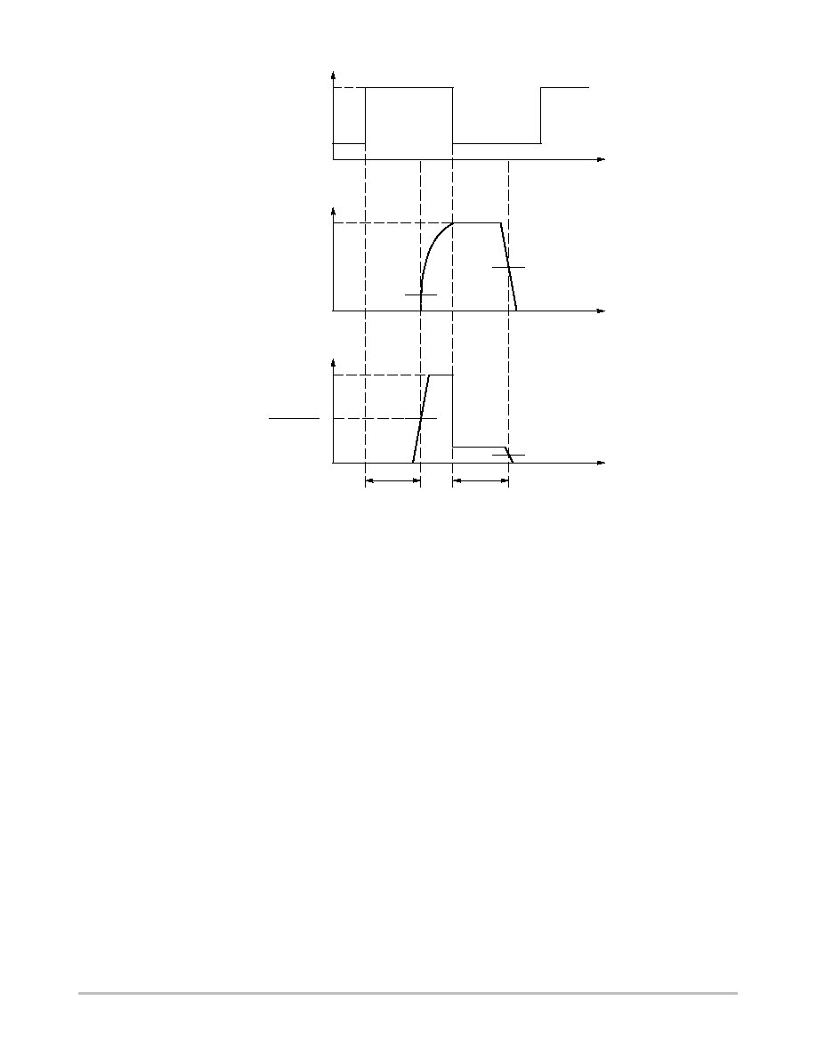
Input Voltage, Pin 2
Reset Output Voltage, Pin 1
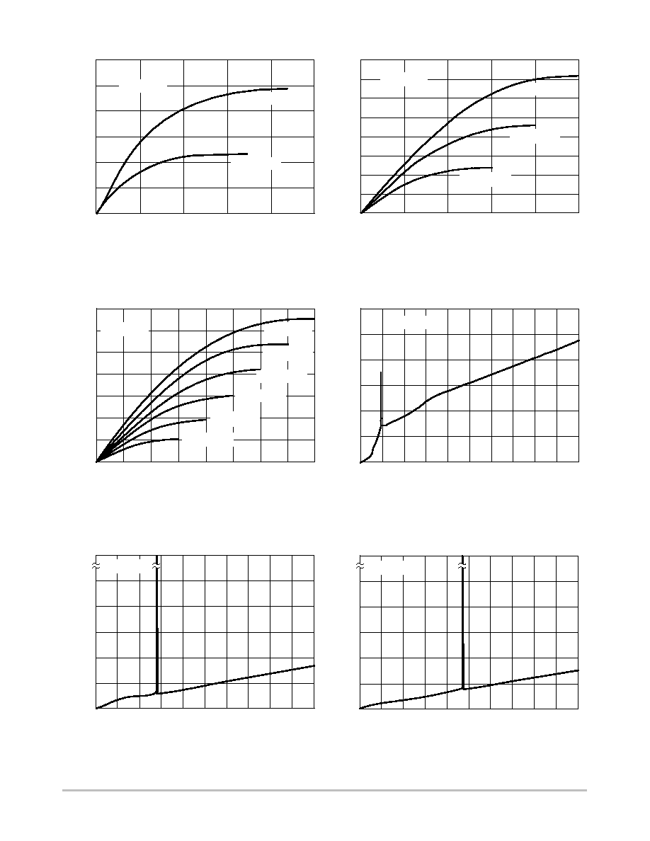
Figure 2. Propagation Delay Measurement Conditions
0.7
0 V
5 V
0 V
0.5 V
2.5 V
NCP300L
Complementary
NCP301L
Open Drain
t
pLH
t
pHL
0.1 V
Reset Output Voltage, Pin 1
0 V
V
DET+
+ 2
V
DET+
+ 2
V
DET+
+ 2
2
NCP300 and NCP301 series are measured with a 10 pF capacitive load. NCP301 has an additional 470 k pull-up resistor con-
nected from the reset output to +5.0 V. The reset output voltage waveforms are shown for the active low `L' devices. The upper
detector threshold, V
DET+
is the sum of the lower detector threshold, V
DET-
plus the input hysteresis, V
HYS
.
NCP300, NCP301
http://onsemi.com
8
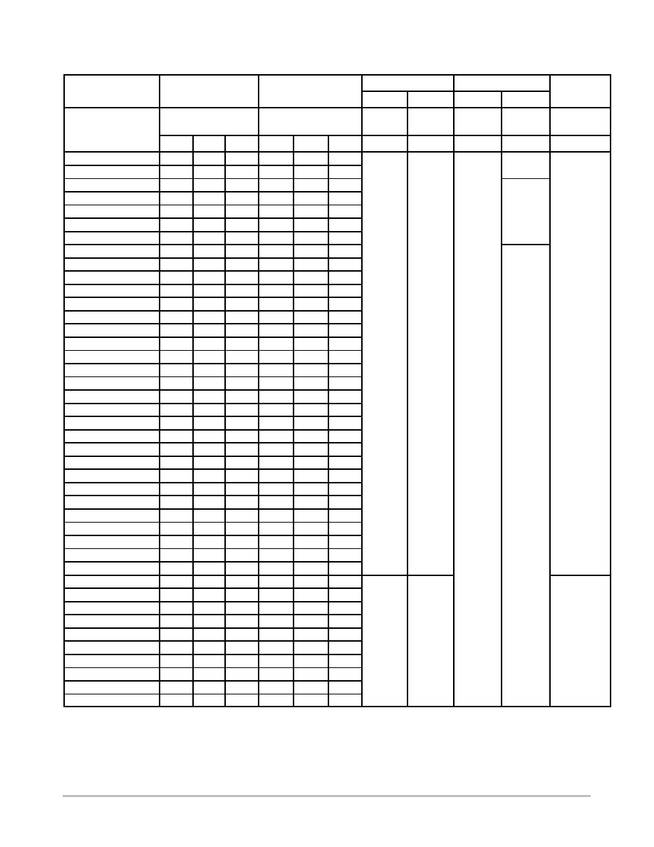
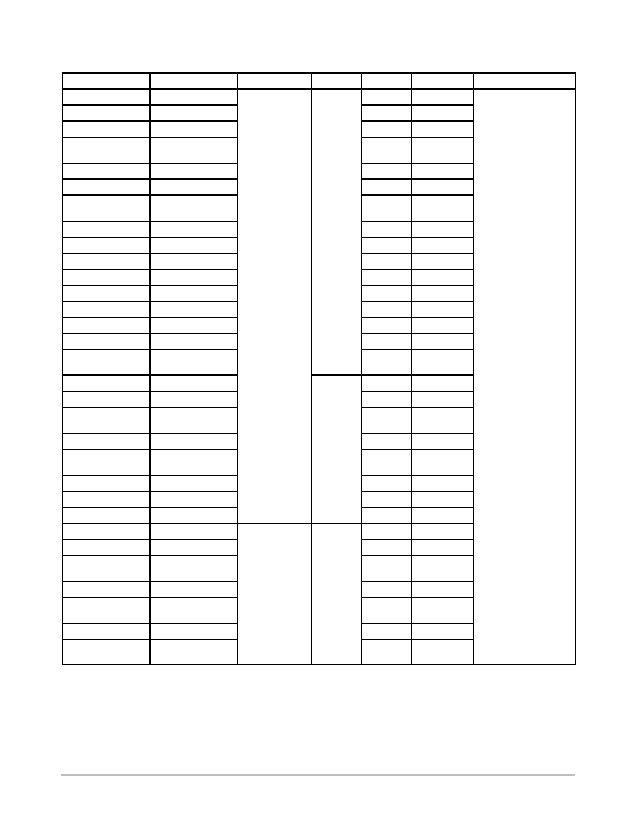
Table 1. ELECTRICAL CHARACTERISTIC TABLE FOR 0.9 - 4.9 V
Detector Threshold
Supply Current
Nch Sink Current
Pch Source
NCP300 Series
Detector Threshold
Detector Threshold
Hysteresis
V
in
Low
V
in
High
V
in
Low
V
in
High
Pch
Source
Current
V
DET-
(V)
V
HYS
(V)
I
in
(
m
A)
(Note 3)
I
in
(
m
A)
(Note 4)
I
OUT
(mA)
(Note 5)
I
OUT
(mA)
(Note 6)
I
OUT
(mA)
(Note 7)
Part Number
Min
Typ
Max
Min
Typ
Max
Typ
Typ
Typ
Typ
Typ
NCP300LSN09T1
0.882
0.9
0.918
0.027
0.045
0.063
0.3
0.5
0.05
0.5
2.0
NCP300LSN10T1
0.980
1.0
1.020
0.030
0.050
0.070
NCP300LSN11T1
1.078
1.1
1.122
0.033
0.055
0.077
1.0
NCP300LSN12T1
1.176
1.2
1.224
0.036
0.060
0.084
NCP300LSN13T1
1.274
1.3
1.326
0.039
0.065
0.091
NCP300LSN14T1
1.372
1.4
1.428
0.042
0.070
0.098
NCP300LSN15T1
1.470
1.5
1.530
0.045
0.075
0.105
NCP300LSN16T1
1.568
1.6
1.632
0.048
0.080
0.112
2.0
NCP300LSN17T1
1.666
1.7
1.734
0.051
0.085
0.119
NCP300LSN18T1
1.764
1.8
1.836
0.054
0.090
0.126
NCP300LSN185T1
1.813
1.85
1.887
0.056
0.093
0.130
NCP300LSN19T1
1.862
1.9
1.938
0.057
0.095
0.133
NCP300LSN20T1
1.960
2.0
2.040
0.060
0.100
0.140
NCP300LSN21T1
2.058
2.1
2.142
0.063
0.105
0.147
NCP300LSN22T1
2.156
2.2
2.244
0.066
0.110
0.154
NCP300LSN23T1
2.254
2.3
2.346
0.069
0.115
0.161
NCP300LSN24T1
2.352
2.4
2.448
0.072
0.120
0.168
NCP300LSN25T1
2.450
2.5
2.550
0.075
0.125
0.175
NCP300LSN26T1
2.548
2.6
2.652
0.078
0.130
0.182
NCP300LSN27T1
2.646
2.7
2.754
0.081
0.135
0.189
NCP300LSN28T1
2.744
2.8
2.856
0.084
0.140
0.196
NCP300LSN29T1
2.842
2.9
2.958
0.087
0.145
0.203
NCP300LSN30T1
2.940
3.0
3.060
0.090
0.150
0.210
NCP300LSN31T1
3.038
3.1
3.162
0.093
0.155
0.217
NCP300LSN32T1
3.136
3.2
3.264
0.096
0.160
0.224
NCP300LSN33T1
3.234
3.3
3.366
0.099
0.165
0.231
NCP300LSN34T1
3.332
3.4
3.468
0.102
0.170
0.238
NCP300LSN35T1
3.430
3.5
3.570
0.105
0.175
0.245
NCP300LSN36T1
3.528
3.6
3.672
0.108
0.180
0.252
NCP300LSN37T1
3.626
3.7
3.774
0.111
0.185
0.259
NCP300LSN38T1
3.724
3.8
3.876
0.114
0.190
0.266
NCP300LSN39T1
3.822
3.9
3.978
0.117
0.195
0.273
NCP300LSN40T1
3.920
4.0
4.080
0.120
0.200
0.280
0.4
0.6
3.0
NCP300LSN41T1
4.018
4.1
4.182
0.123
0.205
0.287
NCP300LSN42T1
4.116
4.2
4.284
0.126
0.210
0.294
NCP300LSN43T1
4.214
4.3
4.386
0.129
0.215
0.301
NCP300LSN44T1
4.312
4.4
4.488
0.132
0.220
0.308
NCP300LSN45T1
4.410
4.5
4.590
0.135
0.225
0.315
NCP300LSN46T1
4.508
4.6
4.692
0.138
0.230
0.322
NCP300LSN47T1
4.606
4.7
4.794
0.141
0.235
0.329
NCP300LSN48T1
4.704
4.8
4.896
0.144
0.240
0.336
NCP300LSN49T1
4.802
4.9
4.998
0.147
0.245
0.343
3. Condition 1: 0.9 - 2.9 V, V
in
= V
DET-
- 0.10 V; 3.0 - 3.9 V, V
in
= V
DET-
- 0.13 V; 4.0 - 4.9 V, V
in
= V
DET-
- 0.16 V
4. Condition 2: 0.9 - 4.9 V, V
in
= V
DET-
+ 2.0 V
5. Condition 3: 0.9 - 4.9 V, V
in
= 0.7 V, V
OUT
= 0.05 V, Active Low `L' Suffix Devices
6. Condition 4: 0.9 - 1.0 V, V
in
= 0.85 V, V
OUT
= 0.5 V; 1.1 - 1.5 V, V
in
= 1.0 V, V
OUT
= 0.5 V; 1.6 - 4.9 V, V
in
= 1.5 V, V
OUT
= 0.5 V,
Condition 4:
Active Low `L' Suffix Devices
7. Condition 5: 0.9 - 3.9 V, V
in
= 4.5 V, V
OUT
= 2.4 V; 4.0 - 4.9 V, V
in
= 8.0 V, V
OUT
= 5.9 V, Active Low `L' Suffix Devices
NCP300, NCP301
http://onsemi.com
9
Table 2. ELECTRICAL CHARACTERISTIC TABLE FOR 0.9 - 4.9 V
Detector Threshold
Supply Current
Nch Sink
Pch Source Current
NCP300 Series
Detector Threshold
Detector Threshold
Hysteresis
V
in
Low
V
in
High
Nch
Sink
Current
V
in
Low
V
in
High
V
DET-
(V)
V
HYS
(V)
I
in
(
m
A)
(Note 8)
I
in
(
m
A)
(Note 9)
I
OUT
(mA)
(Note 10)
I
OUT
(mA)
(Note 11)
I
OUT
(mA)
(Note 12)
Part Number
Min
Typ
Max
Min
Typ
Max
Typ
Typ
Typ
Typ
Typ
NCP300HSN09T1
0.882
0.9
0.918
0.027
0.045
0.063
0.3
0.5
2.5
0.04
0.08
NCP300HSN10T1
0.980
1.0
1.020
0.030
0.050
0.070
NCP300HSN11T1
1.078
1.1
1.122
0.033
0.055
0.077
0.18
NCP300HSN12T1
1.176
1.2
1.224
0.036
0.060
0.084
NCP300HSN13T1
1.274
1.3
1.326
0.039
0.065
0.091
NCP300HSN14T1
1.372
1.4
1.428
0.042
0.070
0.098
NCP300HSN15T1
1.470
1.5
1.530
0.045
0.075
0.105
11
NCP300HSN16T1
1.568
1.6
1.632
0.048
0.080
0.112
0.6
NCP300HSN17T1
1.666
1.7
1.734
0.051
0.085
0.119
NCP300HSN18T1
1.764
1.8
1.836
0.054
0.090
0.126
NCP300HSN19T1
1.862
1.9
1.938
0.057
0.095
0.133
NCP300HSN20T1
1.960
2.0
2.040
0.060
0.100
0.140
NCP300HSN21T1
2.058
2.1
2.142
0.063
0.105
0.147
NCP300HSN22T1
2.156
2.2
2.244
0.066
0.110
0.154
NCP300HSN23T1
2.254
2.3
2.346
0.069
0.115
0.161
NCP300HSN24T1
2.352
2.4
2.448
0.072
0.120
0.168
NCP300HSN25T1
2.450
2.5
2.550
0.075
0.125
0.175
NCP300HSN26T1
2.548
2.6
2.652
0.078
0.130
0.182
NCP300HSN27T1
2.646
2.7
2.754
0.081
0.135
0.189
NCP300HSN28T1
2.744
2.8
2.856
0.084
0.140
0.196
NCP300HSN29T1
2.842
2.9
2.958
0.087
0.145
0.203
NCP300HSN30T1
2.940
3.0
3.060
0.090
0.150
0.210
NCP300HSN31T1
3.038
3.1
3.162
0.093
0.155
0.217
NCP300HSN32T1
3.136
3.2
3.264
0.096
0.160
0.224
NCP300HSN33T1
3.234
3.3
3.366
0.099
0.165
0.231
NCP300HSN34T1
3.332
3.4
3.468
0.102
0.170
0.238
NCP300HSN35T1
3.430
3.5
3.570
0.105
0.175
0.245
NCP300HSN36T1
3.528
3.6
3.672
0.108
0.180
0.252
NCP300HSN37T1
3.626
3.7
3.774
0.111
0.185
0.259
NCP300HSN38T1
3.724
3.8
3.876
0.114
0.190
0.266
NCP300HSN39T1
3.822
3.9
3.978
0.117
0.195
0.273
NCP300HSN40T1
3.920
4.0
4.080
0.120
0.200
0.280
0.4
0.6
NCP300HSN41T1
4.018
4.1
4.182
0.123
0.205
0.287
NCP300HSN42T1
4.116
4.2
4.284
0.126
0.210
0.294
NCP300HSN43T1
4.214
4.3
4.386
0.129
0.215
0.301
NCP300HSN44T1
4.312
4.4
4.488
0.132
0.220
0.308
NCP300HSN45T1
4.410
4.5
4.590
0.135
0.225
0.315
NCP300HSN46T1
4.508
4.6
4.692
0.138
0.230
0.322
NCP300HSN47T1
4.606
4.7
4.794
0.141
0.235
0.329
NCP300HSN48T1
4.704
4.8
4.896
0.144
0.240
0.336
NCP300HSN49T1
4.802
4.9
4.998
0.147
0.245
0.343
8. Condition 1: 0.9 - 2.9 V, V
in
= V
DET-
- 0.10 V; 3.0 - 3.9 V, V
in
= V
DET-
- 0.13 V; 4.0 - 4.9 V, V
in
= V
DET-
- 0.16 V
9. Condition 2: 0.9 - 4.9 V, V
in
= V
DET-
+ 2.0 V
10. Condition 3: 0.9 - 1.4 V, V
in
= 1.5 V, V
OUT
= 0.5 V; 1.5 - 4.9 V, V
in
= 5.0 V, V
OUT
= 0.5 V, Active High `H' Suffix Devices
11. Condition 4: 0.9 - 4.9 V, V
in
= 0.7 V, V
OUT
= 0.4 V, Active High `H' Suffix Devices
12. Condition 5: 0.9 - 1.0 V, V
in
= 0.8 V, V
OUT
= GND; 1.1 - 1.5 V, V
in
= 1.0 V, V
OUT
= GND; 1.6 - 4.9 V, V
in
= 1.5 V, V
OUT
= GND,
Active High `H' Suffix Devices
NCP300, NCP301
http://onsemi.com
10
Table 3. ELECTRICAL CHARACTERISTIC TABLE FOR 0.9 - 4.9 V
Detector Threshold
Supply Current
Nch Sink Current
NCP301 Series
Detector Threshold
Detector Threshold
Hysteresis
V
in
Low
V
in
High
V
in
Low
V
in
High
V
DET-
(V)
V
HYS
(V)
I
in
(
m
A)
(Note 13)
I
in
(
m
A)
(Note 14)
I
OUT
(mA)
(Note 15)
I
OUT
(mA)
(Note 16)
Part Number
Min
Typ
Max
Min
Typ
Max
Typ
Typ
Typ
Typ
NCP301LSN09T1
0.882
0.9
0.918
0.027
0.045
0.063
0.3
0.5
0.05
0.5
NCP301LSN10T1
0.980
1.0
1.020
0.030
0.050
0.070
NCP301LSN11T1
1.078
1.1
1.122
0.033
0.055
0.077
1.0
NCP301LSN12T1
1.176
1.2
1.224
0.036
0.060
0.084
NCP301LSN13T1
1.274
1.3
1.326
0.039
0.065
0.091
NCP301LSN14T1
1.372
1.4
1.428
0.042
0.070
0.098
NCP301LSN15T1
1.470
1.5
1.530
0.045
0.075
0.105
NCP301LSN16T1
1.568
1.6
1.632
0.048
0.080
0.112
2.0
NCP301LSN17T1
1.666
1.7
1.734
0.051
0.085
0.119
NCP301LSN18T1
1.764
1.8
1.836
0.054
0.090
0.126
NCP301LSN19T1
1.862
1.9
1.938
0.057
0.095
0.133
NCP301LSN20T1
1.960
2.0
2.040
0.060
0.100
0.140
NCP301LSN21T1
2.058
2.1
2.142
0.063
0.105
0.147
NCP301LSN22T1
2.156
2.2
2.244
0.066
0.110
0.154
NCP301LSN23T1
2.254
2.3
2.346
0.069
0.115
0.161
NCP301LSN24T1
2.352
2.4
2.448
0.072
0.120
0.168
NCP301LSN25T1
2.450
2.5
2.550
0.075
0.125
0.175
NCP301LSN26T1
2.548
2.6
2.652
0.078
0.130
0.182
NCP301LSN27T1
2.646
2.7
2.754
0.081
0.135
0.189
NCP301LSN28T1
2.744
2.8
2.856
0.084
0.140
0.196
NCP301LSN29T1
2.842
2.9
2.958
0.087
0.145
0.203
NCP301LSN30T1
2.940
3.0
3.060
0.090
0.150
0.210
NCP301LSN31T1
3.038
3.1
3.162
0.093
0.155
0.217
NCP301LSN32T1
3.136
3.2
3.264
0.096
0.160
0.224
NCP301LSN33T1
3.234
3.3
3.366
0.099
0.165
0.231
NCP301LSN34T1
3.332
3.4
3.468
0.102
0.170
0.238
NCP301LSN35T1
3.430
3.5
3.570
0.105
0.175
0.245
NCP301LSN36T1
3.528
3.6
3.672
0.108
0.180
0.252
NCP301LSN37T1
3.626
3.7
3.774
0.111
0.185
0.259
NCP301LSN38T1
3.724
3.8
3.876
0.114
0.190
0.266
NCP301LSN39T1
3.822
3.9
3.978
0.117
0.195
0.273
NCP301LSN40T1
3.920
4.0
4.080
0.120
0.200
0.280
0.4
0.6
NCP301LSN41T1
4.018
4.1
4.182
0.123
0.205
0.287
NCP301LSN42T1
4.116
4.2
4.284
0.126
0.210
0.294
NCP301LSN43T1
4.214
4.3
4.386
0.129
0.215
0.301
NCP301LSN44T1
4.312
4.4
4.488
0.132
0.220
0.308
NCP301LSN45T1
4.410
4.5
4.590
0.135
0.225
0.315
NCP301LSN46T1
4.508
4.6
4.692
0.138
0.230
0.322
NCP301LSN47T1
4.606
4.7
4.794
0.141
0.235
0.329
NCP301LSN48T1
4.704
4.8
4.896
0.144
0.240
0.336
NCP301LSN49T1
4.802
4.9
4.998
0.147
0.245
0.343
13. Condition 1: 0.9 - 2.9 V, V
in
= V
DET-
- 0.10 V; 3.0 - 3.9 V, V
in
= V
DET-
- 0.13 V; 4.0 - 4.9 V, V
in
= V
DET-
- 0.16 V
14. Condition 2: 0.9 - 4.9 V, V
in
= V
DET-
+ 2.0 V
15. Condition 3: 0.9 - 4.9 V, V
in
= 0.7 V, V
OUT
= 0.05 V, Active Low `L' Suffix Devices
16. Condition 4: 0.9 - 1.0 V, V
in
= 0.85 V, V
OUT
= 0.5 V; 1.1 - 1.5 V, V
in
= 1.0 V, V
OUT
= 0.5 V; 1.6 - 4.9 V, V
in
= 1.5 V, V
OUT
= 0.5 V,
Condition 4:
Active Low `L' Suffix Devices
NCP300, NCP301
http://onsemi.com
11
Table 4. ELECTRICAL CHARACTERISTIC TABLE FOR 0.9 - 4.9 V
Detector Threshold
Supply Current
Nch
NCP301 Series
Detector Threshold
Detector Threshold
Hysteresis
V
in
Low
V
in
High
Nch
Sink Current
V
DET-
(V)
V
HYS
(V)
I
in
(
m
A)
(Note 17)
I
in
(
m
A)
(Note 18)
I
OUT
(mA)
(Note 19)
Part Number
Min
Typ
Max
Min
Typ
Max
Typ
Typ
Typ
NCP301HSN09T1
0.882
0.9
0.918
0.027
0.045
0.063
0.3
0.5
2.5
NCP301HSN10T1
0.980
1.0
1.020
0.030
0.050
0.070
NCP301HSN11T1
1.078
1.1
1.122
0.033
0.055
0.077
NCP301HSN12T1
1.176
1.2
1.224
0.036
0.060
0.084
NCP301HSN13T1
1.274
1.3
1.326
0.039
0.065
0.091
NCP301HSN14T1
1.372
1.4
1.428
0.042
0.070
0.098
NCP301HSN15T1
1.470
1.5
1.530
0.045
0.075
0.105
11
NCP301HSN16T1
1.568
1.6
1.632
0.048
0.080
0.112
NCP301HSN17T1
1.666
1.7
1.734
0.051
0.085
0.119
NCP301HSN18T1
1.764
1.8
1.836
0.054
0.090
0.126
NCP301HSN19T1
1.862
1.9
1.938
0.057
0.095
0.133
NCP301HSN20T1
1.960
2.0
2.040
0.060
0.100
0.140
NCP301HSN21T1
2.058
2.1
2.142
0.063
0.105
0.147
NCP301HSN22T1
2.156
2.2
2.244
0.066
0.110
0.154
NCP301HSN23T1
2.254
2.3
2.346
0.069
0.115
0.161
NCP301HSN24T1
2.352
2.4
2.448
0.072
0.120
0.168
NCP301HSN25T1
2.450
2.5
2.550
0.075
0.125
0.175
NCP301HSN26T1
2.548
2.6
2.652
0.078
0.130
0.182
NCP301HSN27T1
2.646
2.7
2.754
0.081
0.135
0.189
NCP301HSN28T1
2.744
2.8
2.856
0.084
0.140
0.196
NCP301HSN29T1
2.842
2.9
2.958
0.087
0.145
0.203
NCP301HSN30T1
2.940
3.0
3.060
0.090
0.150
0.210
NCP301HSN31T1
3.038
3.1
3.162
0.093
0.155
0.217
NCP301HSN32T1
3.136
3.2
3.264
0.096
0.160
0.224
NCP301HSN33T1
3.234
3.3
3.366
0.099
0.165
0.231
NCP301HSN34T1
3.332
3.4
3.468
0.102
0.170
0.238
NCP301HSN35T1
3.430
3.5
3.570
0.105
0.175
0.245
NCP301HSN36T1
3.528
3.6
3.672
0.108
0.180
0.252
NCP301HSN37T1
3.626
3.7
3.774
0.111
0.185
0.259
NCP301HSN38T1
3.724
3.8
3.876
0.114
0.190
0.266
NCP301HSN39T1
3.822
3.9
3.978
0.117
0.195
0.273
NCP301HSN40T1
3.920
4.0
4.080
0.120
0.200
0.280
0.4
0.6
NCP301HSN41T1
4.018
4.1
4.182
0.123
0.205
0.287
NCP301HSN42T1
4.116
4.2
4.284
0.126
0.210
0.294
NCP301HSN43T1
4.214
4.3
4.386
0.129
0.215
0.301
NCP301HSN44T1
4.312
4.4
4.488
0.132
0.220
0.308
NCP301HSN45T1
4.410
4.5
4.590
0.135
0.225
0.315
NCP301HSN46T1
4.508
4.6
4.692
0.138
0.230
0.322
NCP301HSN47T1
4.606
4.7
4.794
0.141
0.235
0.329
NCP301HSN48T1
4.704
4.8
4.896
0.144
0.240
0.336
NCP301HSN49T1
4.802
4.9
4.998
0.147
0.245
0.343
17. Condition 1: 0.9 - 2.9 V, V
in
= V
DET-
- 0.10 V; 3.0 - 3.9 V, V
in
= V
DET-
- 0.13 V; 4.0 - 4.9 V, V
in
= V
DET-
- 0.16 V
18. Condition 2: 0.9 - 4.9 V, V
in
= V
DET-
+ 2.0 V
19. Condition 3: 0.9 - 1.4 V, V
in
= 1.5 V, V
OUT
= 0.5 V; 1.5 - 4.9 V, V
in
= 5.0 V, V
OUT
= 0.5 V, Active High `H' Suffix Devices

NCP300, NCP301
http://onsemi.com
12
V
OUT
, OUTPUT VOL
T
AGE (V)
V
OUT
, OUTPUT VOL
T
AGE (V)
V
OUT
, OUTPUT VOL
T
AGE (V)
V
DET
, DETECT
OR THRESHOLD VOL
T
AGE (V)
V
DET
, DETECT
OR THRESHOLD VOL
T
AGE (V)
-50
4.9
T
A
, AMBIENT TEMPERATURE (
∞
C)
4.8
4.7
4.6
4.4
-25
0
25
50
75
100
4.5
4.3
3.00
-50
0.98
T
A
, AMBIENT TEMPERATURE (
∞
C)
2.90
0.96
2.80
0.94
2.70
0.92
2.60
0.88
-25
0
25
50
75
100
0.90
0.86
-50
-25
0
25
50
75
100
T
A
, AMBIENT TEMPERATURE (
∞
C)
2.65
2.75
2.85
2.95
V
DET+
Figure 3. NCP300/1 Series 0.9 V
Detector Threshold Voltage versus Temperature
Figure 4. NCP300/1 Series 2.7 V
Detector Threshold Voltage versus Temperature
Figure 5. NCP300/1 Series 4.5 V
Detector Threshold Voltage versus Temperature
V
DET-
V
in
, INPUT VOLTAGE (V)
0
0.2
0.4
0.6
0.8
1.0
0.8
0.6
0.4
0.2
0
1.0
Figure 6. NCP300L/1L Series 0.9 V
Reset Output Voltage versus Input Voltage
0
1.0
1.5
2.0
2.5
3.0
2.0
1.5
1.0
0.5
0
3.0
V
in
, INPUT VOLTAGE (V)
0.5
2.5
Figure 7. NCP300L/1L Series 2.7 V
Reset Output Voltage versus Input Voltage
0
1.0
2.0
3.0
4.0
5.0
4.0
3.0
2.0
1.0
0
5.0
6.0
7.0
6.0
V
in
, INPUT VOLTAGE (V)
Figure 8. NCP300L/1L Series 4.5 V
Reset Output Voltage versus Input Voltage
V
DET+
V
DET-
V
DET+
V
DET-
T
A
= 25
∞
C (301L only)
T
A
= -30
∞
C (301L only)
T
A
= 85
∞
C (301L only)
V
DET
, DETECT
OR THRESHOLD VOL
T
AGE (V)
T
A
= -30
∞
C (301L only)
T
A
= 25
∞
C (301L only)
T
A
= 85
∞
C (301L only)
T
A
= -30
∞
C (301L only)
T
A
= 25
∞
C (301L only)
T
A
= 85
∞
C (301L only)
NCP300, NCP301
http://onsemi.com
13
I
in
, INPUT CURRENT (
m
A)
I
in
, INPUT CURRENT (
m
A)
I
in
, INPUT CURRENT (
m
A)
I
OUT
, OUTPUT SINK CURRENT (mA)
T
A
= 25
∞
C
0
V
OUT
, OUTPUT VOLTAGE (V)
0.2
0.4
0.6
0.8
1.0
1.2
0.6
0.4
0
0.2
0.8
1.0
0
35
25
15
5.0
0.5
1.0
1.5
2.0
2.5
3.0
10
0
3.5
4.0
20
30
V
OUT
, OUTPUT VOLTAGE (V)
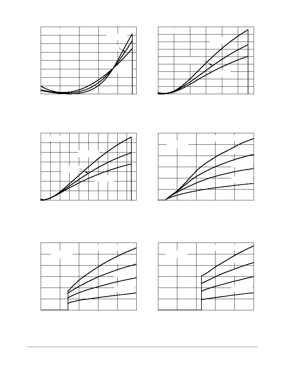
Figure 9. NCP300H/1L Series 0.9 V
Reset Output Sink Current versus Output Voltage
Figure 10. NCP300H/1L Series 2.7 V
Reset Output Sink Current versus Output Voltage
Figure 11. NCP300H/1L Series 4.5 V
Reset Output Sink Current versus Output Voltage
V
in
, INPUT VOLTAGE (V)
Figure 12. NCP300/1 Series 0.9 V
Input Current versus Input Voltage
0
2.0
6.0
8.0
10
2.0
1.5
1.0
0.5
0
V
in
, INPUT VOLTAGE (V)
4.0
2.5
Figure 13. NCP300/1 Series 2.7 V
Input Current versus Input Voltage
T
A
= 25
∞
C
Figure 14. NCP300/1 Series 4.5 V
Input Current versus Input Voltage
0
2.0
6.0
8.0
2.0
1.5
1.0
0.5
0
V
in
, INPUT VOLTAGE (V)
4.0
2.5
10
16
12
8.0
4.0
0
2.0
6.0
10
14
0
0.5
1.0
1.5
2.0
2.5
V
OUT
, OUTPUT VOLTAGE (V)
T
A
= 25
∞
C
V
in
= 4.0 V
V
in
= 3.5 V
V
in
= 3.0 V
V
in
= 2.5 V
V
in
= 2.0 V
V
in
= 1.5 V
I
OUT
, OUTPUT SINK CURRENT (mA)
I
OUT
, OUTPUT SINK CURRENT (mA)
V
in
= 2.5 V
V
in
= 2.0 V
V
in
= 1.5 V
T
A
= 25
∞
C
V
in
= 0.85 V
V
in
= 0.7 V
T
A
= 25
∞
C
5.5
11.8
0
0.2
0.4
0.6
0.8
1.0
1.2
0
2.0
4.0
6.0
8.0
10
T
A
= 25
∞
C
NCP300, NCP301
http://onsemi.com
14
I
OUT
, OUTPUT SOURCE CURRENT (mA)
I
OUT
, OUTPUT SOURCE CURRENT (mA)
I
OUT
, OUTPUT SOURCE CURRENT (mA)
I
OUT
, OUTPUT SINK CURRENT (mA)
I
OUT
, OUTPUT SINK CURRENT (mA)
I
OUT
, OUTPUT SINK CURRENT (mA)
V
in
, INPUT VOLTAGE (V)
Figure 15. NCP300H/1L Series 0.9 V
Reset Output Sink Current versus Input Voltage
1.2
0.8
0.4
0
0.2
0.6
1.0
1.6
0
0.2
0.4
0.6
0.8
1.0
V
in
, INPUT VOLTAGE (V)
Figure 16. NCP300H/1L Series 2.7 V
Reset Output Sink Current versus Input Voltage
0
9.0
5.0
3.0
1.0
0.5
1.0
1.5
2.0
2.5
3.0
2.0
0
4.0
8.0
V
in
, INPUT VOLTAGE (V)
Figure 17. NCP300H/1L Series 4.5 V
Reset Output Sink Current versus Input Voltage
0
1.0
2.0
3.0
4.0
5.0
14
6.0
4.0
0
2.0
8.0
10
Figure 18. NCP300L Series 0.9 V
Reset Output Source Current versus Input Voltage
10
8.0
2.0
0
0
2.0
4.0
6.0
8.0
10
V
in
, INPUT VOLTAGE (V)
4.0
6.0
12
V
OUT
= V
in
-2.1 V
Figure 19. NCP300L Series 2.7 V
Reset Output Source Current versus Input Voltage
10
8.0
0
0
2.0
4.0
6.0
8.0
10
V
in
, INPUT VOLTAGE (V)
2.0
4.0
6.0
12
V
OUT
= V
in
-2.1 V
Figure 20. NCP300L Series 4.5 V
Reset Output Source Current versus Input Voltage
10
8.0
0
0
2.0
4.0
6.0
8.0
10
V
in
, INPUT VOLTAGE (V)
2.0
4.0
6.0
12
V
OUT
= V
in
-2.1 V
T
A
= 25
∞
C
T
A
= -30
∞
C
T
A
= 85
∞
C
T
A
= 25
∞
C
T
A
= -30
∞
C
T
A
= 85
∞
C
T
A
= 25
∞
C
T
A
= -30
∞
C
T
A
= 85
∞
C
T
A
= 25
∞
C
V
in
-1.5 V
V
in
-1.0 V
V
in
-0.5 V
V
in
-1.5 V
V
in
-1.0 V
V
in
-0.5 V
T
A
= 25
∞
C
T
A
= 25
∞
C
V
in
-1.5 V
V
in
-1.0 V
V
in
-0.5 V
1.4
V
OUT
= 0.5 V
V
OUT
= 0.5 V
7.0
6.0
V
OUT
= 0.5 V
12
NCP300, NCP301
http://onsemi.com
15
OPERATING DESCRIPTION
The NCP300 and NCP301 series devices are second
generation ultra-low current voltage detectors. Figures 21
and 22 show a timing diagram and a typical application.
Initially consider that input voltage V
in
is at a nominal level
and it is greater than the voltage detector upper threshold
(V
DET+
), and the reset output (Pin 1) will be in the high state
for active low devices, or in the low state for active high
devices. If there is a power interruption and V
in
becomes
significantly deficient, it will fall below the lower detector
threshold (V
DET-
). This sequence of events causes the Reset
output to be in the low state for active low devices, or in the
high state for active high devices. After completion of the
power interruption, V
in
will again return to its nominal level
and become greater than the V
DET+
. The voltage detector
has built-in hysteresis to prevent erratic reset operation as
the comparator threshold is crossed.
Although these device series are specifically designed for
use as reset controllers in portable microprocessor based
systems, they offer a cost-effective solution in numerous
applications where precise voltage monitoring is required.
Figure 22 through Figure 29 shows various application
examples.
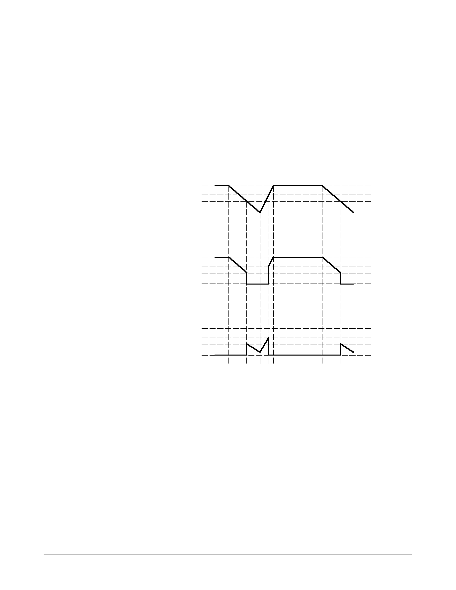
Figure 21. Timing Waveforms
V
in
V
DET
+
V
DET-
Input Voltage, Pin 2
V
in
0 V
Reset Output (Active Low), Pin 1
Reset Output (Active High), Pin 1
V
in
0 V
V
DET
+
V
DET-
V
DET
+
V
DET-
NCP300, NCP301
http://onsemi.com
16
APPLICATION CIRCUIT INFORMATION
Output
Figure 22. Microprocessor Reset Circuit
2
Input
1
Reset Output
GND
NCP300
LSN27T1
Figure 23. Battery Charge Indicator
2
Input
1
Reset Output
GND
GND
V
DD
Reset
V
DD
NCP300
Series
3
3
Microprocessor
*
Required for
NCP301
V
in
< 2.7 ON
V
in
> 2.835 ON
To Additional Circuitry
*
2.85 V
2.70 V
2
Input
1
Reset Output
GND
UV
NCP301
LSN23T1
Figure 24. Window Voltage Detector
3
V
supply
Fault
2
Input
1
Reset Output
GND
OV
NCP301
HSN43T1
3
Input
UV
Fault
UV
Fault
OV
Fault
OV
Fault
OK
OK
10 V
Active High
Device Thresholds
Active Low
Device Thresholds
1.0 V
The above circuit combines an active high and an active low reset output device to form
a window detector for monitoring battery or power supply voltages. When the input
voltage falls outside of the window established by the upper and lower device
thresholds, the LED will turn on indicating a fault. As the input voltage falls within the
window, increasing from 1.0 V and exceeding the active low device's hysteresis
threshold, or decreasing from the peak towards 1.0 V and falling below the active high
device's undervoltage threshold, the LED will turn off. The device thresholds shown can
be used for a single cell lithium-ion battery charge detector.

NCP300, NCP301
http://onsemi.com
17
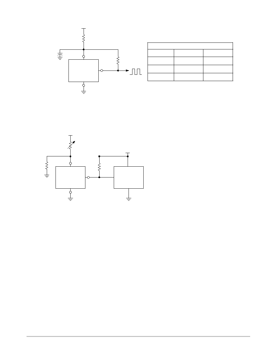
APPLICATION CIRCUIT INFORMATION
Low state output if either power
supply is below the respective
undervoltage detector threshold
but greater than 1.0 V.
2
1
NCP301
LSN45T1
Figure 25. Dual Power Supply Undervoltage Supervision
3
V
supply
2
1
NCP301
LSN30T1
3
3.3 V
5.0 V
Input
Reset Output
GND
Input
Reset Output
GND
Figure 26. Microprocessor Reset Circuit with Additional Hysteresis
2
1
NCP301
LSN27T1
3
V
DD
Reset Output
Input
R
H
R
L
NCP301
LSN27T1
GND
NCP301
LSN27T1
GND
Reset
V
DD
Microprocessor
Comparator hysteresis can be increased with the addition of
resistor R
H
. The hysteresis equations have been simplified and
do not account for the change of input current I
in
as V
in
crosses
the comparator threshold. The internal resistance, R
in
is simply
calculated using I
in
= 0.26
m
A at 2.6 V.
V
in
Decreasing:
V
th
+
R
H
R
in
)
1
V
DET
*
V
in
Increasing:
V
th
+
R
H
R
in
¯
R
L
)
1
V
DET
*
)
V
HYS
V
HYS
= V
in
Increasing - V
in
Decreasing
Test Data
V
th
Decreasing
(V)
V
th
Increasing
(V)
V
HYS
(V)
R
H
(
W
)
R
L
(k
W
)
¡¡¡¡¡¡
¡
¡¡¡¡
¡
¡
¡¡¡¡
¡
¡
¡¡¡¡
¡
¡
¡¡¡¡
¡
¡
¡¡¡¡
¡
¡
¡¡¡¡
¡
¡¡¡¡¡¡
2.70
2.70
2.70
2.70
2.70
2.70
2.70
2.70
2.70
2.70
¡¡¡¡¡¡
¡
¡¡¡¡
¡
¡
¡¡¡¡
¡
¡
¡¡¡¡
¡
¡
¡¡¡¡
¡
¡
¡¡¡¡
¡
¡
¡¡¡¡
¡
¡¡¡¡¡¡
2.84
2.87
2.88
2.91
2.90
2.94
2.98
2.70
3.04
3.15
¡¡¡
¡
¡
¡
¡
¡
¡
¡
¡
¡
¡
¡
¡
¡
¡
¡
¡
¡
¡
¡¡¡
0.135
0.17
0.19
0.21
0.20
0.24
0.28
0.27
0.34
0.35
¡¡¡
¡
¡
¡
¡
¡
¡
¡
¡
¡
¡
¡
¡
¡
¡
¡
¡
¡
¡
¡¡¡
0
100
100
100
220
220
220
470
470
470
¡¡
¡¡
¡¡
¡¡
¡¡
¡¡
¡¡
¡¡
-
10
6.8
4.3
10
6.8
4.3
10
6.8
4.3
NCP300, NCP301
http://onsemi.com
18
Figure 27. Simple Clock Oscillator
NCP301
LSN27T1
Reset Output
Input
82 k
NCP301
LSN27T1
GND
NCP300
HSN27T1
C
5.0 V
100 k
C (
m
F)
f
OSC
(kHz)
I
Q
(
m
A)
0.01
2590
21.77
0.1
490
21.97
1.0
52
22.07
Test Data
2
1
3
Figure 28. Microcontroller System Load Sensing
NCP301
LSN27T1
50 k
NCP301
LSN27T1
NCP301
LSN09T1
V
supply
Load
R
sense
Input
2
3
GND
1
Reset Output
Microcontroller
GND
V
DD
If:
I
Load
t
V
DET -
/R
sense
I
Load
w
(V
DET -
+V
HYS
)/R
sense
Then:
Reset Output = 0 V
Reset Output = V
DD
This circuit monitors the current at the load. As
current flows through the load, a voltage drop with
respect to ground appears across R
sense
where
V
sense
= I
load
* R
sense.
The following conditions apply:
NCP300, NCP301
http://onsemi.com
19
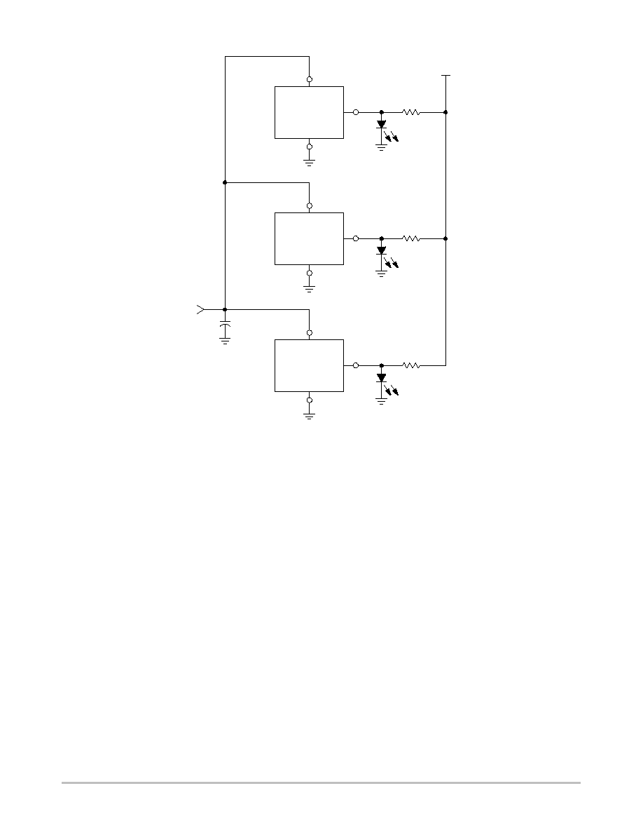
Figure 29. LED Bar Graph Voltage Monitor
NCP301
LSN27T1
2
NCP301
LSN27T1
NCP301
LSN45T1
3
1
V
supply
NCP301
LSN27T1
2
NCP301
LSN27T1
NCP301
LSN27T1
3
1
NCP301
LSN27T1
2
NCP301
LSN27T1
NCP301
LSN18T1
3
1
Input
GND
Reset
Output
Input
GND
Reset
Output
Input
GND
Reset
Output
V
in
= 1.0 V to 10 V
A simple voltage monitor can be constructed by connecting several voltage detectors as shown above. Each LED will
sequentially turn on when the respective voltage detector threshold (V
DET-
+V
HYS
) is exceeded. Note that detector
thresholds (V
DET-
) that range from 0.9 V to 4.9 V in 100 mV steps can be manufactured.
NCP300, NCP301
http://onsemi.com
20
ORDERING INFORMATION
Device
Threshold Voltage
Output Type
Reset
Marking
Package
Shipping
NCP300LSN09T1
0.9
SEJ
TSOP-5
NCP300LSN18T1
1.8
SFK
TSOP-5
NCP300LSN20T1
2.0
SHE
TSOP-5
NCP300LSN20T1G
2.0
SHE
TSOP-5
(Pb-Free)
NCP300LSN27T1
2.7
SEE
TSOP-5
NCP300LSN28T1
2.8
SED
TSOP-5
NCP300LSN28T1G
2.8
SED
TSOP-5
(Pb-Free)
NCP300LSN30T1
3.0
Active
Low
SEC
TSOP-5
NCP300LSN33T1
3.3
Low
SKV
TSOP-5
NCP300LSN34T1
3.4
SKU
TSOP-5
NCP300LSN44T1
4.4
SKK
TSOP-5
NCP300LSN45T1
4.5
SEA
TSOP-5
NCP300LSN46T1
4.6
CMOS
SKJ
TSOP-5
NCP300LSN47T1
4.7
SDZ
TSOP-5
NCP300LSN185T1
1.815
SRA
TSOP-5
NCP300LSN185T1G
1.815
SRA
TSOP-5
(Pb-Free)
3000 / Tape & Reel
NCP300HSN09T1
0.9
SDY
TSOP-5
3000 / Tape & Reel
(7 in. Reel)
NCP300HSN18T1
1.8
SFJ
TSOP-5
NCP300HSN18T1G
1.8
SFJ
TSOP-5
(Pb-Free)
NCP300HSN27T1
2.7
Active
SDU
TSOP-5
NCP300HSN27T1G
2.7
Active
High
SDU
TSOP-5
(Pb-Free)
NCP300HSN30T1
3.0
SDS
TSOP-5
NCP300HSN45T1
4.5
SDQ
TSOP-5
NCP300HSN47T1
4.7
SDP
TSOP-5
NCP301LSN09T1
0.9
SFF
TSOP-5
NCP301LSN12T1
1.2
SNN
TSOP-5
NCP301LSN12T1G
1.2
SNN
TSOP-5
(Pb-Free)
NCP301LSN16T1
1.6
Open
Drain
Active
Lo
SNJ
TSOP-5
NCP301LSN16T1G
1.6
Drain
Low
SNJ
TSOP-5
(Pb-Free)
NCP301LSN18T1
1.8
SFN
TSOP-5
NCP301LSN18T1G
1.8
SFN
TSOP-5
(Pb-Free)
NOTE:
The ordering information lists standard undervoltage thresholds with active low outputs. Additional active low threshold devices,
ranging from 0.9 V to 4.9 V in 100 mV increments and NCP300/NCP301 active high output devices, ranging from 0.9 V to 4.9 V
in 100 mV increments can be manufactured. Contact your ON Semiconductor representative for availability. The electrical
characteristics of these additional devices are shown in Tables 1 through 4.
For information on tape and reel specifications, including part orientation and tape sizes, please refer to our Tape and Reel Packaging Specifi-
cations Brochure, BRD8011/D.

NCP300, NCP301
http://onsemi.com
21
ORDERING INFORMATION
Device
Threshold Voltage
Output Type
Reset
Marking
Package
Shipping
NCP301LSN20T1
2.0
SFD
TSOP-5
NCP301LSN20T1G
2.0
SFD
TSOP-5
(Pb-Free)
NCP301LSN22T1
2.2
SNG
TSOP-5
NCP301LSN25T1
2.5
SNF
TSOP-5
NCP301LSN26T1
2.6
SNE
TSOP-5
NCP301LSN27T1
2.7
SFA
TSOP-5
NCP301LSN28T1
2.8
SEZ
TSOP-5
NCP301LSN28T1G
2.8
SEZ
TSOP-5
(Pb-Free)
NCP301LSN30T1
3.0
SEY
TSOP-5
NCP301LSN30T1G
3.0
Active
Low
SEY
TSOP-5
(Pb-Free)
NCP301LSN31T1
3.1
SEW
TSOP-5
NCP301LSN33T1
3.3
SNB
TSOP-5
NCP301LSN34T1
3.4
Open
Drain
SNA
TSOP-5
3000 / Tape & Reel
(7 in Reel)
NCP301LSN40T1
4.0
Drain
SMU
TSOP-5
(7 in. Reel)
NCP301LSN42T1
4.2
SMS
TSOP-5
NCP301LSN45T1
4.5
SEV
TSOP-5
NCP301LSN46T1
4.6
SMP
TSOP-5
NCP301LSN47T1
4.7
SEU
TSOP-5
NCP301LSN47T1G
4.7
SEU
TSOP-5
(Pb-Free)
NCP301HSN09T1
0.9
SET
TSOP-5
NCP301HSN18T1
1.8
SFM
TSOP-5
NCP301HSN22T1
2.2
SMD
TSOP-5
NCP301HSN27T1
2.7
Active
Hi h
SEP
TSOP-5
NCP301HSN27T1G
2.7
High
SEP
TSOP-5
(Pb-Free)
NCP301HSN30T1
3.0
SEN
TSOP-5
NCP301HSN45T1
4.5
SEL
TSOP-5
NOTE:
The ordering information lists standard undervoltage thresholds with active low outputs. Additional active low threshold devices,
ranging from 0.9 V to 4.9 V in 100 mV increments and NCP300/NCP301 active high output devices, ranging from 0.9 V to 4.9 V
in 100 mV increments can be manufactured. Contact your ON Semiconductor representative for availability. The electrical
characteristics of these additional devices are shown in Tables 1 through 4.
For information on tape and reel specifications, including part orientation and tape sizes, please refer to our Tape and Reel Packaging Specifi-
cations Brochure, BRD8011/D.

NCP300, NCP301
http://onsemi.com
22
PACKAGE DIMENSIONS
THIN SOT-23-5/TSOP-5/SC59-5
SN SUFFIX
PLASTIC PACKAGE
CASE 483-02
ISSUE C
NOTES:
1. DIMENSIONING AND TOLERANCING PER
ANSI Y14.5M, 1982.
2. CONTROLLING DIMENSION: MILLIMETER.
3. MAXIMUM LEAD THICKNESS INCLUDES
LEAD FINISH THICKNESS. MINIMUM LEAD
THICKNESS IS THE MINIMUM THICKNESS
OF BASE MATERIAL.
4. A AND B DIMENSIONS DO NOT INCLUDE
MOLD FLASH, PROTRUSIONS, OR GATE
BURRS.
DIM
MIN
MAX
MIN
MAX
INCHES
MILLIMETERS
A
2.90
3.10 0.1142 0.1220
B
1.30
1.70 0.0512 0.0669
C
0.90
1.10 0.0354 0.0433
D
0.25
0.50 0.0098 0.0197
G
0.85
1.05 0.0335 0.0413
H
0.013
0.100 0.0005 0.0040
J
0.10
0.26 0.0040 0.0102
K
0.20
0.60 0.0079 0.0236
L
1.25
1.55 0.0493 0.0610
M
0
10
0
10
S
2.50
3.00 0.0985 0.1181
0.05 (0.002)
1
2
3
5
4
S
A
G
L
B
D
H
C
K
M
J
_
_
_
_
0.7
0.028
1.0
0.039
mm
inches
SCALE 10:1
0.95
0.037
2.4
0.094
1.9
0.074
*For additional information on our Pb-Free strategy and soldering
details, please download the ON Semiconductor Soldering and
Mounting Techniques Reference Manual, SOLDERRM/D.
SOLDERING FOOTPRINT*
ON Semiconductor and are registered trademarks of Semiconductor Components Industries, LLC (SCILLC). SCILLC reserves the right to make changes without further notice
to any products herein. SCILLC makes no warranty, representation or guarantee regarding the suitability of its products for any particular purpose, nor does SCILLC assume any liability
arising out of the application or use of any product or circuit, and specifically disclaims any and all liability, including without limitation special, consequential or incidental damages.
"Typical" parameters which may be provided in SCILLC data sheets and/or specifications can and do vary in different applications and actual performance may vary over time. All
operating parameters, including "Typicals" must be validated for each customer application by customer's technical experts. SCILLC does not convey any license under its patent rights
nor the rights of others. SCILLC products are not designed, intended, or authorized for use as components in systems intended for surgical implant into the body, or other applications
intended to support or sustain life, or for any other application in which the failure of the SCILLC product could create a situation where personal injury or death may occur. Should
Buyer purchase or use SCILLC products for any such unintended or unauthorized application, Buyer shall indemnify and hold SCILLC and its officers, employees, subsidiaries, affiliates,
and distributors harmless against all claims, costs, damages, and expenses, and reasonable attorney fees arising out of, directly or indirectly, any claim of personal injury or death
associated with such unintended or unauthorized use, even if such claim alleges that SCILLC was negligent regarding the design or manufacture of the part. SCILLC is an Equal
Opportunity/Affirmative Action Employer. This literature is subject to all applicable copyright laws and is not for resale in any manner.
PUBLICATION ORDERING INFORMATION
N. American Technical Support: 800-282-9855 Toll Free
USA/Canada
Japan: ON Semiconductor, Japan Customer Focus Center
2-9-1 Kamimeguro, Meguro-ku, Tokyo, Japan 153-0051
Phone: 81-3-5773-3850
NCP300/D
LITERATURE FULFILLMENT:
Literature Distribution Center for ON Semiconductor
P.O. Box 61312, Phoenix, Arizona 85082-1312 USA
Phone: 480-829-7710 or 800-344-3860 Toll Free USA/Canada
Fax: 480-829-7709 or 800-344-3867 Toll Free USA/Canada
Email: orderlit@onsemi.com
ON Semiconductor Website: http://onsemi.com
Order Literature: http://www.onsemi.com/litorder
For additional information, please contact your
local Sales Representative.