
© Semiconductor Components Industries, LLC, 2005
March, 2005 - Rev. 16
1
Publication Order Number:
NCP304/D
NCP304, NCP305
Voltage Detector Series
The NCP304 and NCP305 series are second generation ultra-low
current voltage detectors. These devices are specifically designed for
use as reset controllers in portable microprocessor based systems
where extended battery life is paramount.
Each series features a highly accurate undervoltage detector with
hysteresis which prevents erratic system reset operation as the
comparator threshold is crossed.
The NCP304 series consists of complementary output devices that
are available with either an active high or active low reset output. The
NCP305 series has an open drain N-Channel output with an active low
reset output.
The NCP304 and NCP305 device series are available in the
SC-82AB package with standard undervoltage thresholds. Additional
thresholds that range from 0.9 V to 4.9 V in 100 mV steps can
be manufactured.
Features
∑
Quiescent Current of 1.0
mA Typical
∑
High Accuracy Undervoltage Threshold of 2.0%
∑
Wide Operating Voltage Range of 0.8 V to 10 V
∑
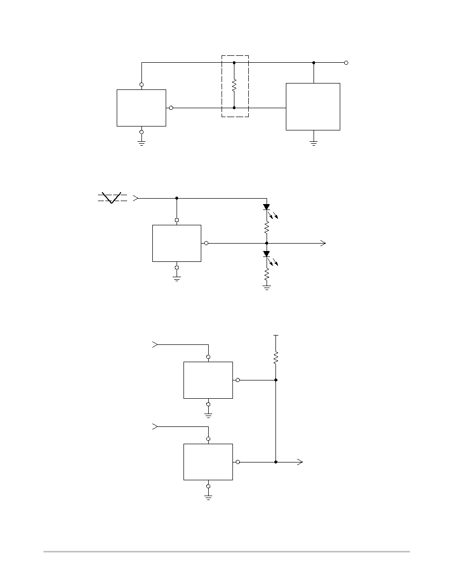
Complementary or Open Drain Reset Output
∑
Active Low or Active High Reset Output
∑
Pb-Free Packages are Available*
Typical Applications
∑
Microprocessor Reset Controller
∑
Low Battery Detection
∑
Power Fail Indicator
∑
Battery Backup Detection
NCP305LSQxxT1
Open Drain Output Configuration
NCP304xSQxxT1
Complementary Output Configuration
V
ref
V
ref
Input
Reset Output
GND
4
1
2
Input
Reset Output
GND
4
1
2
*
* The representative block diagram depicts active low reset output `L' suffix devices. The comparator
input is interchanged for the active high output `H' suffix devices.
This device contains 38 active transistors.
This device contains 37 active transistors.
Figure 1. Representative Block Diagrams
*For additional information on our Pb-Free strategy and soldering details, please
download the ON Semiconductor Soldering and Mounting Techniques
Reference Manual, SOLDERRM/D.
See detailed ordering and shipping information in the ordering
information section on page 20 of this data sheet.
ORDERING INFORMATION
SC-82AB
SQ SUFFIX
CASE 419C
PIN CONNECTIONS AND
MARKING DIAGRAM
4
1
1
4
3
2
V
in
Reset
Output
GND
N.C.
(Top View)
xxx = Specific Device Code
M
= Date Code
G
= Pb-Free Package
http://onsemi.com
xxxm
G
NCP304, NCP305
http://onsemi.com
2
MAXIMUM RATINGS
(Note 1)
Rating
Symbol
Value
Unit
Input Power Supply Voltage (Pin 2)
V
in
12
V
Output Voltage (Pin 1)
Complementary, NCP304
N-Channel Open Drain, NCP305
V
OUT
-0.3 to V
in
+0.3
-0.3 to 12
V
Output Current (Pin 1) (Note 2)
I
OUT
70
mA
Thermal Resistance Junction-to-Air
R
qJA
285
∞C/W
Maximum Junction Temperature
T
J
+125
∞C
Storage Temperature Range
T
stg
-55 to +150
∞C
Latchup Performance (Note 3)
Positive
Negative
I
LATCHUP
500
170
mA
Maximum ratings are those values beyond which device damage can occur. Maximum ratings applied to the device are individual stress limit
values (not normal operating conditions) and are not valid simultaneously. If these limits are exceeded, device functional operation is not implied,
damage may occur and reliability may be affected.
1. This device series contains ESD protection and exceeds the following tests:
Human Body Model 2000 V per MIL-STD-883, Method 3015.
Machine Model Method 200 V.
2. The maximum package power dissipation limit must not be exceeded.
PD +
TJ(max)-TA
RqJA
3. Maximum Ratings per JEDEC standard JESD78.
ELECTRICAL CHARACTERISTICS
(For all values T
A
= 25∞C, unless otherwise noted.)
Characteristic
Symbol
Min
Typ
Max
Unit
NCP304/5 - 0.9
Detector Threshold (Pin 2, V
in
Decreasing)
V
DET-
0.882
0.900
0.918
V
Detector Threshold Hysteresis (Pin 2, V
in
Increasing)
V
HYS
0.027
0.045
0.063
V
Supply Current (Pin 2)
(V
in
= 0.8 V)
(V
in
= 2.9 V)
I
in
-
-
0.8
-
2.4
3.0
mA
Maximum Operating Voltage (Pin 2)
V
in(max)
-
-
10
V
Minimum Operating Voltage (Pin 2)
(T
A
= -40∞C to 85∞C)
V
in(min)
-
-
0.55
0.65
0.70
0.80
V
Reset Output Current (Pin 1, Active Low `L' Suffix Devices)
I
OUT
mA
N-Channel Sink Current, NCP304, NCP305
(V
OUT
= 0.05 V, V
in
= 0.70 V)
(V
OUT
= 0.50 V, V
in
= 0.85 V)
0.01
0.05
0.05
0.50
-
-
P-Channel Source Current, NCP304
(V
OUT
= 2.4 V, V
in
= 4.5 V)
1.0
2.0
-
Reset Output Current (Pin 1, Active High `H' Suffix Devices)
I
OUT
mA
N-Channel Sink Current, NCP304, NCP305
(V
OUT
= 0.5 V, V
in
= 1.5 V)
1.05
2.5
-
P-Channel Source Current, NCP304
(V
OUT
= 0.4 V, V
in
= 0.7 V)
(V
OUT
= GND, V
in
= 0.8 V)
0.011
0.014
0.04
0.08
-
-
Propagation Delay Input to Output (Figure 2)
ms
4. In the case of CMOS Output Type: The time interval between the rising edge of V
DD
input pulse from 0.7 V to (+V
DET
) +2.0 V and output
voltage level becoming to V
DD
/2. In the case of N-Channel Open Drain Output Type: Output pin is pulled up with a resistance of 470 kW
to 5.0 V, the time interval between the rising edge of V
DD
input pulse from 0.7 V to (+V
DET
) +2.0 V and output voltage level becoming to
2.5 V.
NCP304, NCP305
http://onsemi.com
3
ELECTRICAL CHARACTERISTICS
(continued) (For all values T
A
= 25∞C, unless otherwise noted.)
Characteristic
Unit
Max
Typ
Min
Symbol
NCP304/5 - 0.9
Complementary Output NCP304 Series
Output Transition, High to Low (Note 4)
Output Transition, Low to High (Note 4)
t
pHL
t
pLH
-
-
18
6.0
-
60
N-Channel Open Drain NCP305 Series
Output Transition, High to Low (Note 4)
Output Transition, Low to High (Note 4)
t
pHL
t
pLH
-
-
18
-
-
100
NCP304/5 - 1.8
Detector Threshold (Pin 2, V
in
Decreasing)
V
DET-
1.764
1.80
1.836
V
Detector Threshold Hysteresis (Pin 2, V
in
Increasing)
V
HYS
0.054
0.090
0.126
V
Supply Current (Pin 2)
(V
in
= 1.7 V)
(V
in
= 3.8 V)
I
in
-
-
0.8
1.0
2.4
3.0
mA
Maximum Operating Voltage (Pin 2)
V
in(max)
-
-
10
V
Minimum Operating Voltage (Pin 2)
(T
A
= -40∞C to 85∞C)
V
in(min)
-
-
0.55
0.65
0.70
0.80
V
Reset Output Current (Pin 1, Active Low `L' Suffix Devices)
I
OUT
mA
N-Channel Sink Current, NCP304, NCP305
(V
OUT
= 0.05 V, V
in
= 0.70 V)
(V
OUT
= 0.50 V, V
in
= 1.5 V)
0.01
1.0
0.05
2.0
-
-
P-Channel Source Current, NCP304
(V
OUT
= 2.4 V, V
in
= 4.5 V)
1.0
2.0
-
Reset Output Current (Pin 1, Active High `H' Suffix Devices)
I
OUT
mA
N-Channel Sink Current, NCP304, NCP305
(V
OUT
= 0.5 V, V
in
= 5.0 V)
6.3
11
-
P-Channel Source Current, NCP304
(V
OUT
= 0.4 V, V
in
= 0.7 V)
(V
OUT
= GND, V
in
= 1.5 V)
0.011
0.525
0.04
0.6
-
-
Propagation Delay Input to Output (Figure 2)
ms
Complementary Output NCP304 Series
Output Transition, High to Low (Note 4)
Output Transition, Low to High (Note 4)
t
pHL
t
pLH
-
-
14
15
-
60
N-Channel Open Drain NCP305 Series
Output Transition, High to Low (Note 4)
Output Transition, Low to High (Note 4)
t
pHL
t
pLH
-
-
14
-
-
100
NCP304/5 - 2.0
Detector Threshold (Pin 2, V
in
Decreasing)
V
DET-
1.960
2.00
2.040
V
Detector Threshold Hysteresis (Pin 2, V
in
Increasing)
V
HYS
0.06
0.10
0.14
V
Supply Current (Pin 2)
(V
in
= 1.9 V)
(V
in
= 4.0 V)
I
in
-
-
0.9
1.1
2.7
3.3
mA
Maximum Operating Voltage (Pin 2)
V
in(max)
-
-
10
V
Minimum Operating Voltage (Pin 2)
(T
A
= -40∞C to 85∞C)
V
in(min)
-
-
0.55
0.65
0.70
0.80
V
Reset Output Current (Pin 1, Active Low `L' Suffix Devices)
I
OUT
mA
4. In the case of CMOS Output Type: The time interval between the rising edge of V
DD
input pulse from 0.7 V to (+V
DET
) +2.0 V and output
voltage level becoming to V
DD
/2. In the case of N-Channel Open Drain Output Type: Output pin is pulled up with a resistance of 470 kW
to 5.0 V, the time interval between the rising edge of V
DD
input pulse from 0.7 V to (+V
DET
) +2.0 V and output voltage level becoming to
2.5 V.

NCP304, NCP305
http://onsemi.com
4
ELECTRICAL CHARACTERISTICS
(continued) (For all values T
A
= 25∞C, unless otherwise noted.)
Characteristic
Unit
Max
Typ
Min
Symbol
NCP304/5 - 2.0
N-Channel Sink Current, NCP304, NCP305
(V
OUT
= 0.05 V, V
in
= 0.70 V)
(V
OUT
= 0.50 V, V
in
= 1.5 V)
0.01
1.0
0.05
2.0
-
-
P-Channel Source Current, NCP304
(V
OUT
= 2.4 V, V
in
= 4.5 V)
1.0
2.0
-
Reset Output Current (Pin 1, Active High `H' Suffix Devices)
I
OUT
mA
N-Channel Sink Current, NCP304, NCP305
(V
OUT
= 0.5 V, V
in
= 5.0 V)
6.3
11
-
P-Channel Source Current, NCP304
(V
OUT
= 0.4 V, V
in
= 0.7 V)
(V
OUT
= GND, V
in
= 1.5 V)
0.011
0.525
0.04
0.6
-
-
Propagation Delay Input to Output (Figure 2)
ms
Complementary Output NCP304 Series
Output Transition, High to Low (Note 4)
Output Transition, Low to High (Note 4)
t
pHL
t
pLH
-
-
13
15
-
60
N-Channel Open Drain NCP305 Series
Output Transition, High to Low (Note 4)
Output Transition, Low to High (Note 4)
t
pHL
t
pLH
-
-
13
-
-
100
NCP304/5 - 2.7
Detector Threshold (Pin 2, V
in
Decreasing)
V
DET-
2.646
2.700
2.754
V
Detector Threshold Hysteresis (Pin 2, V
in
Increasing)
V
HYS
0.081
0.135
0.189
V
Supply Current (Pin 2)
(V
in
= 2.6 V)
(V
in
= 4.7 V)
I
in
-
-
0.9
1.1
2.7
3.3
mA
Maximum Operating Voltage (Pin 2)
V
in(max)
-
-
10
V
Minimum Operating Voltage (Pin 2)
(T
A
= -40∞C to 85∞C)
V
in(min)
-
-
0.55
0.65
0.70
0.80
V
Reset Output Current (Pin 1, Active Low `L' Suffix Devices)
I
OUT
mA
N-Channel Sink Current, NCP304, NCP305
(V
OUT
= 0.05 V, V
in
= 0.70 V)
(V
OUT
= 0.50 V, V
in
= 1.5 V)
0.01
1.0
0.05
2.0
-
-
P-Channel Source Current, NCP304
(V
OUT
= 2.4 V, V
in
= 4.5 V)
1.0
2.0
-
Reset Output Current (Pin 1, Active High `H' Suffix Devices)
I
OUT
mA
N-Channel Sink Current, NCP304, NCP305
(V
OUT
= 0.5 V, V
in
= 5.0 V)
6.3
11
-
P-Channel Source Current, NCP304
(V
OUT
= 0.4 V, V
in
= 0.7 V)
(V
OUT
= GND, V
in
= 1.5 V)
0.011
0.525
0.04
0.6
-
-
Propagation Delay Input to Output (Figure 2)
ms
Complementary Output NCP304 Series
Output Transition, High to Low (Note 4)
Output Transition, Low to High (Note 4)
t
pHL
t
pLH
-
-
12
19
-
60
N-Channel Open Drain NCP305 Series
Output Transition, High to Low (Note 4)
Output Transition, Low to High (Note 4)
t
pHL
t
pLH
-
-
12
-
-
100
4. In the case of CMOS Output Type: The time interval between the rising edge of V
DD
input pulse from 0.7 V to (+V
DET
) +2.0 V and output
voltage level becoming to V
DD
/2. In the case of N-Channel Open Drain Output Type: Output pin is pulled up with a resistance of 470 kW
to 5.0 V, the time interval between the rising edge of V
DD
input pulse from 0.7 V to (+V
DET
) +2.0 V and output voltage level becoming to
2.5 V.
NCP304, NCP305
http://onsemi.com
5
ELECTRICAL CHARACTERISTICS
(continued) (For all values T
A
= 25∞C, unless otherwise noted.)
Characteristic
Unit
Max
Typ
Min
Symbol
NCP304/5 - 2.9
Detector Threshold (Pin 2, V
in
Decreasing)
V
DET-
2.842
2.900
2.958
V
Detector Threshold Hysteresis (Pin 2, V
in
Increasing)
V
HYS
0.087
0.145
0.203
V
Supply Current (Pin 2)
(V
in
= 2.8 V)
(V
in
= 4.9 V)
I
in
-
-
0.9
1.1
2.9
3.5
mA
Maximum Operating Voltage (Pin 2)
V
in(max)
-
-
10
V
Minimum Operating Voltage (Pin 2)
(T
A
= -40∞C to 85∞C)
V
in(min)
-
-
0.55
0.65
0.70
0.80
V
Reset Output Current (Pin 1, Active Low `L' Suffix Devices)
I
OUT
mA
N-Channel Sink Current, NCP304, NCP305
(V
OUT
= 0.05 V, V
in
= 0.70 V)
(V
OUT
= 0.50 V, V
in
= 1.5 V)
0.01
1.0
0.05
2.0
-
-
P-Channel Source Current, NCP304
(V
OUT
= 2.4 V, V
in
= 4.5 V)
1.0
2.0
-
Reset Output Current (Pin 1, Active High `H' Suffix Devices)
I
OUT
mA
N-Channel Sink Current, NCP304, NCP305
(V
OUT
= 0.5 V, V
in
= 5.0 V)
6.3
11
-
P-Channel Source Current, NCP304
(V
OUT
= 0.4 V, V
in
= 0.7 V)
(V
OUT
= GND, V
in
= 1.5 V)
0.011
0.525
0.04
0.6
-
-
Propagation Delay Input to Output (Figure 2)
ms
Complementary Output NCP304 Series
Output Transition, High to Low (Note 4)
Output Transition, Low to High (Note 4)
t
pHL
t
pLH
-
-
12
19
-
60
N-Channel Open Drain NCP305 Series
Output Transition, High to Low (Note 4)
Output Transition, Low to High (Note 4)
t
pHL
t
pLH
-
-
12
-
-
100
NCP304/5 - 3.0
Detector Threshold (Pin 2, V
in
Decreasing)
V
DET-
2.94
3.00
3.06
V
Detector Threshold Hysteresis (Pin 2, V
in
Increasing)
V
HYS
0.09
0.15
0.21
V
Supply Current (Pin 2)
(V
in
= 2.87 V)
(V
in
= 5.0 V)
I
in
-
-
1.0
1.2
3.0
3.6
mA
Maximum Operating Voltage (Pin 2)
V
in(max)
-
-
10
V
Minimum Operating Voltage (Pin 2)
(T
A
= -40∞C to 85∞C)
V
in(min)
-
-
0.55
0.65
0.70
0.80
V
Reset Output Current (Pin 1, Active Low `L' Suffix Devices)
I
OUT
mA
N-Channel Sink Current, NCP304, NCP305
(V
OUT
= 0.05 V, V
in
= 0.70 V)
(V
OUT
= 0.50 V, V
in
= 1.5 V)
0.01
1.0
0.05
2.0
-
-
P-Channel Source Current, NCP304
(V
OUT
= 2.4 V, V
in
= 4.5 V)
1.0
2.0
-
Reset Output Current (Pin 1, Active High `H' Suffix Devices)
I
OUT
mA
N-Channel Sink Current, NCP304, NCP305
(V
OUT
= 0.5 V, V
in
= 5.0 V)
6.3
11
-
4. In the case of CMOS Output Type: The time interval between the rising edge of V
DD
input pulse from 0.7 V to (+V
DET
) +2.0 V and output
voltage level becoming to V
DD
/2. In the case of N-Channel Open Drain Output Type: Output pin is pulled up with a resistance of 470 kW
to 5.0 V, the time interval between the rising edge of V
DD
input pulse from 0.7 V to (+V
DET
) +2.0 V and output voltage level becoming to
2.5 V.
NCP304, NCP305
http://onsemi.com
6
ELECTRICAL CHARACTERISTICS
(continued) (For all values T
A
= 25∞C, unless otherwise noted.)
Characteristic
Unit
Max
Typ
Min
Symbol
NCP304/5 - 3.0
P-Channel Source Current, NCP304
(V
OUT
= 0.4 V, V
in
= 0.7 V)
(V
OUT
= GND, V
in
= 1.5 V)
0.011
0.525
0.04
0.6
-
-
Propagation Delay Input to Output (Figure 2)
ms
Complementary Output NCP304 Series
Output Transition, High to Low (Note 4)
Output Transition, Low to High (Note 4)
t
pHL
t
pLH
-
-
12
19
-
60
N-Channel Open Drain NCP305 Series
Output Transition, High to Low (Note 4)
Output Transition, Low to High (Note 4)
t
pHL
t
pLH
-
-
12
-
-
100
NCP304/5 - 4.5
Detector Threshold (Pin 2, V
in
Decreasing)
V
DET-
4.410
4.500
4.590
V
Detector Threshold Hysteresis (Pin 2, V
in
Increasing)
V
HYS
0.135
0.225
0.315
V
Supply Current (Pin 2)
(V
in
= 4.34 V)
(V
in
= 6.5 V)
I
in
-
-
-
-
3.0
3.9
mA
Maximum Operating Voltage (Pin 2)
V
in(max)
-
-
10
V
Minimum Operating Voltage (Pin 2)
(T
A
= -40∞C to 85∞C)
V
in(min)
-
-
0.55
0.65
0.70
0.80
V
Reset Output Current (Pin 1, Active Low `L' Suffix Devices)
I
OUT
mA
N-Channel Sink Current, NCP304, NCP305
(V
OUT
= 0.05 V, V
in
= 0.70 V)
(V
OUT
= 0.50 V, V
in
= 1.5 V)
0.01
1.0
0.05
2.0
-
-
P-Channel Source Current, NCP304
(V
OUT
= 5.9 V, V
in
= 8.0 V)
1.5
3.0
-
Reset Output Current (Pin 1, Active High `H' Suffix Devices)
I
OUT
mA
N-Channel Sink Current, NCP304, NCP305
(V
OUT
= 0.5 V, V
in
= 5.0 V)
6.3
11
-
P-Channel Source Current, NCP304
(V
OUT
= 0.4 V, V
in
= 0.7 V)
(V
OUT
= GND, V
in
= 1.5 V)
0.011
0.525
0.04
0.6
-
-
Propagation Delay Input to Output (Figure 2)
ms
Complementary Output NCP304 Series
Output Transition, High to Low (Note 4)
Output Transition, Low to High (Note 4)
t
pHL
t
pLH
-
-
10
21
-
60
N-Channel Open Drain NCP305 Series
Output Transition, High to Low (Note 4)
Output Transition, Low to High (Note 4)
t
pHL
t
pLH
-
-
10
-
-
100
NCP304/5 - 4.7
Detector Threshold (Pin 2, V
in
Decreasing)
V
DET-
4.606
4.70
4.794
V
Detector Threshold Hysteresis (Pin 2, V
in
Increasing)
V
HYS
0.141
0.235
0.329
V
Supply Current (Pin 2)
(V
in
= 4.54 V)
(V
in
= 6.7 V)
I
in
-
-
1.1
1.3
3.0
3.9
mA
Maximum Operating Voltage (Pin 2)
V
in(max)
-
-
10
V
4. In the case of CMOS Output Type: The time interval between the rising edge of V
DD
input pulse from 0.7 V to (+V
DET
) +2.0 V and output
voltage level becoming to V
DD
/2. In the case of N-Channel Open Drain Output Type: Output pin is pulled up with a resistance of 470 kW
to 5.0 V, the time interval between the rising edge of V
DD
input pulse from 0.7 V to (+V
DET
) +2.0 V and output voltage level becoming to
2.5 V.

NCP304, NCP305
http://onsemi.com
7
ELECTRICAL CHARACTERISTICS
(continued) (For all values T
A
= 25∞C, unless otherwise noted.)
Characteristic
Unit
Max
Typ
Min
Symbol
NCP304/5 - 4.7
Minimum Operating Voltage (Pin 2)
(T
A
= -40∞C to 85∞C)
V
in(min)
-
-
0.55
0.65
0.70
0.80
V
Reset Output Current (Pin 1, Active Low `L' Suffix Devices)
I
OUT
mA
N-Channel Sink Current, NCP304, NCP305
(V
OUT
= 0.05 V, V
in
= 0.70 V)
(V
OUT
= 0.50 V, V
in
= 1.5 V)
0.01
1.0
0.05
2.0
-
-
P-Channel Source Current, NCP304
(V
OUT
= 5.9 V, V
in
= 8.0 V)
1.5
3.0
-
Reset Output Current (Pin 1, Active High `H' Suffix Devices)
I
OUT
mA
N-Channel Sink Current, NCP304, NCP305
(V
OUT
= 0.5 V, V
in
= 5.0 V)
6.3
11
-
P-Channel Source Current, NCP304
(V
OUT
= 0.4 V, V
in
= 0.7 V)
(V
OUT
= GND, V
in
= 1.5 V)
0.011
0.525
0.04
0.6
-
-
Propagation Delay Input to Output (Figure 2)
ms
Complementary Output NCP304 Series
Output Transition, High to Low (Note 4)
Output Transition, Low to High (Note 4)
t
pHL
t
pLH
-
-
10
21
-
60
N-Channel Open Drain NCP305 Series
Output Transition, High to Low (Note 4)
Output Transition, Low to High (Note 4)
t
pHL
t
pLH
-
-
10
-
-
100
4. In the case of CMOS Output Type: The time interval between the rising edge of V
DD
input pulse from 0.7 V to (+V
DET
) +2.0 V and output
voltage level becoming to V
DD
/2. In the case of N-Channel Open Drain Output Type: Output pin is pulled up with a resistance of 470 kW
to 5.0 V, the time interval between the rising edge of V
DD
input pulse from 0.7 V to (+V
DET
) +2.0 V and output voltage level becoming to
2.5 V.

NCP304, NCP305
http://onsemi.com
8
Figure 2. Propagation Delay Measurement Conditions
NCP304 and NCP305 series are measured with a 10 pF capacitive load. NCP305 has an additional 470 k pullup resistor connected
from the reset output to +5.0 V. The reset output voltage waveforms are shown for the active low `L' devices. The upper detector
threshold, V
DET+
is the sum of the lower detector threshold, V
DET-
plus the input hysteresis, V
HYS
.
Input Voltage, Pin 2
Reset Output Voltage, Pin 1
0.7
0 V
5 V
0 V
0.5 V
2.5 V
NCP304L
Complementary
NCP305L
Open Drain
t
pLH
t
pHL
0.1 V
Reset Output Voltage, Pin 1
0 V
V
DET+
+ 2
V
DET+
+ 2
V
DET+
+ 2
2

NCP304, NCP305
http://onsemi.com
9
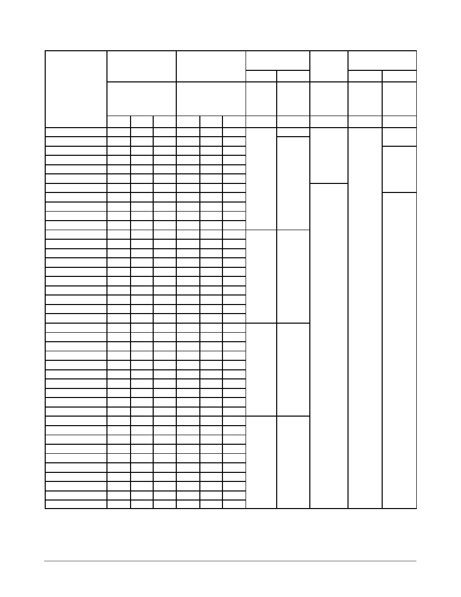
Table 1. NCP304 SERIES ELECTRICAL CHARACTERISTIC TABLE FOR 0.9 - 4.9 V
Detector Threshold
Supply Current
N-Channel Sink Cur-
rent
P-Channel
Source
Detector Threshold
Detector Threshold
Hysteresis
V
in
Low
V
in
High
V
in
Low
V
in
High
Source
Current
V
DET-
(V)
V
HYS
(V)
I
in
(mA)
(Note 5)
I
in
(mA)
(Note 6)
I
OUT
(mA)
(Note 7)
I
OUT
(mA)
(Note 8)
I
OUT
(mA)
(Note 9)
Part Number
Min
Typ
Max
Min
Typ
Max
Typ
Typ
Typ
Typ
Typ
NCP304LSQ09T1
0.882
0.9
0.918
0.027
0.045
0.063
0.8
0.9
0.05
0.5
2.0
NCP304LSQ10T1
0.980
1.0
1.020
0.030
0.050
0.070
1.0
NCP304LSQ11T1
1.078
1.1
1.122
0.033
0.055
0.077
1.0
NCP304LSQ12T1
1.176
1.2
1.224
0.036
0.060
0.084
NCP304LSQ13T1
1.274
1.3
1.326
0.039
0.065
0.091
NCP304LSQ14T1
1.372
1.4
1.428
0.042
0.070
0.098
NCP304LSQ15T1
1.470
1.5
1.530
0.045
0.075
0.105
NCP304LSQ16T1
1.568
1.6
1.632
0.048
0.080
0.112
2.0
NCP304LSQ17T1
1.666
1.7
1.734
0.051
0.085
0.119
NCP304LSQ18T1
1.764
1.8
1.836
0.054
0.090
0.126
NCP304LSQ19T1
1.862
1.9
1.938
0.057
0.095
0.133
NCP304LSQ20T1
1.960
2.0
2.040
0.060
0.100
0.140
0.9
1.1
NCP304LSQ21T1
2.058
2.1
2.142
0.063
0.105
0.147
NCP304LSQ22T1
2.156
2.2
2.244
0.066
0.110
0.154
NCP304LSQ23T1
2.254
2.3
2.346
0.069
0.115
0.161
NCP304LSQ24T1
2.352
2.4
2.448
0.072
0.120
0.168
NCP304LSQ25T1
2.450
2.5
2.550
0.075
0.125
0.175
NCP304LSQ26T1
2.548
2.6
2.652
0.078
0.130
0.182
NCP304LSQ27T1
2.646
2.7
2.754
0.081
0.135
0.189
NCP304LSQ28T1
2.744
2.8
2.856
0.084
0.140
0.196
NCP304LSQ29T1
2.842
2.9
2.958
0.087
0.145
0.203
NCP304LSQ30T1
2.940
3.0
3.060
0.090
0.150
0.210
1.0
1.2
NCP304LSQ31T1
3.038
3.1
3.162
0.093
0.155
0.217
NCP304LSQ32T1
3.136
3.2
3.264
0.096
0.160
0.224
NCP304LSQ33T1
3.234
3.3
3.366
0.099
0.165
0.231
NCP304LSQ34T1
3.332
3.4
3.468
0.102
0.170
0.238
NCP304LSQ35T1
3.430
3.5
3.570
0.105
0.175
0.245
NCP304LSQ36T1
3.528
3.6
3.672
0.108
0.180
0.252
NCP304LSQ37T1
3.626
3.7
3.774
0.111
0.185
0.259
NCP304LSQ38T1
3.724
3.8
3.876
0.114
0.190
0.266
NCP304LSQ39T1
3.822
3.9
3.978
0.117
0.195
0.273
NCP304LSQ40T1
3.920
4.0
4.080
0.120
0.200
0.280
1.1
1.3
3.0
NCP304LSQ41T1
4.018
4.1
4.182
0.123
0.205
0.287
NCP304LSQ42T1
4.116
4.2
4.284
0.126
0.210
0.294
NCP304LSQ43T1
4.214
4.3
4.386
0.129
0.215
0.301
NCP304LSQ44T1
4.312
4.4
4.488
0.132
0.220
0.308
NCP304LSQ45T1
4.410
4.5
4.590
0.135
0.225
0.315
NCP304LSQ46T1
4.508
4.6
4.692
0.138
0.230
0.322
NCP304LSQ47T1
4.606
4.7
4.794
0.141
0.235
0.329
NCP304LSQ48T1
4.704
4.8
4.896
0.144
0.240
0.336
NCP304LSQ49T1
4.802
4.9
4.998
0.147
0.245
0.343
5. Condition 1: 0.9 - 2.9 V, V
in
= V
DET-
- 0.10 V; 3.0 - 3.9 V, V
in
= V
DET-
- 0.13 V; 4.0 - 4.9 V, V
in
= V
DET-
- 0.16 V
6. Condition 2: 0.9 - 4.9 V, V
in
= V
DET-
+ 2.0 V
7. Condition 3: 0.9 - 4.9 V, V
in
= 0.7 V, V
OUT
= 0.05 V, Active Low `L' Suffix Devices
8. Condition 4: 0.9 - 1.0 V, V
in
= 0.85 V, V
OUT
= 0.5 V; 1.1 - 1.5 V, V
in
= 1.0 V, V
OUT
= 0.5 V; 1.6 - 4.9 V, V
in
= 1.5 V, V
OUT
= 0.5 V,
Condition 4:
Active Low `L' Suffix Devices
9. Condition 5: 0.9 - 3.9 V, V
in
= 4.5 V, V
OUT
= 2.4 V; 4.0 - 4.9 V, V
in
= 8.0 V, V
OUT
= 5.9 V, Active Low `L' Suffix Devices
NCP304, NCP305
http://onsemi.com
10
Table 2. NCP304 SERIES ELECTRICAL CHARACTERISTIC TABLE FOR 0.9 - 4.9 V
Detector Threshold
Supply Current
N-Channel
Sink
P-Channel
Source Current
Detector Threshold
Detector Threshold
Hysteresis
V
in
Low
V
in
High
Sink
Current
V
in
Low
V
in
High
V
DET-
(V)
V
HYS
(V)
I
in
(mA)
(Note 10
)
I
in
(mA)
(Note 11)
I
OUT
(mA)
(Note 12)
I
OUT
(mA)
(Note 13)
I
OUT
(mA)
(Note 14)
Part Number
Min
Typ
Max
Min
Typ
Max
Typ
Typ
Typ
Typ
Typ
NCP304HSQ09T1
0.882
0.9
0.918
0.027
0.045
0.063
0.8
0.9
2.5
0.04
0.08
NCP304HSQ10T1
0.980
1.0
1.020
0.030
0.050
0.070
1.0
NCP304HSQ11T1
1.078
1.1
1.122
0.033
0.055
0.077
0.18
NCP304HSQ12T1
1.176
1.2
1.224
0.036
0.060
0.084
NCP304HSQ13T1
1.274
1.3
1.326
0.039
0.065
0.091
NCP304HSQ14T1
1.372
1.4
1.428
0.042
0.070
0.098
NCP304HSQ15T1
1.470
1.5
1.530
0.045
0.075
0.105
11
NCP304HSQ16T1
1.568
1.6
1.632
0.048
0.080
0.112
0.6
NCP304HSQ17T1
1.666
1.7
1.734
0.051
0.085
0.119
NCP304HSQ18T1
1.764
1.8
1.836
0.054
0.090
0.126
NCP304HSQ19T1
1.862
1.9
1.938
0.057
0.095
0.133
NCP304HSQ20T1
1.960
2.0
2.040
0.060
0.100
0.140
0.9
1.1
NCP304HSQ21T1
2.058
2.1
2.142
0.063
0.105
0.147
NCP304HSQ22T1
2.156
2.2
2.244
0.066
0.110
0.154
NCP304HSQ23T1
2.254
2.3
2.346
0.069
0.115
0.161
NCP304HSQ24T1
2.352
2.4
2.448
0.072
0.120
0.168
NCP304HSQ25T1
2.450
2.5
2.550
0.075
0.125
0.175
NCP304HSQ26T1
2.548
2.6
2.652
0.078
0.130
0.182
NCP304HSQ27T1
2.646
2.7
2.754
0.081
0.135
0.189
NCP304HSQ28T1
2.744
2.8
2.856
0.084
0.140
0.196
NCP304HSQ29T1
2.842
2.9
2.958
0.087
0.145
0.203
NCP304HSQ30T1
2.940
3.0
3.060
0.090
0.150
0.210
1.0
1.2
NCP304HSQ31T1
3.038
3.1
3.162
0.093
0.155
0.217
NCP304HSQ32T1
3.136
3.2
3.264
0.096
0.160
0.224
NCP304HSQ33T1
3.234
3.3
3.366
0.099
0.165
0.231
NCP304HSQ34T1
3.332
3.4
3.468
0.102
0.170
0.238
NCP304HSQ35T1
3.430
3.5
3.570
0.105
0.175
0.245
NCP304HSQ36T1
3.528
3.6
3.672
0.108
0.180
0.252
NCP304HSQ37T1
3.626
3.7
3.774
0.111
0.185
0.259
NCP304HSQ38T1
3.724
3.8
3.876
0.114
0.190
0.266
NCP304HSQ39T1
3.822
3.9
3.978
0.117
0.195
0.273
NCP304HSQ40T1
3.920
4.0
4.080
0.120
0.200
0.280
1.1
1.3
NCP304HSQ41T1
4.018
4.1
4.182
0.123
0.205
0.287
NCP304HSQ42T1
4.116
4.2
4.284
0.126
0.210
0.294
NCP304HSQ43T1
4.214
4.3
4.386
0.129
0.215
0.301
NCP304HSQ44T1
4.312
4.4
4.488
0.132
0.220
0.308
NCP304HSQ45T1
4.410
4.5
4.590
0.135
0.225
0.315
NCP304HSQ46T1
4.508
4.6
4.692
0.138
0.230
0.322
NCP304HSQ47T1
4.606
4.7
4.794
0.141
0.235
0.329
NCP304HSQ48T1
4.704
4.8
4.896
0.144
0.240
0.336
NCP304HSQ49T1
4.802
4.9
4.998
0.147
0.245
0.343
10.Condition 1: 0.9 - 2.9 V, V
in
= V
DET-
- 0.10 V; 3.0 - 3.9 V, V
in
= V
DET-
- 0.13 V; 4.0 - 4.9 V, V
in
= V
DET-
- 0.16 V
11. Condition 2: 0.9 - 4.9 V, V
in
= V
DET-
+ 2.0 V
12.Condition 3: 0.9 - 1.4 V, V
in
= 1.5 V, V
OUT
= 0.5 V; 1.5 - 4.9 V, V
in
= 5.0 V, V
OUT
= 0.5 V, Active High `H' Suffix Devices
13.Condition 4: 0.9 - 4.9 V, V
in
= 0.7 V, V
OUT
= 0.4 V, Active High `H' Suffix Devices
14.Condition 5: 0.9 - 1.0 V, V
in
= 0.8 V, V
OUT
= GND; 1.1 - 1.5 V, V
in
= 1.0 V, V
OUT
= GND; 1.6 - 4.9 V, V
in
= 1.5 V, V
OUT
= GND,
Active High `H' Suffix Devices

NCP304, NCP305
http://onsemi.com
11
Table 3. NCP305 SERIES ELECTRICAL CHARACTERISTIC TABLE FOR 0.9 - 4.9 V
Detector Threshold
Supply Current
N-Channel
Sink Current
Detector Threshold
Detector Threshold
Hysteresis
V
in
Low
V
in
High
V
in
Low
V
in
High
V
DET-
(V)
V
HYS
(V)
I
in
(mA)
(Note 15)
I
in
(mA)
(Note 16)
I
OUT
(mA)
(Note 17)
I
OUT
(mA)
(Note 18)
Part Number
Min
Typ
Max
Min
Typ
Max
Typ
Typ
Typ
Typ
NCP305LSQ09T1
0.882
0.9
0.918
0.027
0.045
0.063
0.8
0.9
0.05
0.5
NCP305LSQ10T1
0.980
1.0
1.020
0.030
0.050
0.070
1.0
NCP305LSQ11T1
1.078
1.1
1.122
0.033
0.055
0.077
1.0
NCP305LSQ12T1
1.176
1.2
1.224
0.036
0.060
0.084
NCP305LSQ13T1
1.274
1.3
1.326
0.039
0.065
0.091
NCP305LSQ14T1
1.372
1.4
1.428
0.042
0.070
0.098
NCP305LSQ15T1
1.470
1.5
1.530
0.045
0.075
0.105
NCP305LSQ16T1
1.568
1.6
1.632
0.048
0.080
0.112
2.0
NCP305LSQ17T1
1.666
1.7
1.734
0.051
0.085
0.119
NCP305LSQ18T1
1.764
1.8
1.836
0.054
0.090
0.126
NCP305LSQ19T1
1.862
1.9
1.938
0.057
0.095
0.133
NCP305LSQ20T1
1.960
2.0
2.040
0.060
0.100
0.140
0.9
1.1
NCP305LSQ21T1
2.058
2.1
2.142
0.063
0.105
0.147
NCP305LSQ22T1
2.156
2.2
2.244
0.066
0.110
0.154
NCP305LSQ23T1
2.254
2.3
2.346
0.069
0.115
0.161
NCP305LSQ24T1
2.352
2.4
2.448
0.072
0.120
0.168
NCP305LSQ25T1
2.450
2.5
2.550
0.075
0.125
0.175
NCP305LSQ26T1
2.548
2.6
2.652
0.078
0.130
0.182
NCP305LSQ27T1
2.646
2.7
2.754
0.081
0.135
0.189
NCP305LSQ28T1
2.744
2.8
2.856
0.084
0.140
0.196
NCP305LSQ29T1
2.842
2.9
2.958
0.087
0.145
0.203
NCP305LSQ30T1
2.940
3.0
3.060
0.090
0.150
0.210
1.0
1.2
NCP305LSQ31T1
3.038
3.1
3.162
0.093
0.155
0.217
NCP305LSQ32T1
3.136
3.2
3.264
0.096
0.160
0.224
NCP305LSQ33T1
3.234
3.3
3.366
0.099
0.165
0.231
NCP305LSQ34T1
3.332
3.4
3.468
0.102
0.170
0.238
NCP305LSQ35T1
3.430
3.5
3.570
0.105
0.175
0.245
NCP305LSQ36T1
3.528
3.6
3.672
0.108
0.180
0.252
NCP305LSQ37T1
3.626
3.7
3.774
0.111
0.185
0.259
NCP305LSQ38T1
3.724
3.8
3.876
0.114
0.190
0.266
NCP305LSQ39T1
3.822
3.9
3.978
0.117
0.195
0.273
NCP305LSQ40T1
3.920
4.0
4.080
0.120
0.200
0.280
1.1
1.3
NCP305LSQ41T1
4.018
4.1
4.182
0.123
0.205
0.287
NCP305LSQ42T1
4.116
4.2
4.284
0.126
0.210
0.294
NCP305LSQ43T1
4.214
4.3
4.386
0.129
0.215
0.301
NCP305LSQ44T1
4.312
4.4
4.488
0.132
0.220
0.308
NCP305LSQ45T1
4.410
4.5
4.590
0.135
0.225
0.315
NCP305LSQ46T1
4.508
4.6
4.692
0.138
0.230
0.322
NCP305LSQ47T1
4.606
4.7
4.794
0.141
0.235
0.329
NCP305LSQ48T1
4.704
4.8
4.896
0.144
0.240
0.336
NCP305LSQ49T1
4.802
4.9
4.998
0.147
0.245
0.343
15.Condition 1: 0.9 - 2.9 V, V
in
= V
DET-
- 0.10 V; 3.0 - 3.9 V, V
in
= V
DET-
- 0.13 V; 4.0 - 4.9 V, V
in
= V
DET-
- 0.16 V
16.Condition 2: 0.9 - 4.9 V, V
in
= V
DET-
+ 2.0 V
17.Condition 3: 0.9 - 4.9 V, V
in
= 0.7 V, V
OUT
= 0.05 V, Active Low `L' Suffix Devices
18.Condition 4: 0.9 - 1.0 V, V
in
= 0.85 V, V
OUT
= 0.5 V; 1.1 - 1.5 V, V
in
= 1.0 V, V
OUT
= 0.5 V; 1.6 - 4.9 V, V
in
= 1.5 V, V
OUT
= 0.5 V,
Active Low `L' Suffix Devices
NCP304, NCP305
http://onsemi.com
12
V
OUT
, OUTPUT VOL
T
AGE (V)
-50
4.9
T
A
, AMBIENT TEMPERATURE (∞C)
4.8
4.7
4.6
4.4
-25
0
25
50
75
100
4.5
4.3
3.00
-50
0.98
T
A
, AMBIENT TEMPERATURE (∞C)
2.90
0.96
2.80
0.94
2.70
0.92
2.60
0.88
-25
0
25
50
75
100
0.90
0.86
-50
-25
0
25
50
75
100
T
A
, AMBIENT TEMPERATURE (∞C)
2.65
2.75
2.85
2.95
V
DET+
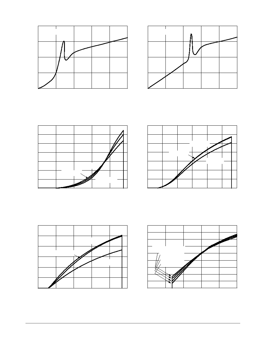
Figure 3. NCP304/5 Series 0.9 V
Detector Threshold Voltage vs. Temperature
Figure 4. NCP304/5 Series 2.7 V
Detector Threshold Voltage vs. Temperature
Figure 5. NCP304/5 Series 4.5 V
Detector Threshold Voltage vs. Temperature
V
in
, INPUT VOLTAGE (V)
0
0.2
0.4
0.6
0.8
1.0
0.8
0.6
0.4
0.2
0
1.0
Figure 6. NCP304L/5L Series 0.9 V
Reset Output Voltage vs. Input Voltage
0
1.0
1.5
2.0
2.5
3.0
2.0
1.5
1.0
0.5
0
3.0
V
in
, INPUT VOLTAGE (V)
0.5
2.5
Figure 7. NCP304L/5L Series 2.7 V
Reset Output Voltage vs. Input Voltage
0
1.0
2.0
3.0
4.0
5.0
4.0
3.0
2.0
1.0
0
5.0
6.0
7.0
6.0
V
in
, INPUT VOLTAGE (V)
Figure 8. NCP304L/5L Series 4.5 V
Reset Output Voltage vs. Input Voltage
V
OUT
, OUTPUT OUTPUT (V)
V
OUT
, OUTPUT OUTPUT (V)
V
DET
, DETECT
OR THRESHOLD VOL
T
AGE (V)
V
DET
, DETECT
OR THRESHOLD VOL
T
AGE (V)
V
DET
, DETECT
OR THRESHOLD VOL
T
AGE (V)
V
DET-
V
DET+
V
DET-
V
DET+
V
DET-
T
A
= -30∞C
T
A
= 25∞C
T
A
= 85∞C
T
A
= -30∞C
T
A
= 25∞C
T
A
= 85∞C
T
A
= -30∞C
T
A
= 25∞C
T
A
= 85∞C

NCP304, NCP305
http://onsemi.com
13
0
V
OUT
, OUTPUT VOLTAGE (V)
0.2
0.4
0.6
0.8
1.0
1.2
0.6
0.4
0
0.2
0.8
1.0
0
35
25
15
5.0
0.5
1.0
1.5
2.0
2.5
3.0
10
0
3.5
4.0
20
30
V
OUT
, OUTPUT VOLTAGE (V)
T
A
= 25∞C
T
A
= 25∞C
V
in
, INPUT VOLTAGE (V)
0
2.0
4.0
6.0
8.0
2.0
1.5
1.0
0.5
0
10
16
12
8.0
4.0
0
2.0
6.0
10
14
0
0.5
1.0
1.5
2.0
2.5
V
OUT
, OUTPUT VOLTAGE (V)
T
A
= 25∞C
V
in
= 2.0V
V
in
= 1.5 V
V
in
= 2.5 V
V
in
= 4.0 V
V
in
= 3.5 V
V
in
= 3.0 V
V
in
= 2.5 V
V
in
= 2.0 V
V
in
= 1.5 V
T
A
= 25∞C
I
OUT
, OUTPUT SINK CURRENT (mA)
I
OUT
, OUTPUT SINK CURRENT (mA)
I
OUT
, OUTPUT SINK CURRENT (mA)
I
in
, INPUT CURRENT (
m
A)
1.5
V
OUT
, OUTPUT VOLTAGE (V)
I
OUT
, OUTPUT SOURCE CURRENT (mA)
0
2.0
2.5
1.5
1.0
0.5
0.5
1.0
0
2.0
2.5
V
in
= 2.5 V
V
in
= 2.0 V
V
in
= 1.5 V
0
3.0
2.5
2.0
1.5
2.0
1.5
1.0
1.0
0.5
0
0.5
2.5
3.0
V
in
, INPUT VOLTAGE (V)
V
OUT
, OUTPUT VOL
T
AGE (V)
T
A
= -30∞C
T
A
= 25∞C
T
A
= 85∞C
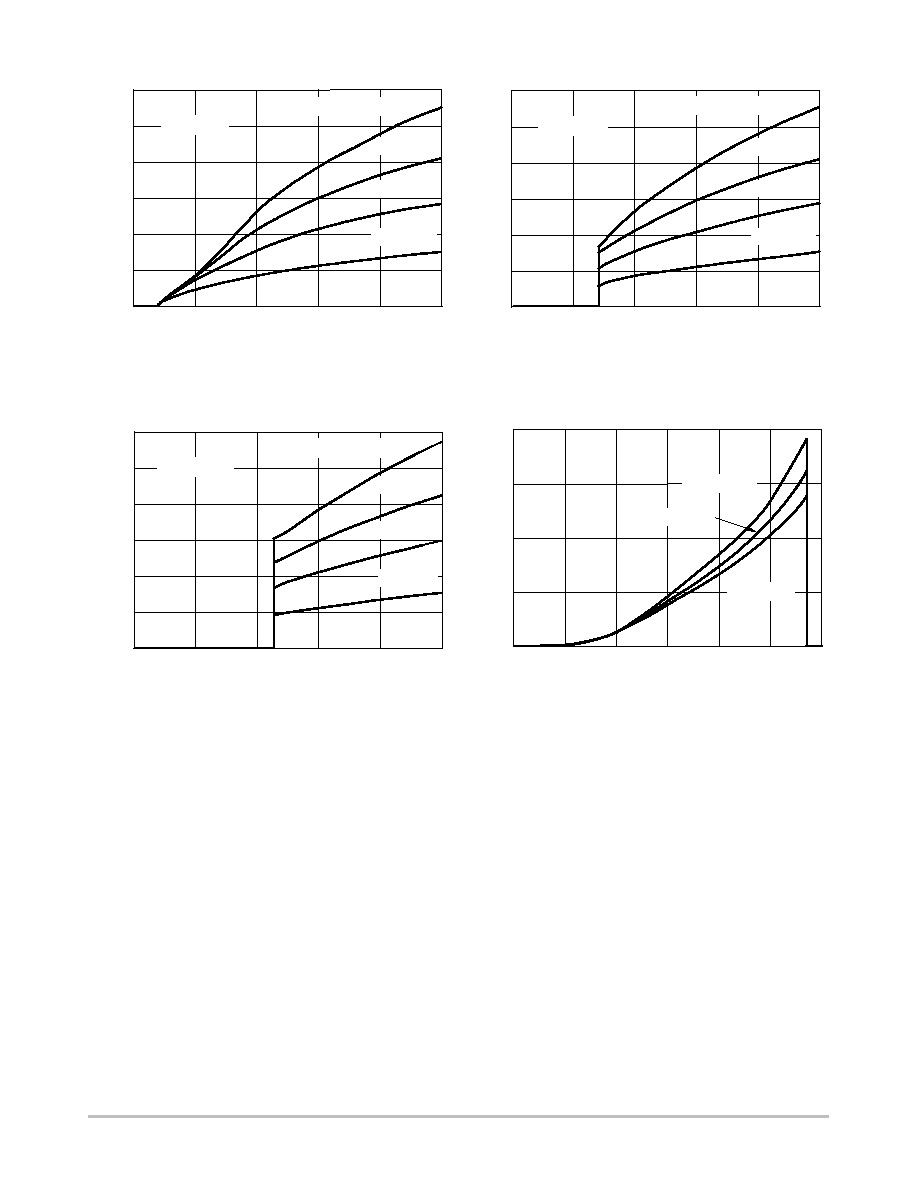
Figure 9. NCP304H/5H Series 2.7 V
Reset Output Voltage vs. Input Voltage
Figure 10. NCP304H/5L Series 0.9 V
Reset Output Sink Current vs. Output Voltage
Figure 11. NCP304H/5L Series 2.7 V
Reset Output Sink Current vs. Output Voltage
Figure 12. NCP304H/5L Series 4.5 V
Reset Output Sink Current vs. Output Voltage
Figure 13. NCP304H Series 2.7 V Reset Output
Source Current vs. Output Voltage
Figure 14. NCP304/5 Series 0.9 V
Input Current vs. Input Voltage
V
in
= 0.7 V
V
in
= 0.85 V
NCP304, NCP305
http://onsemi.com
14
60
20
80
10
40
0
90
V
in
, INPUT VOLTAGE (V)
I
OUT
, OUTPUT SINK CURRENT (mA)
0
8.0
6.0
4.0
2.0
10
V
out
= V
in
- 2.1 V
70
50
30
= V
in
- 1.5 V
= V
in
- 1.0 V
= V
in
- 0.5 V
V
in
, INPUT VOLTAGE (V)
1.2
0.8
0.4
0
0.2
0.6
1.0
1.4
0
0.2
0.4
0.6
0.8
1.0
V
in
, INPUT VOLTAGE (V)
0
7.0
5.0
3.0
1.0
0.5
1.0
1.5
2.0
2.5
3.0
2.0
0
4.0
6.0
V
in
, INPUT VOLTAGE (V)
0
1.0
2.0
3.0
4.0
5.0
12
6.0
4.0
0
2.0
8.0
10
I
OUT
, OUTPUT SINK CURRENT (mA)
I
OUT
, OUTPUT SINK CURRENT (mA)
I
OUT
, OUTPUT SINK CURRENT (mA)
T
A
= 85∞C
T
A
= 25∞C
T
A
= -30∞C
T
A
= -30∞C
T
A
= 85∞C
T
A
= 25∞C
T
A
= 25∞C
T
A
= -30∞C
T
A
= 85∞C
2.0
0
2.0
6.0
8.0
10
0.5
0
V
in
, INPUT VOLTAGE (V)
4.0
1.0
0
2.0
6.0
8.0
1.5
1.0
0.5
0
V
in
, INPUT VOLTAGE (V)
4.0
10
1.5
2
I
in
, INPUT CURRENT (
m
A)
I
in
, INPUT CURRENT (
m
A)
Figure 15. NCP304/5 Series 2.7 V
Input Current vs. Input Voltage
Figure 16. NCP304/5 Series 4.5 V
Input Current vs. Input Voltage
Figure 17. NCP304H/5L Series 0.9 V
Reset Output Sink Current vs. Input Voltage
Figure 18. NCP304H/5L Series 2.7 V
Reset Output Sink Current vs. Input Voltage
Figure 19. NCP304H/5L Series 4.5 V
Reset Output Sink Current vs. Input Voltage
Figure 20. NCP304H/5H Series 2.7 V
Reset Output Sink Current vs. Input Voltage
T
A
= 25∞C
T
A
= 25∞C
NCP304, NCP305
http://onsemi.com
15
10
8.0
0
0
2.0
4.0
6.0
8.0
10
V
in
, INPUT VOLTAGE (V)
2.0
4.0
6.0
12
V
OUT
= V
in
-2.1 V
V
in
-1.5 V
V
in
-1.0 V
V
in
- 0.5 V
T
A
= 25∞C
I
OUT
, OUTPUT SOURCE CURRENT (mA)
0
2.0
2.0
3.0
2.5
1.5
1.0
V
in
, INPUT VOLTAGE (V)
I
OUT
, OUTPUT SOURCE CURRENT (mA)
1.0
0
0.5
4.0
3.0
T
A
= -30∞C
T
A
= 25∞C
T
A
= 85∞C
10
8.0
2.0
0
0
2.0
4.0
6.0
8.0
10
V
in
, INPUT VOLTAGE (V)
4.0
6.0
12
V
OUT
= V
in
-2.1 V
V
in
-1.5 V
V
in
-1.0 V
V
in
- 0.5 V
T
A
= 25∞C
10
8.0
0
0
2.0
4.0
6.0
8.0
10
V
in
, INPUT VOLTAGE (V)
2.0
4.0
6.0
12
V
OUT
= V
in
-2.1 V
V
in
-1.5 V
V
in
-1.0 V
V
in
- 0.5 V
T
A
= 25∞C
I
OUT
, OUTPUT SOURCE CURRENT (mA)
I
OUT
, OUTPUT SOURCE CURRENT (mA)
Figure 21. NCP304H Series 0.9 V
Reset Output Source Current vs. Input Voltage
Figure 22. NCP304H Series 2.7 V
Reset Output Source Current vs. Input Voltage
Figure 23. NCP304H Series 4.5 V
Reset Output Source Current vs. Input Voltage
Figure 24. NCP304H Series 2.7 V
Reset Output Source Current vs. Input Voltage

NCP304, NCP305
http://onsemi.com
16
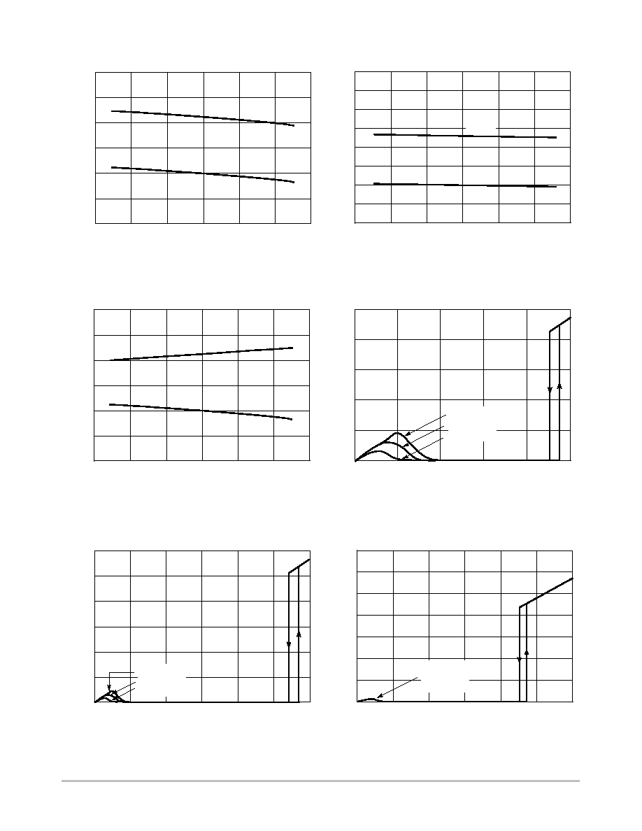
OPERATING DESCRIPTION
The NCP304 and NCP305 series devices are second
generation ultra-low current voltage detectors. Figures 25
and 26 show a timing diagram and a typical application.
Initially consider that input voltage V
in
is at a nominal level
and it is greater than the voltage detector upper threshold
(V
DET+
), and the reset output (Pin 1) will be in the high state
for active low devices, or in the low state for active high
devices. If there is a power interruption and V
in
becomes
significantly deficient, it will fall below the lower detector
threshold (V
DET-
). This sequence of events causes the Reset
output to be in the low state for active low devices, or in the
high state for active high devices. After completion of the
power interruption, V
in
will again return to its nominal level
and become greater than the V
DET+
. The voltage detector
has built-in hysteresis to prevent erratic reset operation as
the comparator threshold is crossed.
Although these device series are specifically designed for
use as reset controllers in portable microprocessor based
systems, they offer a cost-effective solution in numerous
applications where precise voltage monitoring is required.
Figure 26 through Figure 32 shows various application
examples.
Figure 25. Timing Waveforms
V
in
V
DET
+
V
DET-
Input Voltage, Pin 2
V
in
0 V
Reset Output (Active Low), Pin 1
Reset Output (Active High), Pin 1
V
in
0 V
V
DET
+
V
DET-
V
DET
+
V
DET-
NCP304, NCP305
http://onsemi.com
17
APPLICATION CIRCUIT INFORMATION
Figure 26. Microprocessor Reset Circuit
2 Input
1
Reset Output
GN
D
NCP304
LSQ27T1
Figure 27. Battery Charge Indicator
2 Input
1
Reset Output
GN
D
GND
V
DD
Reset
V
DD
NCP304
Series
3
3
Microprocessor
*
Required for
NCP305
V
in
< 2.7 ON
V
in
> 2.835 ON
To Additional Circuitry
*
2.85 V
2.70 V
Low state output if either
power supply is below the
respective undervoltage de-
tector threshold but greater
than 1.0 V.
2
1
NCP305
LSQ45T1
Figure 28. Dual Power Supply Undervoltage Supervision
3
V
supply
2
1
NCP305
LSQ30T1
3
3.3 V
5.0 V
GN
D
Input
Reset Output
GN
D
Input
Reset Output

NCP304, NCP305
http://onsemi.com
18
Figure 29. Microprocessor Reset Circuit with Additional Hysteresis
2
1
NCP301
LSN27T1
3
V
DD
GN
D
Reset Output
Input
R
H
R
L
NCP301
LSN27T1
GN
D
NCP305
LSQ27T1
GN
D
GN
D
Reset
V
DD
Microprocessor
Comparator hysteresis can be increased with the addition of
resistor R
H
. The hysteresis equations have been simplified and
do not account for the change of input current I
in
as V
in
crosses
the comparator threshold. The internal resistance, R
in
is simply
calculated using I
in
= 0.26 mA at 2.6 V.
V
in
Decreasing:
V
th
+
R
H
R
in
) 1 V
DET*
V
in
Increasing:
V
th
+
R
H
R
in
¯ R
L
) 1 V
DET*
) V
HYS
V
HYS
= V
in
Increasing - V
in
Decreasing
Test Data
V
th
Decreasing
(mV)
V
th
Increasing
(mV)
V
HYS
(mV)
R
H
(W)
R
L
(kW)
¡¡¡¡¡¡
¡¡¡¡¡¡
¡ ¡¡¡¡¡
¡ ¡¡¡¡¡
¡ ¡¡¡¡¡
¡ ¡¡¡¡¡
¡ ¡¡¡¡¡
¡¡¡¡¡¡
2.70
2.70
2.70
2.70
2.70
2.70
2.70
2.70
2.70
2.70
¡¡¡¡¡¡
¡¡¡¡¡¡
¡ ¡¡¡¡¡
¡ ¡¡¡¡¡
¡ ¡¡¡¡¡
¡ ¡¡¡¡¡
¡ ¡¡¡¡¡
¡¡¡¡¡¡
2.84
2.87
2.88
2.91
2.90
2.94
2.98
2.70
3.04
3.15
¡¡¡
¡¡¡
¡¡¡
¡¡¡
¡¡¡
¡¡¡
¡¡¡
¡¡¡
0.135
0.17
0.19
0.21
0.20
0.24
0.28
0.27
0.34
0.35
¡¡¡
¡¡¡
¡¡¡
¡¡¡
¡¡¡
¡¡¡
¡¡¡
¡¡¡
0
100
100
100
220
220
220
470
470
470
¡¡
¡¡
¡¡
¡¡
¡¡
¡¡
¡¡
¡¡
-
10
6.8
4.3
10
6.8
4.3
10
6.8
4.3
Figure 30. Simple Clock Oscillator
NCP301
LSN27T1
GN
D
Reset Output
Input
82 k
NCP301
LSN27T1
GN
D
NCP302
HSQ27T1
C
5.0 V
100 k
C (mF)
f
OSC
(kHz)
I
Q
(mA)
0.01
2590
21.77
0.1
490
21.97
1.0
52
22.07
Test Data
2
3
1

NCP304, NCP305
http://onsemi.com
19
Figure 31. Microcontroller Systems Load Sensing
NCP301
LSN27T1
50 k
NCP301
LSN27T1
NCP305
LSQ09T1
V
supply
Load
R
sense
Input
2
3
GND
1
Reset Output
Microcontroller
GND
V
DD
If:
I
Load
t
V
DET -
/R
sense
I
Load
w (V
DET -
+V
HYS
)/R
sense
Then:
Reset Output = 0 V
Reset Output = V
DD
This circuit monitors the current at the load. As
current flows through the load, a voltage drop with
respect to ground appears across R
sense
where
V
sense
= I
load
* R
sense.
The following conditions apply:
Figure 32. LED Bar Graph
NCP301
LSN27T1
2
NCP301
LSN27T1
NCP305
LSQ45T1
3
1
V
supply
NCP301
LSN27T1
2
NCP301
LSN27T1
NCP305
LSQ27T1
3
1
NCP301
LSN27T1
2
NCP301
LSN27T1
NCP305
LSQ18T1
3
1
Input
GND
Reset
Output
Input
GND
Reset
Output
Input
GND
Reset
Output
V
in
= 1.0 V to 10 V
A simple voltage monitor can be constructed by connecting several voltage detectors as shown above. Each LED will
sequentially turn on when the respective voltage detector threshold (V
DET-
+V
HYS
) is exceeded. Note that detector
thresholds (V
DET-
) that range from 0.9 V to 4.9 V in 100 mV steps can be manufactured.

NCP304, NCP305
http://onsemi.com
20
ORDERING INFORMATION
Device
Threshold
Voltage
Output
Type
Reset
Marking
Package
Shipping
NCP304LSQ09T1
0.9
SHG
SC-82AB
NCP304LSQ09T1G
0.9
SHGG
SC-82AB
(Pb-Free)
NCP304LSQ18T1
1.8
SGX
SC-82AB
NCP304LSQ20T1
2.0
SGV
SC-82AB
NCP304LSQ23T1
2.3
SGR
SC-82AB
NCP304LSQ25T1
2.5
SGP
SC-82AB
NCP304LSQ25T1G
2.5
SGPG
SC-82AB
(Pb-Free)
NCP304LSQ27T1
2.7
SGN
SC-82AB
NCP304LSQ29T1
2.9
SGK
SC-82AB
NCP304LSQ29T1G
2.9
SGKG
SC-82AB
(Pb-Free)
NCP304LSQ30T1
3.0
SGJ
SC-82AB
NCP304LSQ30T1G
3.0
CMOS
Active
Low
SGJG
SC-82AB
(Pb-Free)
NCP304LSQ33T1
3.3
CMOS
Low
SGG
SC-82AB
NCP304LSQ37T1
3.7
SGB
SC-82AB
NCP304LSQ38T1
3.8
SGA
SC-82AB
NCP304LSQ40T1
4.0
SFY
SC-82AB
NCP304LSQ42T1
4.2
SFU
SC-82AB
3000 / Tape & Reel
NCP304LSQ43T1
4.3
SFV
SC-82AB
NCP304LSQ43T1G
4.3
SFV
G
SC-82AB
(Pb-Free)
NCP304LSQ45T1
4.5
SFS
SC-82AB
NCP304LSQ45T1G
4.5
SFSG
SC-82AB
(Pb-Free)
NCP304LSQ46T1
4.6
SFR
SC-82AB
NCP304LSQ47T1
4.7
SFQ
SC-82AB
NCP304LSQ47T1G
4.7
SFQG
SC-82AB
(Pb-Free)
NCP304HSQ09T1
0.9
SNQ
SC-82AB
NCP304HSQ18T1
1.8
SNZ
SC-82AB
NCP304HSQ20T1
2.0
SOB
SC-82AB
NCP304HSQ20T1G
2.0
CMOS
Active
SOBG
SC-82AB
(Pb-Free)
NCP304HSQ22T1
2.2
CMOS
Active
High
SOD
SC-82AB
NCP304HSQ27T1
2.7
SOI
SC-82AB
NCP304HSQ29T1
2.9
SOK
SC-82AB
NCP304HSQ29T1G
2.9
SOKG
SC-82AB
(Pb-Free)
NOTE: The ordering information lists standard undervoltage thresholds with active low outputs. Additional active low threshold devices, ranging
from 0.9 V to 4.9 V in 100 mV increments and NCP304 active high output devices, ranging from 0.9 V to 4.9 V in 100 mV increments
can be manufactured. Contact your ON Semiconductor representative for availability. The electrical characteristics of these additional
devices are shown in Tables 1 and 2.
For information on tape and reel specifications, including part orientation and tape sizes, please refer to our Tape and Reel Packaging Specifi-
cations Brochure, BRD8011/D.

NCP304, NCP305
http://onsemi.com
21
ORDERING INFORMATION
Device
Threshold
Voltage
Output
Type
Reset
Marking
Package
Shipping
NCP304HSQ30T1
3.0
SOL
SC-82AB
NCP304HSQ30T1G
3.0
SOLG
SC-82AB
(Pb-Free)
NCP304HSQ45T1
4.5
Active
SPA
SC-82AB
NCP304HSQ45T1G
4.5
CMOS
Active
High
SPAG
SC-82AB
(Pb-Free)
3000 / Tape & Reel
NCP304HSQ47T1
4.7
SPC
SC-82AB
NCP304HSQ47T1G
4.7
SPCG
SC-82AB
(Pb-Free)
NCP305LSQ09T1
0.9
SIZ
SC-82AB
NCP305LSQ09T1G
0.9
SIZG
SC-82AB
(Pb-Free)
NCP305LSQ11T1
1.1
SIX
SC-82AB
NCP305LSQ11T1G
1.1
SIXG
SC-82AB
(Pb-Free)
NCP305LSQ15T1
1.5
SIS
SC-82AB
NCP305LSQ16T1
1.6
SIR
SC-82AB
NCP305LSQ16T1G
1.6
SIRG
SC-82AB
(Pb-Free)
NCP305LSQ17T1
1.7
SIQ
SC-82AB
NCP305LSQ17T1G
1.7
SIQG
SC-82AB
(Pb-Free)
NCP305LSQ18T1
1.8
SIP
SC-82AB
NCP305LSQ20T1
2.0
SIN
SC-82AB
NCP305LSQ22T1
2.2
SIK
SC-82AB
NCP305LSQ22T1G
2.2
Open
Drain
Active
Low
SIKG
SC-82AB
(Pb-Free)
3000 / Tape & Reel
NCP305LSQ23T1
2.3
SIJ
SC-82AB
NCP305LSQ24T1
2.4
SII
SC-82AB
NCP305LSQ25T1
2.5
SIH
SC-82AB
NCP305LSQ27T1
2.7
SIF
SC-82AB
NCP305LSQ27T1G
2.7
SIFG
SC-82AB
(Pb-Free)
NCP305LSQ28T1
2.8
SIE
SC-82AB
NCP305LSQ28T1G
2.8
SIEG
SC-82AB
(Pb-Free)
NCP305LSQ29T1
2.9
SID
SC-82AB
NCP305LSQ29T1G
2.9
SIDG
SC-82AB
(Pb-Free)
NCP305LSQ30T1
3.0
SIC
SC-82AB
NCP305LSQ30T1G
3.0
SICG
SC-82AB
(Pb-Free)
NCP305LSQ30T3
3.0
SIC
SC-82AB
10000 / Tape & Reel
NOTE: The ordering information lists standard undervoltage thresholds with active low outputs. Additional active low threshold devices, ranging
from 0.9 V to 4.9 V in 100 mV increments and NCP304 active high output devices, ranging from 0.9 V to 4.9 V in 100 mV increments
can be manufactured. Contact your ON Semiconductor representative for availability. The electrical characteristics of these additional
devices are shown in Tables 1 and 2.
For information on tape and reel specifications, including part orientation and tape sizes, please refer to our Tape and Reel Packaging Specifi-
cations Brochure, BRD8011/D.
NCP304, NCP305
http://onsemi.com
22
ORDERING INFORMATION
Device
Shipping
Package
Marking
Reset
Output
Type
Threshold
Voltage
NCP305LSQ31T1
3.1
SIB
SC-82AB
NCP305LSQ32T1
3.2
SIA
SC-82AB
NCP305LSQ33T1
3.3
SHZ
SC-82AB
NCP305LSQ34T1
3.4
SHY
SC-82AB
NCP305LSQ35T1
3.5
SHX
SC-82AB
NCP305LSQ35T1G
3.5
SHXG
SC-82AB
(Pb-Free)
NCP305LSQ36T1
3.6
SHU
SC-82AB
NCP305LSQ36T1G
3.6
SHUG
SC-82AB
(Pb-Free)
NCP305LSQ37T1
3.7
Open
Drain
Active
Lo
SHV
SC-82AB
3000 / Tape & Reel
NCP305LSQ37T1G
3.7
p
Drain
Low
SHVG
SC-82AB
(Pb-Free)
3000 / Tape & Reel
NCP305LSQ40T1
4.0
SHR
SC-82AB
NCP305LSQ44T1
4.4
SHN
SC-82AB
NCP305LSQ45T1
4.5
SHL
SC-82AB
NCP305LSQ45T1G
4.5
SHLG
SC-82AB
(Pb-Free)
NCP305LSQ47T1
4.7
SHJ
SC-82AB
NCP305LSQ49T1
4.9
SHH
SC-82AB
NCP305LSQ49T1G
4.9
SHHG
SC-82AB
(Pb-Free)
NOTE: The ordering information lists standard undervoltage thresholds with active low outputs. Additional active low threshold devices, ranging
from 0.9 V to 4.9 V in 100 mV increments and NCP304 active high output devices, ranging from 0.9 V to 4.9 V in 100 mV increments
can be manufactured. Contact your ON Semiconductor representative for availability. The electrical characteristics of these additional
devices are shown in Tables 1 and 2.
For information on tape and reel specifications, including part orientation and tape sizes, please refer to our Tape and Reel Packaging Specifi-
cations Brochure, BRD8011/D.
NCP304, NCP305
http://onsemi.com
23
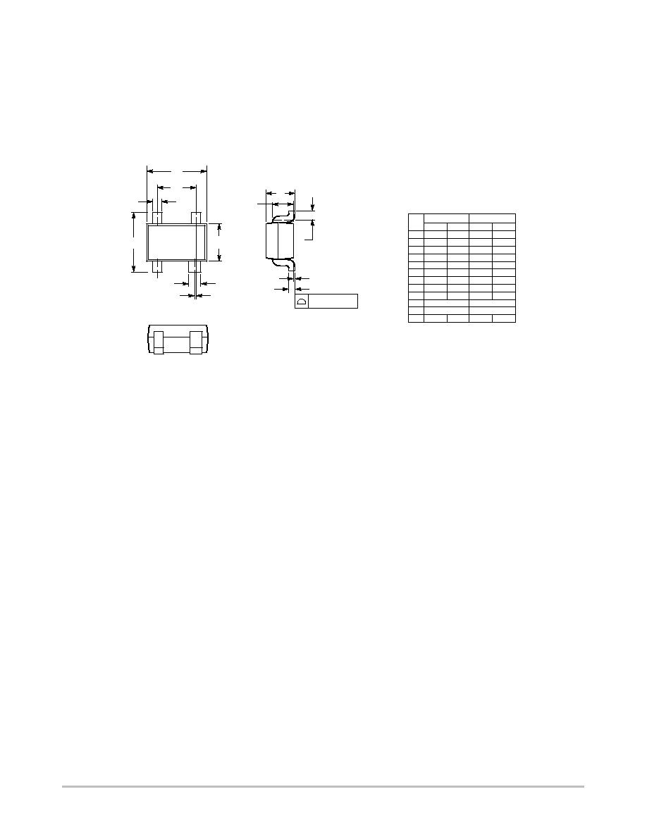
PACKAGE DIMENSIONS
SC-82AB
SQ SUFFIX
CASE 419C-02
ISSUE C
NOTES:
1. DIMENSIONING AND TOLERANCING PER
ANSI Y14.5M, 1982.
2. CONTROLLING DIMENSION: MILLIMETER.
3. 419C-01 OBSOLETE. NEW STANDARD IS
419C-02.
4. DIMENSIONS A AND B DO NOT INCLUDE
MOLD FLASH, PROTRUSIONS, OR GATE
BURRS.
1
2
3
A
G
S
N
J
K
4
D
3 PL
B
F
L
C
H
0.05 (0.002)
DIM
MIN
MAX
MIN
MAX
INCHES
MILLIMETERS
A
1.8
2.2
0.071
0.087
B
1.15
1.35
0.045
0.053
C
0.8
1.1
0.031
0.043
D
0.2
0.4
0.008
0.016
F
0.3
0.5
0.012
0.020
G
1.1
1.5
0.043
0.059
H
0.0
0.1
0.000
0.004
J
0.10
0.26
0.004
0.010
K
0.1
---
0.004
---
L
0.05 BSC
0.002 BSC
N
0.2 REF
0.008 REF
S
1.8
2.4
0.07
0.09

NCP304, NCP305
http://onsemi.com
24
ON Semiconductor and are registered trademarks of Semiconductor Components Industries, LLC (SCILLC). SCILLC reserves the right to make changes without further notice
to any products herein. SCILLC makes no warranty, representation or guarantee regarding the suitability of its products for any particular purpose, nor does SCILLC assume any liability
arising out of the application or use of any product or circuit, and specifically disclaims any and all liability, including without limitation special, consequential or incidental damages.
"Typical" parameters which may be provided in SCILLC data sheets and/or specifications can and do vary in different applications and actual performance may vary over time. All
operating parameters, including "Typicals" must be validated for each customer application by customer's technical experts. SCILLC does not convey any license under its patent rights
nor the rights of others. SCILLC products are not designed, intended, or authorized for use as components in systems intended for surgical implant into the body, or other applications
intended to support or sustain life, or for any other application in which the failure of the SCILLC product could create a situation where personal injury or death may occur. Should
Buyer purchase or use SCILLC products for any such unintended or unauthorized application, Buyer shall indemnify and hold SCILLC and its officers, employees, subsidiaries, affiliates,
and distributors harmless against all claims, costs, damages, and expenses, and reasonable attorney fees arising out of, directly or indirectly, any claim of personal injury or death
associated with such unintended or unauthorized use, even if such claim alleges that SCILLC was negligent regarding the design or manufacture of the part. SCILLC is an Equal
Opportunity/Affirmative Action Employer. This literature is subject to all applicable copyright laws and is not for resale in any manner.
PUBLICATION ORDERING INFORMATION
N. American Technical Support: 800-282-9855 Toll Free
USA/Canada
Japan: ON Semiconductor, Japan Customer Focus Center
2-9-1 Kamimeguro, Meguro-ku, Tokyo, Japan 153-0051
Phone: 81-3-5773-3850
NCP304/D
LITERATURE FULFILLMENT:
Literature Distribution Center for ON Semiconductor
P.O. Box 61312, Phoenix, Arizona 85082-1312 USA
Phone: 480-829-7710 or 800-344-3860 Toll Free USA/Canada
Fax: 480-829-7709 or 800-344-3867 Toll Free USA/Canada
Email: orderlit@onsemi.com
ON Semiconductor Website: http://onsemi.com
Order Literature: http://www.onsemi.com/litorder
For additional information, please contact your
local Sales Representative.