
©
Semiconductor Components Industries, LLC, 2006
May, 2006 - Rev. 1
1
Publication Order Number:
NCP3163/D
NCP3163
3.4 A, Step-Up/Down/
Inverting 50-300 kHz
Switching Regulator
The NCP3163 Series is a performance enhancement to the popular
MC33163 and MC34163 monolithic DC-DC converters. These
devices consist of an internal temperature compensated reference,
comparator, controlled duty cycle oscillator with an active current
limit circuit, driver and high current output switch. This controller was
specifically designed to be incorporated in step-down, step-up, or
voltage-inverting applications with a minimum number of external
components. The NCP3163 comes in an exposed pad package which
can greatly increase the power dissipation of the built in power switch.
Features
∑
Output Switch Current in Excess of 3.0 A
∑
3.4 A Peak Switch Current
∑
Frequency is Adjustable from 50 kHz to 300 kHz
∑
Operation from 2.5 V to 40 V Input
∑
Externally Adjustable Operating Frequency
∑
Precision 2% Reference for Accurate Output Voltage Control
∑
Driver with Bootstrap Capability for Increased Efficiency
∑
Cycle-by-Cycle Current Limiting
∑
Internal Thermal Shutdown Protection
∑
Low Voltage Indicator Output for Direct Microprocessor Interface
∑
Exposed Pad Power Package
∑
Low Standby Current
∑
This is a Pb-Free Device
+
16
9
10
11
12
13
14
15
8
7
6
5
4
3
2
LVI
Oscillator
+
+
-
Current
Limit
Figure 1. Typical Buck Application Circuit
(Bottom View)
-
+
+
+
-
1
V
CC
V
CC
V
CC
V
in
C
in
Thermal
V
out
+
C
O
R
S
Q
See detailed ordering and shipping information in the package
dimensions section on page 18 of this data sheet.
ORDERING INFORMATION
MARKING
DIAGRAMS
NCP3163x = Specific Device Code
A
= Assembly Location
WL = Wafer Lot
YY = Year
WW = Work Week
G
= Pb-Free Package
G
= Pb-Free Package
1
16
SOIC-16W
EXPOSED PAD
PW SUFFIX
CASE 751AG
http://onsemi.com
16
1
NCP3163xPW
AWLYYWWG
*For additional information on our Pb-Free strategy
and soldering details, please download the
ON Semiconductor Soldering and Mounting
Techniques Reference Manual, SOLDERRM/D.
18-LEAD DFN
MN SUFFIX
CASE 505
1
NCP3163x
AWLYYWW
G
G
1
18
18
(Note: Microdot may be in either location)

NCP3163
http://onsemi.com
2
16
9
10
11
12
13
14
15
8
7
6
5
4
3
2
LVI
Oscillator
+
+
-
Current
Limit
Figure 2. Representative Block Diagram
(Bottom View)
-
+
+
+
-
1
V
CC
V
CC
V
CC
Thermal
R
S
Q
Driver Collector
Switch Collector
0.25 V
Switch Emitter
Bootstrap Input
Voltage Feedback 1
Voltage Feedback 2
LVI Output
Gnd
I
PKsense
V
CC
R
SC
Timing Capacitor
2.0 mA
7.0 V
60
Q1
Q2
1.125 V
15 k
1.25 V
Feedback
Comparator
Shutdown
C
T
R
DT
45 k
Latch
+
-
= Sink Only
Positive True Logic
PIN FUNCTION DESCRIPTION
SOIC16
DFN18
PIN NAME
DESCRIPTION
1
15
LVI Output
This pin will sink current when FB1 and FB2 are less than the LVI threshold (V
th
).
2
16
Voltage Feedback 2
Connecting this pin to a resistor divider off of the output will regulate the application
according to the V
out
design equation in Figure 22.
3
17
Voltage Feedback 1
Connecting this pin directly to the output will regulate the device to 5.05 V.
4
18
GND
Ground pin for all internal circuits and power switch.
6
1
Timing Capacitor
Connect a capacitor to this pin to set the frequency. The addition of a parallel resis-
tor will decrease the maximum duty cycle and increase the frequency.
7
3
V
CC
Power pin for the IC.
8
4
I
pk
Sense
When (V
CC
-V
IPKsense
) > 250 mV the circuit resets the output driver on a pulse by
pulse basis.
9
5
Drive Collector
Voltage driver collector
10,11
6,7,8,9
Switch Collector
Internal switch transistor collector
14,15
10,11,12,13
Switch Emitter
Internal switch transistor emitter
16
14
Bootstrap Input
Connect this pin to V
CC
for operation at low V
CC
levels. For some topologies, a
series resistor and capacitor can be utilized to improve the converter efficiency.
5,12,13
2
No Connect
These pins have no connection.
Exposed
Pad
Exposed
Pad
Exposed Pad
The exposed pad beneath the package must be connected to GND (pin 4). Addi-
tionally, using proper layout techniques, the exposed pad can greatly enhance the
power dissipation capabilities of the NCP3163.

NCP3163
http://onsemi.com
3
MAXIMUM RATINGS
(Note 1)
Rating
Symbol
Value
Unit
Power Supply Voltage
V
CC
0 to +40
V
Switch Collector Voltage Range
V
CSW
-1.0 to +40
V
Switch Emitter Voltage Range
V
ESW
-2.0 to +40
V
Switch Collector to Emitter Voltage
V
CESW
+40
V
Switch Current
I
SW
3.4
A
Driver Collector Voltage (Pin 8)
V
CC
-1.0 to +40
V
Driver Collector Current (Pin 8)
I
CC
150
mA
Bootstrap Input Current Range
I
BST
-100 to +100
mA
Current Sense Input Voltage Range
V
IPKSNS
(V
CC
- 7.0) to (V
CC
+ 1.0)
V
Feedback and Timing Capacitor Input Voltage Range
V
in
-1.0 to +7.0
V
Low Voltage Indicator Output Voltage Range
V
CLVI
-1.0 to +40
V
Low Voltage Indicator Output Sink Current
I
CLVI
10
mA
Power Dissipation and Thermal Characteristics
Thermal Characteristics
Thermal Resistance, Junction-to-Case
Thermal Resistance, Junction-to-Air
R
q
JC
R
q
JA
15
56
∞
C/W
Storage Temperature Range
T
stg
-65 to +150
∞
C
Maximum Junction Temperature
T
Jmax
+150
∞
C
Operating Ambient Temperature (Note 3)
NCP3163PW
NCP3163BPW
T
A
0 to +70
-40 to +85
∞
C
PIN CONNECTIONS
N/C
GND
Voltage Feedback 1
LVI Output
Bootstrap Input
Switch Emitter
Switch Emitter
Switch Emitter
Switch Emitter
Voltage Feedback 2
Timing Capacitor
N/C
V
CC
I
pk
Sense
Switch Collector
Switch Collector
Switch Collector
Switch Collector
Driver Collector
1
2
3
4
5
6
7
8
16
15
14
13
12
11
10
9
17
18
Note: Pin 18 must be tied to EP Flag on PCB
GND
EP Flag
Maximum ratings are those values beyond which device damage can occur. Maximum ratings applied to the device are individual stress limit
values (not normal operating conditions) and are not valid simultaneously. If these limits are exceeded, device functional operation is not implied,
damage may occur and reliability may be affected.
1. This device series contains ESD protection and exceeds the following tests:
Human Body Model 1500 V per MIL-STD-883, Method 3015.
Machine Model Method 150 V.
2. This device contains latch-up protection and exceeds 100 mA per JEDEC Standard JESD78.
3. Maximum package power dissipation limits must be observed. Maximum Junction Temperature must not be exceeded.
4. The pins which are not defined may not be loaded by external signals.
1
16
15
14
13
12
11
10
9
2
3
4
5
6
7
8
(Top View)
LVI Output
Voltage Feedback 2
Voltage Feedback 1
GND
Timing Capacitor
V
CC
I
pk
Sense
Bootstrap Input
Switch
Emitter
N/C
Switch Collector
Driver Collector
NCP3163
http://onsemi.com
4
ELECTRICAL CHARACTERISTICS
(V
CC
= 15 V, Pin 16 = V
CC
, C
T
= 270 pF, R
T
= 15 k
W
, for typical values T
A
= 25
∞
C, for min/max
values T
A
is the operating ambient temperature range that applies (Note 5), unless otherwise noted.)
Characteristic
Symbol
Min
Typ
Max
Unit
OSCILLATOR
Frequency
T
A
= 25
∞
C, V
CC
= 15 V
Total Variation over V
CC
= 2.5 V to 40 V and Temperature (Note 5)
f
OSC
225
212
250
250
275
288
kHz
Charge Current
I
chg
-
225
-
m
A
Discharge Current
I
dischg
-
25
-
m
A
Charge to Discharge Current Ratio
I
chg
/I
dischg
8.0
9.0
10
-
Sawtooth Peak Voltage
V
OSC(P)
-
1.25
-
V
Sawtooth Valley Voltage
V
OSC(V)
-
0.55
-
V
FEEDBACK COMPARATOR 1
Threshold Voltage
T
A
= 25
∞
C
Total Variation over V
CC
= 2.5 V to 40 V and Temperature (Note 5)
V
th(FB1)
4.9
4.85
5.05
-
5.2
5.25
V
Threshold Voltage
Line Regulation (V
CC
= 2.5 V to 40 V, T
A
= 25
∞
C)
REGline
(FB1)
-
0.008
0.03
%/V
Input Bias Current (V
FB1
= 5.05 V)
I
IB(FB1)
-
100
200
m
A
FEEDBACK COMPARATOR 2
Threshold Voltage
T
A
= 25
∞
C, V
CC
= 15 V
Total Variation over V
CC
= 2.5 V to 40 V and Temperature (Note 5)
V
th(FB2)
1.225
1.213
1.25
-
1.275
1.287
V
Threshold Voltage
Line Regulation (V
CC
= 2.5 V to 40 V, T
A
= 25
∞
C)
REGline
(FB1)
-
0.008
0.03
%/V
Input Bias Current (V
FB2
= 1.25 V)
I
IB(FB2)
- 0.4
-
0.4
m
A
CURRENT LIMIT COMPARATOR
Threshold Voltage
T
A
= 25
∞
C
Total Variation over V
CC
= 2.5 V to 40 V, and Temperature (Note 5)
V
th(Sense)
-
230
250
-
-
270
mV
Input Bias Current (V
Ipk (Sense)
= 15 V)
I
IB(Sense)
-
1.0
20
m
A
DRIVER AND OUTPUT SWITCH (Note 6)
Saturation Voltage (I
SW
= 2.5 A, Pins 14, 15 grounded)
Non-Darlington Connection (R
Pin 9
= 110
W
to V
CC
, I
SW
/I
DRV
20)
Darlington Connection (Pins 9, 10, 11 connected) (Note 7)
V
CE(sat)
-
-
0.6
1.0
1.0
1.4
V
Collector Off-State Leakage Current (V
CE
= 40 V)
I
C(off)
-
0.02
100
m
A
Bootstrap Input Current Source (V
BS
= V
CC
+ 5.0 V)
I
source(DRV)
0.5
2.0
4.0
mA
Bootstrap Input Zener Clamp Voltage (I
Z
= 25 mA)
V
Z
V
CC
+ 6.0
V
CC
+ 7.0
V
CC
+ 9.0
V
LOW VOLTAGE INDICATOR
Input Threshold (V
FB2
Increasing)
V
th
1.07
1.125
1.18
V
Input Hysteresis (V
FB2
Decreasing)
V
H
-
15
-
mV
Output Sink Saturation Voltage (I
sink
= 2.0 mA)
V
OL(LVI)
-
0.15
0.4
V
Output Off-State Leakage Current (V
OH
= 15 V)
I
OH
-
0.01
5.0
m
A
TOTAL DEVICE
Standby Supply Current (V
CC
= 2.5 V to 40 V, Pin 8 = V
CC
,
Pins 6, 14, 15 = GND, remaining pins open)
I
CC
-
6.0
10
mA
5. Maximum package power dissipation limits must be observed.
6. Low duty cycle pulse techniques are used during test to maintain junction temperature as close to ambient as possible.
7. T
low
= 0
∞
C for NCP3163
T
high
= + 70
∞
C for NCP3163
= - 40
∞
C for NCP3163B
= + 85
∞
C for NCP3163B

NCP3163
http://onsemi.com
5
Figure 3. Oscillator Frequency vs. Timer
Capacitance (C
T
)
300
0
C
T
, TIMER CAPACITANCE (pF)
FREQUENCY
(kHz)
200
100
50
100
200
300
400
500
600
700
V
CC
= 15 V
T
A
= 25
∞C
Figure 4. Oscillator Frequency Change vs.
Temperature when only C
T
is connected to Pin 6
2.0
- 55
T
A
, AMBIENT TEMPERATURE (
∞C)
f OSC
,
OSCILLA
T
OR
FREQUENCY
CHANGE (%)
0
- 2.0
- 4.0
- 6.0
- 25
0
25
50
75
100
125
V
CC
= 15 V
C
T
= 620 pF
Figure 5. Oscillator Frequency Change vs.
Temperature when C
T
and R
T
are connected to Pin 6
4.0
- 50
TEMPERATURE (
∞C)
f OSC
,
OSCILLA
T
OR
FREQUENCY
CHANGE (%)
0
- 2.0
- 8.0
- 10
- 25
0
25
50
75
100
125
- 6.0
- 4.0
2.0
V
CC
= 15 V
C
T
= 230 pF
R
T
= 20 k
W
150
250
R
t
= 15 k
W
R
t
= open
Figure 6. Feedback Comparator 1 Input Bias
Current vs. Temperature
Figure 7. Feedback Comparator 2 Threshold
Voltage vs. Temperature
I IB
,
INPUT
BIAS CURRENT
(A)
140
- 55
T
A
, AMBIENT TEMPERATURE (
∞C)
120
100
80
60
- 25
0
25
50
75
100
125
V
th(FB2)
, COMP
ARA
T
OR
2
THRESHOLD
VOL
T
AGE (mV)
1300
1280
1260
1240
1220
1200
- 55
T
A
, AMBIENT TEMPERATURE (
∞C)
- 25
0
25
50
75
100
125
V
th
Typ = 1250 mV
V
th
Min = 1225 mV
V
CC
= 15 V
V
FB1
= 5.05 V
V
th
Max = 1275 mV
V
CC
= 15 V
NCP3163
http://onsemi.com
6
2.8
2.4
2.0
1.6
1.2
- 55
- 25
0
25
50
75
100
125
T
A
, AMBIENT TEMPERATURE (
∞C)
I source (DR
V)
,
BOOTSTRAP
INPUT
CURRENT
SOURCE (m
A
V
CC
= 15 V
Pin 16 = V
CC
+ 5.0 V
V
Z
7.6
7.4
7.2
7.0
6.8
- 55
- 25
0
25
50
75
100
125
T
A
, AMBIENT TEMPERATURE (
∞C)
I
Z
= 25 mA
,
BOOTSTRAP
INPUT
ZENER CLAMP
VOL
T
AGE
(
V
Figure 8. Bootstrap Input Current
Source vs. Temperature
Figure 9. Bootstrap Input Zener Clamp
Voltage vs. Temperature
V
CE (sat)
0
- 0.4
0
0.8
2.4
3.2
I
E
, EMITTER CURRENT (A)
, SOURCE SA
TURA
TION
(V)
- 0.8
-1.2
-1.6
- 2.0
1.2
1.0
I
C
, COLLECTOR CURRENT (A)
0.8
0.6
0.4
0.2
0
GND
V
CE (sat)
, SINK SA
TURA
TION (V)
1.6
Bootstrapped, Pin 16 = V
CC
+ 5.0 V
Non-Bootstrapped, Pin 16 = V
CC
V
CC
0
0.8
2.4
3.2
1.6
Figure 10. Output Switch Source Saturation
vs. Emitter Current
Figure 11. Output Switch Sink Saturation
vs. Collector Current
Darlington, Pins 9, 10, 11 Connected
Grounded Emitter Configuration
Collector Sinking Current From V
CC
Pins 7, 8 = V
CC
= 15 V
Pins 4, 5, 12, 13, 14, 15 = GND
T
A
= 25
∞C, (Note 2)
Saturated Switch, R
Pin9
= 110
W to V
CC
Darlington Configuration
Emitter Sourcing Current to GND
Pins 7, 8, 10, 11 = V
CC
Pins 4, 5, 12, 13 = GND
T
A
= 25
∞C, (Note 2)
Figure 12. Output Switch Negative Emitter
Voltage vs. Temperature
Figure 13. Low Voltage Indicator Output Sink
Saturation Voltage vs. Sink Current
V
E
, EMITTER VOL
T
AGE
(V)
0
- 0.4
- 0.8
- 1.2
- 1.6
- 2.0
- 55
- 25
0
25
50
75
100
125
T
A
, AMBIENT TEMPERATURE (
∞C)
I
C
= 10 mA
V
OL
(L
VI)
, OUTPUT
SA
TURA
TION VOL
T
AGE
(V) 0.5
0.4
0
2.0
4.0
6.0
8.0
I
sink
, OUTPUT SINK CURRENT (mA)
0.3
0.2
0.1
0
V
CC
= 5 V
T
A
= 25
∞C
GND
I
C
= 10
mA
V
CC
= 15 V
Pins 7, 8, 9, 10, 16 = V
CC
Pins 4, 6 = GND
Pin 14 Driven Negative
NCP3163
http://onsemi.com
7
Figure 14. Current Limit Comparator Threshold
Voltage vs. Temperature
Figure 15. Current Limit Comparator Input Bias
Current vs. Temperature
V
th (Ipk Sense)
, THRESHOLD
VOL
T
AGE
(mV
254
252
250
248
246
- 55
- 25
0
25
50
75
100
125
T
A
, AMBIENT TEMPERATURE (
∞C)
I IB (Sense)
INPUT
BIAS
CURRENT
(
A)
1.6
1.4
1.2
1.0
0.8
- 55
- 25
0
25
50
75
100
125
T
A
, AMBIENT TEMPERATURE (
∞C)
0.6
,
V
CC
= 15 V
V
CC
= 15 V
V
Ipk (Sense)
= 15 V
I CC
, SUPPL
Y
CURRENT
(mA)
Figure 16. Standby Supply Current
vs. Supply Voltage
Figure 17. Standby Supply Current
vs. Temperature
I CC
, SUPPL
Y
CURRENT
(mA)
8.0
6.0
4.0
2.0
0
0
10
20
30
40
V
CC
, SUPPLY VOLTAGE (V)
Pins 7, 8, 16 = V
CC
Pins 4, 6, 14 = GND
Remaining Pins Open
T
A
= 25
∞C
7.2
6.4
5.6
4.8
- 55
- 25
0
25
50
75
100
125
T
A
, AMBIENT TEMPERATURE (
∞C)
4.0
V
CC
= 15 V
Pins 7, 8, 16 = V
CC
Pins 4, 6, 14 = GND
Remaining Pins Open
Figure 18. Minimum Operating Supply
Voltage vs. Temperature
3.0
2.6
2.2
1.8
1.4
1.0
- 55
- 25
0
25
50
75
100
125
T
A
, AMBIENT TEMPERATURE (
∞C)
V
CC(min)
, MINIMUM OPERA
TING
SUPPL
Y
VOL
T
AGE
(V)
Pin 16 Open
C
T
= 620 pF
Pins 7,8 = V
CC
Pins 4, 14 = GND
Pin 9 = 1.0 k
W to 15 V
Pin 10 = 100
W to 15 V
Pin 16 = V
CC

NCP3163
http://onsemi.com
8
INTRODUCTION
The NCP3163 is a monolithic power switching regulator
optimized for DC-to-DC converter applications. The
combination of its features enables the system designer to
directly implement step-up, step-down, and voltage-
inverting converters with a minimum number of external
components. Potential applications include cost sensitive
consumer products as well as equipment for the automotive,
computer, and industrial markets. A representative block
diagram is shown in Figure 2.
OPERATING DESCRIPTION
The NCP3163 operates as a fixed on-time, variable
off-time voltage mode ripple regulator. In general, this
mode of operation is somewhat analogous to a capacitor
charge pump and does not require dominant pole loop
compensation for converter stability. The Typical Operating
Waveforms are shown in Figure 19. The output voltage
waveform shown is for a step-down converter with the
ripple and phasing exaggerated for clarity. During initial
converter startup, the feedback comparator senses that the
output voltage level is below nominal. This causes the
output switch to turn on and off at a frequency and duty cycle
controlled by the oscillator, thus pumping up the output filter
capacitor. When the output voltage level reaches nominal,
the feedback comparator sets the latch, immediately
terminating switch conduction. The feedback comparator
will inhibit the switch until the load current causes the output
voltage to fall below nominal. Under these conditions,
output switch conduction can be inhibited for a partial
oscillator cycle, a partial cycle plus a complete cycle,
multiple cycles, or a partial cycle plus multiple cycles.
Oscillator
The oscillator frequency and on-time of the output switch
are programmed by the value selected for timing capacitor
C
T
. Capacitor C
T
is charged and discharged by a 9 to 1 ratio
internal current source and sink, generating a negative going
sawtooth waveform at Pin 6. As C
T
charges, an internal
pulse is generated at the oscillator output. This pulse is
connected to the NOR gate center input, preventing output
switch conduction, and to the AND gate upper input,
allowing the latch to be reset if the comparator output is low.
Thus, the output switch is always disabled during ramp-up
and can be enabled by the comparator output only at the start
of ramp-down. The oscillator peak and valley thresholds are
1.25 V and 0.55 V, respectively, with a charge current of
225
mA and a discharge current of 25 mA, yielding a
maximum on-time duty cycle of 90%. A reduction of the
maximum duty cycle may be required for specific converter
configurations. This can be accomplished with the addition
of an external deadtime resistor (R
DT
) placed across C
T
. The
resistor increases the discharge current which reduces the
on-time of the output switch. The converter output can be
inhibited by clamping C
T
to ground with an external NPN
small-signal transistor. To calculate the frequency when
only C
T
is connected to Pin 6, use the equations found in
Figure 22. When R
T
is also used, the frequency and
maximum duty cycle can be calculated with the NCP3163
design tool found at www.onsemi.com.
Comparator Output
Timing Capacitor C
T
Oscillator Output
Output Switch
Output Voltage
Nominal Output
Voltage Level
1
0
1.25 V
0.55 V
1
0
On
Off
Figure 19. Typical Operating Waveforms
Startup
Quiescent Operation
9t
t

NCP3163
http://onsemi.com
9
Feedback and Low Voltage Indicator Comparators
Output voltage control is established by the Feedback
comparator. The inverting input is internally biased at 1.25 V
and is not pinned out. The converter output voltage is
typically divided down with two external resistors and
monitored by the high impedance noninverting input at Pin 2.
The maximum input bias current is
±0.4 mA, which can cause
an output voltage error that is equal to the product of the input
bias current and the upper divider resistance value. For
applications that require 5.0 V, the converter output can be
directly connected to the noninverting input at Pin 3. The high
impedance input, Pin 2, must be grounded to prevent noise
pickup. The internal resistor divider is set for a nominal
voltage of 5.05 V. The additional 50 mV compensates for a
1.0% voltage drop in the cable and connector from the
converter output to the load. The Feedback comparator's
output state is controlled by the highest voltage applied to
either of the two noninverting inputs.
The Low Voltage Indicator (LVI) comparator is designed
for use as a reset controller in microprocessor-based
systems. The inverting input is internally biased at 1.125 V,
which sets the noninverting input thresholds to 90% of
nominal. The LVI comparator has 15 mV of hysteresis to
prevent erratic reset operation. The Open Collector output is
capable of sinking in excess of 6.0 mA (see Figure 13). An
external resistor (R
LVI
) and capacitor (C
DLY
)
can be used to
program a reset delay
time (t
DLY
) by the formula shown
below, where V
th(MPU)
is the microprocessor reset input
threshold. Refer to Figure 20.
t
DLY
= R
LVI
C
DLY
In
1
1 -
V
th(MPU)
V
out
Figure 20. Partial Application Schematic Showing
Implementation of LVI Delay with R
LVI
and C
DLY
L
LVI
1
+
+
-
3
2
(Bottom View)
+
+
-
16
14
15
1.125 V
1.25 V
Feedback
Comparator
C
O
V
out
Low Voltage
Indicator Output
C
DLY
R
LVI
Current Limit Comparator, Latch and Thermal
Shutdown
With a voltage mode ripple converter operating under
normal conditions, output switch conduction is initiated by
the oscillator and terminated by the Voltage Feedback
comparator. Abnormal operating conditions occur when the
converter output is overloaded or when feedback voltage
sensing is lost. Under these conditions, the Current Limit
comparator will protect the Output Switch.
The switch current is converted to a voltage by inserting
a fractional ohm resistor, R
SC
, in series with V
CC
and output
switch transistor Q
2
. The voltage drop across R
SC
is
monitored by the Current Sense comparator. If the voltage
drop exceeds 250 mV with respect to V
CC
, the comparator
will set the latch and terminate output switch conduction on
a cycle-by-cycle basis. This Comparator/Latch
configuration ensures that the Output Switch has only a
single on-time during a given oscillator cycle. The
calculation for a value of R
SC
is:
RSC
+
0.25 V
Ipk (Switch)
Figures 14 and 15 show that the Current Sense comparator
threshold is tightly controlled over temperature and has a
typical input bias current of 1.0
mA. The propagation delay
from the comparator input to the Output Switch is typically
200 ns. The parasitic inductance associated with R
SC
and the
circuit layout should be minimized. This will prevent
unwanted voltage spikes that may falsely trip the Current
Limit comparator.
Internal thermal shutdown circuitry is provided to protect
the IC in the event that the maximum junction temperature
is exceeded. When activated, typically at 170
∞C, the Latch
is forced into the "Set" state, disabling the Output Switch.
This feature is provided to prevent catastrophic failures from
accidental device overheating. It is not intended to be used
as a replacement for proper heatsinking.
Driver and Output Switch
To aid in system design flexibility and conversion
efficiency, the driver current source and collector, and
output switch collector and emitter are pinned out
separately. This allows the designer the option of driving the
output switch into saturation with a selected force gain or
driving it near saturation when connected as a Darlington.
The output switch has a typical current gain of 70 at 2.5 A
and is designed to switch a maximum of 40 V collector to
emitter, with up to 3.4 A peak collector current. The
minimum value for R
SC
is:
RSC(min)
+
0.25 V
3.4 A
+
0.0735
W
NCP3163
http://onsemi.com
10
When configured for step-down or voltage-inverting
applications (see application notes at the end of this
document) the inductor will forward bias the output rectifier
when the switch turns off. Rectifiers with a high forward
voltage drop or long turn-on delay time should not be used.
If the emitter is allowed to go sufficiently negative, collector
current will flow, causing additional device heating and
reduced conversion efficiency.
Figure 12 shows that by clamping the emitter to 0.5 V, the
collector current will be in the range 10
mA over
temperature. A 1N5822 or equivalent Schottky barrier
rectifier is recommended to fulfill these requirements.
A bootstrap input is provided to reduce the output switch
saturation voltage in step-down and voltage-inverting
converter applications. This input is connected through a
series resistor and capacitor to the switch emitter and is used
to raise the internal 2.0 mA bias current source above V
CC
.
An internal zener limits the bootstrap input voltage to V
CC
+7.0 V. The capacitor's equivalent series resistance must
limit the zener current to less than 100 mA. An additional
series resistor may be required when using tantalum or other
low ESR capacitors. The equation below is used to calculate
a minimum value bootstrap capacitor based on a minimum
zener voltage and an upper limit current source.
CB(min)
+
I
D
t
D
V
+
4.0 mA
ton
4.0 V
+
0.001 ton
Parametric operation of the NCP3163 is guaranteed over
a supply voltage range of 2.5 V to 40 V. When operating
below 3.0 V, the Bootstrap Input should be connected to
V
CC
. Figure 18 shows that functional operation down to
1.7 V at room temperature is possible.
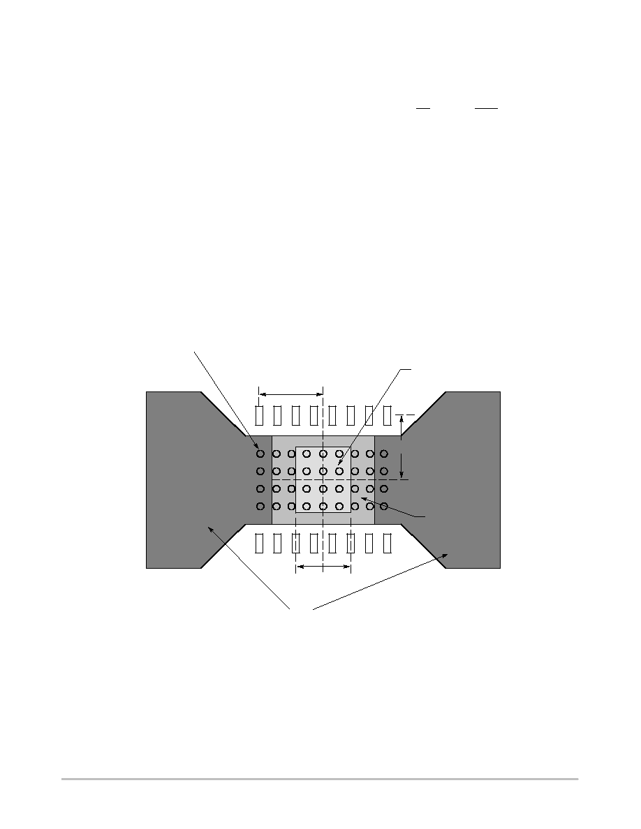
Package
The NCP3163 is contained in a heatsinkable 16-lead
plastic package in which the die is mounted on a special heat
tab copper alloy pad. This pad is designed to be soldered
directly to a GND connection on the printed circuit board to
improve thermal conduction. Since this pad directly
contacts the substrate of the die, it is important that this pad
be always soldered to GND, even if surface mount heat
sinking is not being used. Figure 21 shows recommended
layout techniques for this package.
Figure 21. Layout Guidelines to Obtain Maximum
Package Power Dissipation
Flare Metal for Maximum Heat Sinking
0.145
0.175
Exposed Pad
0.188
Vias to 2nd Layer Metal
for Maximum Heat Sinking
Minimum
Recommended
Exposed Copper
APPLICATIONS
Figures 23 through 30 show the simplicity and flexibility
of the NCP3163. Three main converter topologies are
demonstrated with actual test data shown below each of the
circuit diagrams. Figure 22 gives the relevant design
equations for the key parameters. Additionally, a complete
application design aid for the NCP3163 can be found at
www.onsemi.com.

NCP3163
http://onsemi.com
11
Calculation
Step-Down
Step-Up
Voltage-Inverting
ton
toff
(See Notes 1,2,3)
Vout
)
V
F
V
in
*
Vsat
*
Vout
Vout
)
V
F
≠ V
in
V
in
≠ Vsat
|Vout|
)
V
F
V
in
*
Vsat
ton
ton
t
off
ton
t
off
)
1
ton
t
off
ton
t
off
)
1
ton
t
off
ton
t
off
)
1
CT
32.143 ∑ 10
*
6
f
*
20
@
10
*
12
32.143 ∑ 10
*
6
f
*
20
@
10
*
12
32.143 ∑ 10
*
6
f
*
20
@
10
*
12
IL(avg)
Iout
Iout
ton
t
off
)
1
Iout
ton
t
off
)
1
Ipk (Switch)
IL(avg)
)
D
I
L
2
IL(avg)
)
D
I
L
2
IL(avg)
)
D
I
L
2
RSC
0.25
Ipk (Switch)
0.25
Ipk (Switch)
0.25
Ipk (Switch)
L
V
in
*
Vsat
*
Vout
D
I
L
ton
V
in
*
Vsat
D
I
L
ton
V
in
*
Vsat
D
I
L
ton
V
ripple(pp)
D
IL
1
8
CO
2
)
(ESR)2
[
ton Iout
C
O
[
ton Iout
C
O
Vout
V
ref
R
2
R
1
)
1
V
ref
R
2
R
1
)
1
V
ref
R
2
R
1
)
1
V
in
-
V
out
-
I
out
-
D
I
L
-
p
-
V
ripple(pp)
-
Nominal operating input voltage.
Desired output voltage.
Desired output current.
Desired peak-to-peak inductor ripple current. For maximum output current it is suggested that
D
I
L
be chosen to be less
than 10% of the average inductor current I
L(avg)
. This will help prevent I
pk (Switch)
from reaching the current limit
threshold set by R
SC
. If the design goal is to use a minimum inductance value, let
D
I
L
= 2(I
L(avg)
). This will
proportionally reduce converter output current capability.
Maximum output switch frequency.
Desired peak-to-peak output ripple voltage. For best performance the ripple voltage should be kept to a low value
since it will directly affect line and load regulation. Capacitor C
O
should be a low equivalent series resistance (ESR)
electrolytic designed for switching regulator applications.
The following Converter Characteristics must be chosen:
NOTES: 1. V
sat
- Saturation voltage of the output switch, refer to Figures 10 and 11.
NOTES:
2. V
F
- Output rectifier forward voltage drop. Typical value for 1N5822 Schottky barrier rectifier is 0.5 V.
NOTES:
3. The calculated t
on
/t
off
must not exceed the minimum guaranteed oscillator charge to discharge ratio of 8, at the minimum
NOTES: 3.
operating input voltage.
Figure 22. Design Equations

NCP3163
http://onsemi.com
12
R
B
L
D
LVI
1
+
+
-
Current
Limit
8
7
6
5
4
3
2
(Bottom View)
+
+
-
16
9
10
11
12
13
14
15
0.25 V
R
SC
V
in
C
T
1.125 V
15 k
1.25 V
45 k
Feedback
Comparator
Q
1
Q
2
60
C
in
C
O
C
B
V
out
-
+
Thermal
Oscillator
R
S
Q
Latch
2.0 mA
7.0 V
Figure 23. Typical Buck Application Schematic
V
CC
V
CC
V
CC
R
1
R
2
R
T
Value of Components
Name
Value
L
47
m
H
D
2 A, 40 V Schottky Rectifier
C
in
47
m
F, 35 V
C
out
100
m
F, 10 V
C
t
270 pF
±
10%
R
t
15 k
W
Name
Value
R
1
15 k
W
R
2
24.9 k
W
R
sc
80 m
W
, 1 W
C
b
4.7 nF
R
b
200
W
Test Results for V
out
= 3.3 V
Test
Condition
Results
Line Regulation
V
in
= 8.0 V to 24 V, I
out
= 2.5 A
13 mV
Load Regulation
V
in
= 12 V, I
out
= 0 to 2.5 A
25 mV
Output Ripple
V
in
= 12 V, I
out
= 0 to 2.5 A
100 mVpp
Efficiency
V
in
= 12 V, I
out
= 2.5 A
70.3%
Short Circuit Current
V
in
= 12 V, R
L
= 0.1
W
3.1 A
Test Results for V
out
= 5.05 V
Test
Condition
Results
Line Regulation
V
in
= 10.2 V to 24 V, I
out
= 2.5 A
54 mV
Load Regulation
V
in
= 12 V, I
out
= 0 to 2.5 A
28 mV
Output Ripple
V
in
= 12 V, I
out
= 0 to 2.5 A
150 mVpp
Efficiency
V
in
= 12 V, I
out
= 2.5 A
75.5%
Short Circuit Current
V
in
= 12 V, R
L
= 0.1
W
3.1 A
NCP3163
http://onsemi.com
13
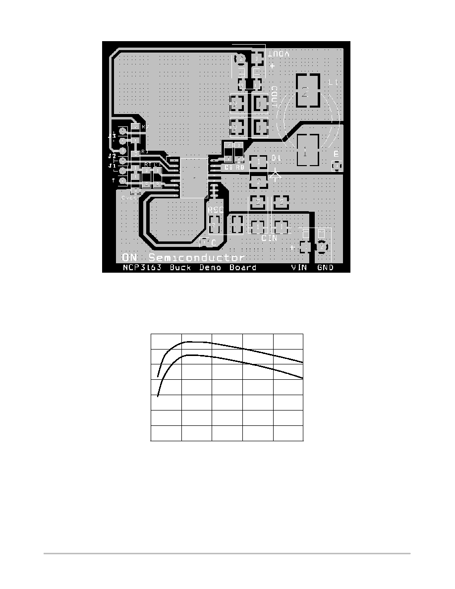
Figure 24. Buck Layout
APPLICATION SPECIFIC CHARACTERISTICS
Figure 25. Efficiency vs. Output Current for the
Buck Demo Board at V
in
= 12 V, T
A
= 25
5
C
I
out
(A)
EFFICIENCY
(%)
2.5
2.0
1.5
1.0
0.5
0
50
55
60
65
70
75
80
85
3.3 V Eff
5.0 V Eff

NCP3163
http://onsemi.com
14
LVI
1
+
+
-
Current
Limit
8
7
6
5
4
3
2
(Bottom View)
+
+
-
16
9
10
11
12
13
14
15
0.25 V
R
SC
V
in
C
T
1.125 V
15 k
1.25 V
45 k
Feedback
Comparator
Q
1
Q
2
60
C
in
C
O
V
out
+
D
R
1
R
2
-
+
Thermal
Oscillator
R
S
Q
Latch
2.0 mA
7.0 V
+
L
Figure 26. Typical Boost Application Schematic
V
CC
V
CC
V
CC
R
T
Value of Components for V
out
= 24 V
Name
Value
L
33
m
H
D
2 A, 40 V Schottky Rectifier
C
in
330
m
F, 35 V
C
t
270 pF
±
10%
R
t
15 k
W
Name
Value
R
1
42.2 k
W
R
2
2.32 k
W
C
out
330
m
F, 25 V
R
sc
80 m
W
, 1 W
Test Results for V
out
= 24 V
Test
Condition
Results
Line Regulation
V
in
= 10 V to 20 V, I
out
= 700 mA
90 mV
Load Regulation
V
in
= 12 V, I
out
= 0 to 700 mA
80 mV
Output Ripple
V
in
= 12 V, I
out
= 0 to 700 mA
300 mVpp
Efficiency
V
in
= 12 V, I
out
= 700 mA
83%
Short Circuit Current
V
in
= 12 V, R
L
= 0.1
W
3.1 A
NCP3163
http://onsemi.com
15
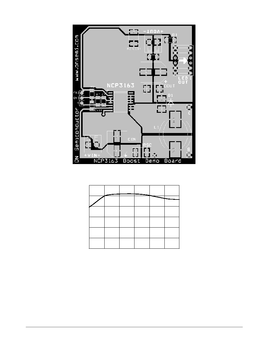
Figure 27. Boost Demo Board Layout
Figure 28. Efficiency vs. Output Current for the
Boost Demo Board at V
in
= 12 V, T
A
= 25
5
C
I
out
(A)
EFFICIENCY
(%)
0.7
0.5
0.4
0.3
0.2
0.1
74
76
78
80
82
84
86
0.6

NCP3163
http://onsemi.com
16
L
LVI
1
+
+
-
Current
Limit
8
7
6
5
4
3
2
(Bottom View)
+
+
-
16
9
10
11
12
13
14
15
0.25 V
R
SC
V
in
C
T
1.125 V
15 k
1.25 V
45 k
Feedback
Comparator
Q
1
Q
2
60
C
in
C
O
V
out
+
D
R
1
R
2
R
B
-
+
Thermal
Oscillator
R
S
Q
Latch
2.0 mA
7.0 V
+
C
B
Figure 29. Typical Voltage Inverting Application Schematic
R
T
V
CC
V
CC
V
CC
Value of Components for V
out
= -15 V
Name
Value
L
47
m
H
D
2 A, 40 V Schottky Rectifier
C
in
270
m
F, 16 V
C
out
2 X 270
m
F, 16 V
C
t
150 pF
±
10%
Name
Value
R
1
1.07 k
W
R
2
11.8 k
W
R
sc
80 m
W
, 1 W
C
b
4.7 nF
R
b
200 m
W
Test Results for V
out
= -15 V
Test
Condition
Results
Line Regulation
V
in
= 7.0 V to 16 V, I
out
= 500 mA
35 mV
Load Regulation
V
in
= 12 V, I
out
= 0 to 500 mA
20 mV
Output Ripple
V
in
= 12 V, I
out
= 0 to 500 mA
100 mVpp
Efficiency
V
in
= 12 V, I
out
= 500 mA
68%
Short Circuit Current
V
in
= 12 V, R
L
= 0.1
W
3.1 A

NCP3163
http://onsemi.com
17
Figure 30. Voltage Inverting Demo Board Layout
Figure 31. Efficiency vs. Output Current for the
Voltage Inverting Demo Board at V
in
= 12 V, T
A
= 25
5
C
I
out
(A)
EFFICIENCY
(%)
0.35
0.3
0.25
0.2
0.15
0.1
50
54
58
62
66
70
0.5
0.45
0.4
NCP3163
http://onsemi.com
18
ORDERING INFORMATION
Device
Package
Shipping
NCP3163PWG
SOIC-16 W Exposed Pad
(Pb-Free)
47 Units / Rail
NCP3163PWR2G
SOIC-16 W Exposed Pad
(Pb-Free)
1000 / Tape & Reel
NCP3163BPWG
SOIC-16 W Exposed Pad
(Pb-Free)
47 Units / Rail
NCP3163BPWR2G
SOIC-16 W Exposed Pad
(Pb-Free)
1000 / Tape & Reel
NCP3163MNR2G
DFN18
(Pb-Free)
2500 / Tape & Reel
NCP3163BMNR2G
DFN18
(Pb-Free)
2500 / Tape & Reel
For information on tape and reel specifications, including part orientation and tape sizes, please refer to our Tape and Reel Packaging
Specifications Brochure, BRD8011/D.
NCP3163
http://onsemi.com
19
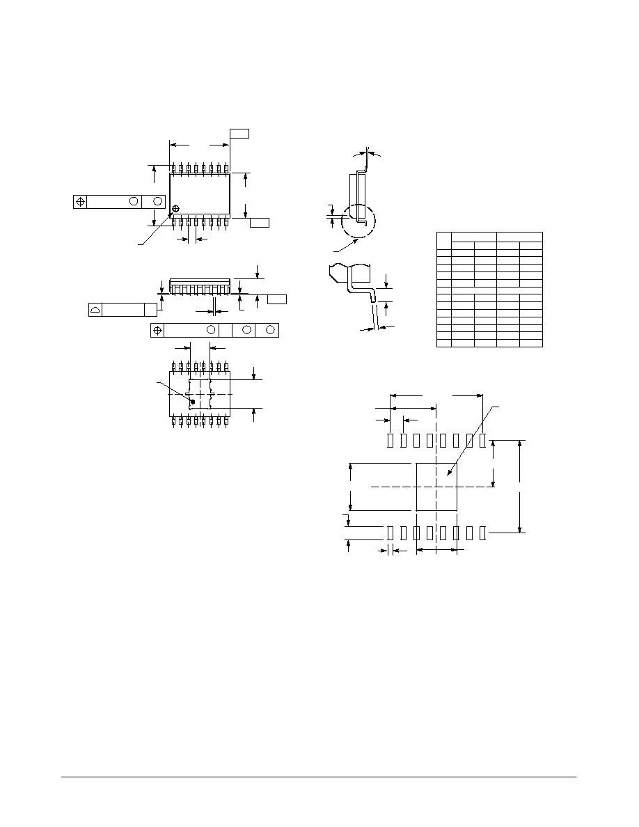
PACKAGE DIMENSIONS
SOIC 16 LEAD WIDE BODY, EXPOSED PAD
PW SUFFIX
CASE 751AG-01
ISSUE O
G
-W-
-U-
P
M
0.25 (0.010)
W
-T-
SEATING
PLANE
K
D
16 PL
C
M
0.25 (0.010)
T
U
W
S
S
M
F
DETAIL E
DETAIL E
R x 45
_
NOTES:
1. DIMENSIONING AND TOLERANCING PER ANSI
Y14.5M, 1982.
2. CONTROLLING DIMENSION: MILLIMETER.
3. DIMENSION A AND B DO NOT INCLUDE MOLD
PROTRUSION.
4. MAXIMUM MOLD PROTRUSION 0.15 (0.006) PER
SIDE.
5. DIMENSION D DOES NOT INCLUDE DAMBAR
PROTRUSION. ALLOWABLE PROTRUSION SHALL BE
0.13 (0.005) TOTAL IN EXCESS OF THE D DIMENSION
AT MAXIMUM MATERIAL CONDITION.
6. 751R-01 OBSOLETE, NEW STANDARD 751R-02.
J
M
14 PL
PIN 1 I.D.
8
1
16
9
TOP SIDE
0.10 (0.004) T
16
EXPOSED PAD
1
8
BACK SIDE
L
H
DIM
A
MIN
MAX
MIN
MAX
INCHES
10.15
10.45
0.400
0.411
MILLIMETERS
B
7.40
7.60
0.292
0.299
C
2.35
2.65
0.093
0.104
D
0.35
0.49
0.014
0.019
F
0.50
0.90
0.020
0.035
G
1.27 BSC
0.050 BSC
H
3.31
3.51
0.130
0.138
J
0.25
0.32
0.010
0.012
K
0.00
0.10
0.000
0.004
L
4.58
4.78
0.180
0.188
M
0
7
0
7
P
10.05
10.55
0.395
0.415
R
0.25
0.75
0.010
0.029
_
_
_
_
A
B
9
*For additional information on our Pb-Free strategy and soldering
details, please download the ON Semiconductor Soldering and
Mounting Techniques Reference Manual, SOLDERRM/D.
SOLDERING FOOTPRINT*
0.350
0.175
0.050
0.376
0.188
0.200
0.074
DIMENSIONS: MILLIMETERS
0.024
0.145
Exposed
Pad
CL
CL

NCP3163
http://onsemi.com
20
PACKAGE DIMENSIONS
18-LEAD DFN, 5 x 6 mm
MN SUFFIX
CASE 505-01
ISSUE B
C
0.15
E2
D2
L
b
18X
A
D
NOTES:
1. DIMENSIONS AND TOLERANCING PER
ASME Y14.5M, 1994.
2. DIMENSIONS IN MILLIMETERS.
3. DIMENSION b APPLIES TO PLATED
TERMINAL AND IS MEASURED BETWEEN
0.25 AND 0.30 MM FROM TERMINAL
4. COPLANARITY APPLIES TO THE EXPOSED
PAD AS WELL AS THE TERMINALS.
E
C
e
A
B
DIM
MIN
MAX
MILLIMETERS
A
0.80
1.00
A1
0.00
0.05
A3
0.20 REF
b
0.18
0.30
D
6.00 BSC
D2
3.98
4.28
E
5.00 BSC
E2
2.98
3.28
e
0.50 BSC
K
0.20
---
L
0.45
0.65
C
0.15
PIN 1 LOCATION
A1
(A3)
SEATING
PLANE
C
0.08
C
0.10
18X
K
18X
A
0.10
B
C
0.05 C
NOTE 3
1
9
10
18
2X
2X
18X
SIDE VIEW
TOP VIEW
BOTTOM VIEW
ON Semiconductor and are registered trademarks of Semiconductor Components Industries, LLC (SCILLC). SCILLC reserves the right to make changes without further notice
to any products herein. SCILLC makes no warranty, representation or guarantee regarding the suitability of its products for any particular purpose, nor does SCILLC assume any liability
arising out of the application or use of any product or circuit, and specifically disclaims any and all liability, including without limitation special, consequential or incidental damages.
"Typical" parameters which may be provided in SCILLC data sheets and/or specifications can and do vary in different applications and actual performance may vary over time. All
operating parameters, including "Typicals" must be validated for each customer application by customer's technical experts. SCILLC does not convey any license under its patent rights
nor the rights of others. SCILLC products are not designed, intended, or authorized for use as components in systems intended for surgical implant into the body, or other applications
intended to support or sustain life, or for any other application in which the failure of the SCILLC product could create a situation where personal injury or death may occur. Should
Buyer purchase or use SCILLC products for any such unintended or unauthorized application, Buyer shall indemnify and hold SCILLC and its officers, employees, subsidiaries, affiliates,
and distributors harmless against all claims, costs, damages, and expenses, and reasonable attorney fees arising out of, directly or indirectly, any claim of personal injury or death
associated with such unintended or unauthorized use, even if such claim alleges that SCILLC was negligent regarding the design or manufacture of the part. SCILLC is an Equal
Opportunity/Affirmative Action Employer. This literature is subject to all applicable copyright laws and is not for resale in any manner.
PUBLICATION ORDERING INFORMATION
N. American Technical Support: 800-282-9855 Toll Free
USA/Canada
Europe, Middle East and Africa Technical Support:
Phone: 421 33 790 2910
Japan Customer Focus Center
Phone: 81-3-5773-3850
NCP3163/D
LITERATURE FULFILLMENT:
Literature Distribution Center for ON Semiconductor
P.O. Box 5163, Denver, Colorado 80217 USA
Phone: 303-675-2175 or 800-344-3860 Toll Free USA/Canada
Fax: 303-675-2176 or 800-344-3867 Toll Free USA/Canada
Email: orderlit@onsemi.com
ON Semiconductor Website: www.onsemi.com
Order Literature: http://www.onsemi.com/orderlit
For additional information, please contact your local
Sales Representative