NCP3335A
©
Semiconductor Components Industries, LLC, 2005
December, 2005 - Rev. 2
1
Publication Order Number:
NCP3335A/D
NCP3335A
Ultra High Accuracy,
Low Iq, 500 mA
Low Dropout Regulator
The NCP3335A is a high performance, low dropout regulator. With
accuracy of
±0.9% over line and load and ultra-low quiescent current
and noise it encompasses all of the necessary features required by
today's consumer electronics. This unique device is guaranteed to be
stable without a minimum load current requirement and stable with
any type of capacitor as small as 1.0
mF. The NCP3335A also comes
equipped with sense and noise reduction pins to increase the overall
utility of the device. The NCP3335A offers reverse bias protection.
Features
·
High Accuracy Over Line and Load (
+0.9% at 255C)
·
Ultra-Low Dropout Voltage at Full Load (260 mV typ.)
·
No Minimum Output Current Required for Stability
·
Low Noise (35
mVrms w/10 nF C
nr
and 56
mVrms w/out C
nr
)
·
Low Shutdown Current (0.07
mA)
·
Reverse Bias Protected
·
2.6 V to 12 V Supply Range
·
Thermal Shutdown Protection
·
Current Limitation
·
Requires Only 1.0
mF Output Capacitance for Stability
·
Stable with Any Type of Capacitor (including MLCC)
·
Available in 2.5 V, 2.85 V, 3.3 V, 5.0 V and Adjustable Output
Voltages
·
These are Pb-Free Devices
Applications
·
PCMCIA Card
·
Cellular Phones
·
Camcoders and Cameras
·
Networking Systems, DSL/Cable Modems
·
Cable Set-Top Box
·
MP3/CD Players
·
DSP Supply
·
Displays and Monitors
Micro8
t
DM SUFFIX
CASE 846A
See detailed ordering and shipping information in the package
dimensions section on page 12 of this data sheet.
ORDERING INFORMATION
MARKING DIAGRAM
http://onsemi.com
Micro8
xxx = LIQ for 2.5 V
= LIR for 2.85 V
= LIS for 3.3 V
= LIT for 5.0 V
= LIO for Adj.
A
= Assembly Location
L
= Wafer Lot
Y
= Year
W
= Work Week
G
= Pb-Free Package
(Note: Microdot may be in either location)
xxx
AYW
G
G
1
8
Fixed Version
Pin 1, 2.
V
out
3. Sense
4. GND
5. NR
6. SD
7, 8. V
in
Adj Version
Pin 1, 2. V
out
3. Adj
4. GND
5. NR
6. SD
7, 8. V
in
DFN10
MN SUFFIX
CASE 485C
3335A
xxx
ALYW
G
G
1
Fixed Version
Pin 1, 2.
V
out
3. Sense
4. GND
5, 6. NC
7. NR
8. SD
9, 10. V
in
Adj Version
Pin 1, 2. V
out
3. Adj
4. GND
5, 6. NC
7. NR
8. SD
9, 10. V
in
DFN10
xxx = 25 for 2.5 V
= 285 for 2.85 V
= 33 for 3.3 V
= 50 for 5.0 V
= ADJ for Adj.
NCP3335A
http://onsemi.com
2
Figure 1. Typical Fixed Version Application Schematic (Micro8 Package)
V
in
V
out
ON
OFF
C
in
1.0
m
F
C
out
1.0
m
F
OUT
SENSE
OUT
IN
IN
NR
3
2
1
7
8
(Optional)
6
4
+
+
5
GND
SD
C
nr
Figure 2. Typical Adjustable Version Application Schematic (Micro8 Package)
V
in
V
out
ON
OFF
C
in
1.0
m
F
C
out
1.0
m
F
OUT
ADJ
IN
IN
NR
3
2
1
7
8
6
4
+
+
5
GND
SD
C
nr
10 nF
(Optional)
OUT
R2
R1
C
ADJ
68 pF
NCP3335A
http://onsemi.com
3
PIN FUNCTION DESCRIPTION
Fixed Version
Micro8
Pin No.
DFN10
Pin No.
Pin Name
Description
1, 2
1, 2
V
out
Regulated output voltage. Bypass to ground with C
out
w
1.0
m
F.
3
3
SENSE
For output voltage sensing, connect to Pins 1 and 2.
4
4
GND
Power Supply Ground
5
7
NR
Noise Reduction Pin. This is an optional pin used to further reduce noise.
6
8
SD
Shutdown pin. When not in use, this pin should be connected to the input pin.
7, 8
9, 10
V
in
Power Supply Input Voltage
-
5, 6
NC
Not Connected
Adjustable Version
1, 2
1, 2
V
out
Regulated output voltage. Bypass to ground with C
out
w
1.0
m
F.
3
3
Adj
Adjustable pin; reference voltage = 1.25 V.
4
4
GND
Power Supply Ground
5
7
NR
Noise Reduction Pin. This is an optional pin used to further reduce noise.
6
8
SD
Shutdown pin. When not in use, this pin should be connected to the input pin.
7, 8
9, 10
V
in
Power Supply Input Voltage
-
5, 6
NC
Not Connected
MAXIMUM RATINGS
Rating
Symbol
Value
Unit
Input Voltage
V
in
-0.3 to +16
V
Output Voltage
V
out
-0.3 to V
in
+0.3 or 10 V*
V
Shutdown Pin Voltage
V
sh
-0.3 to +16
V
Thermal Characteristics
Thermal Resistance, Junction-to-Air
R
q
JA
238
°
C/W
Operating Junction Temperature Range, Micro8
T
J
-40 to +150
°
C
Storage Temperature Range
T
stg
-50 to+150
°
C
Maximum ratings are those values beyond which device damage can occur. Maximum ratings applied to the device are individual stress limit
values (not normal operating conditions) and are not valid simultaneously. If these limits are exceeded, device functional operation is not implied,
damage may occur and reliability may be affected.
NOTE:
This device series contains ESD protection and exceeds the following tests:
Human Body Model (HBM) JESD 22-A114-B
Machine Model (MM) JESD 22-A115-A
*Which ever is less. Reverse bias protection feature valid only if V
out
- V
in
7 V.
NCP3335A
http://onsemi.com
4
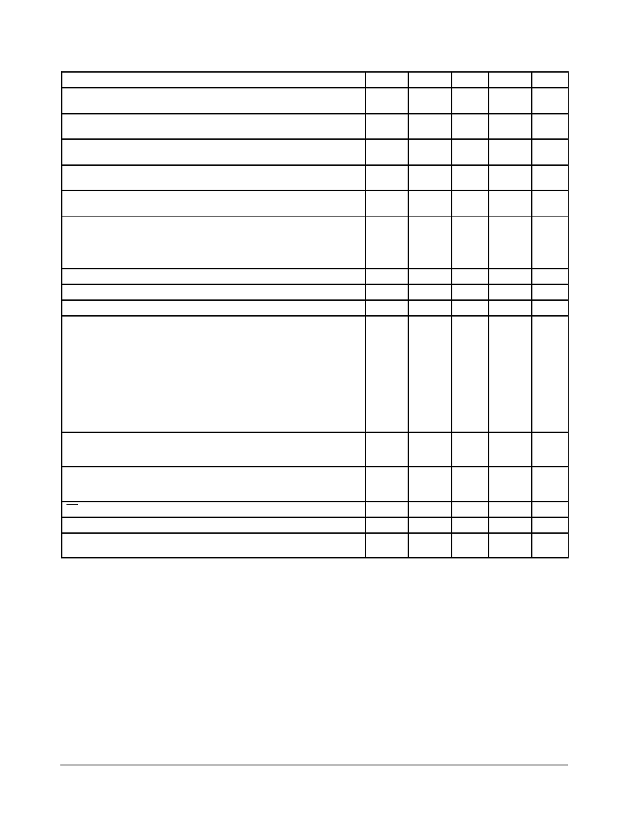
ELECTRICAL CHARACTERISTICS - 2.5 V
(V
out
= 2.5 V typical, V
in
= 2.9 V, T
A
= -40
°
C to +85
°
C, unless otherwise noted)
Characteristic
Symbol
Min
Typ
Max
Unit
Output Voltage (Accuracy)
V
in
= 2.9 V to 6.5 V, I
load
= 0.1 mA to 500 mA, T
J
= 25
°
C
V
out
-0.9%
2.477
2.5
+0.9%
2.523
V
Output Voltage (Accuracy)
V
in
= 2.9 V to 6.5 V, I
load
= 0.1 mA to 500 mA, T
J
= 0
°
C to +85
°
C
V
out
-1.4%
2.465
2.5
+1.4%
2.535
V
Output Voltage (Accuracy), (Note 1)
V
in
= 2.9 V to 6.5 V, I
load
= 0.1 mA to 500 mA, T
J
= -40
°
C to +150
°
C
V
out
-1.5%
2.462
2.5
+1.5%
2.538
V
Line Regulation
V
in
= 2.9 V to 12 V, I
load
= 0.1 mA
Line
Reg
0.04
mV/V
Load Regulation
V
in
= 2.9 V, I
load
= 0.1 mA to 500 mA
Load
Reg
0.04
mV/mA
Dropout Voltage (See App Note)
I
load
= 500 mA (Note 2)
I
load
= 300 mA (Note 2)
I
load
= 50 mA
I
load
= 0.1mA
V
DO
340
230
110
10
mV
Peak Output Current (See Figure 7)
I
pk
500
700
800
mA
Short Output Current (See Figure 7)
I
sc
900
mA
Thermal Shutdown
T
J
160
°
C
Ground Current
In Regulation
I
load
= 500 mA (Note 2)
I
load
= 300 mA (Note 2)
I
load
= 50 mA
I
load
= 0.1 mA
In Dropout
V
in
= 2.4 V, I
load
= 0.1 mA
In Shutdown
S
D
= 0 V
I
GND
I
GNDsh
9.0
4.6
0.8
-
0.07
14
7.5
2.5
190
500
1.0
mA
m
A
m
A
m
A
Output Noise
C
nr
= 0 nF, I
load
= 500 mA, f = 10 Hz to 100 kHz, C
out
= 10
m
F
C
nr
= 10 nF, I
load
= 500 mA, f = 10 Hz to 100 kHz, C
out
= 10
m
F
V
noise
56
35
m
Vrms
m
Vrms
Shutdown
Threshold Voltage ON
Threshold Voltage OFF
2.0
0.4
V
V
SD Input Current, V
SD
= 0 V to 0.4 V or V
SD
= 2.0 V to V
in
I
SD
0.07
1.0
m
A
Output Current In Shutdown Mode, V
out
= 0 V
I
OSD
0.07
1.0
m
A
Reverse Bias Protection, Current Flowing from the Output Pin to GND
(V
in
= 0 V, V
out_forced
= 2.5 V)
I
OUTR
10
m
A
1. For output current capability for T
J
< 0
°
C, please refer to Figure 9.
2. T
A
must be greater than 0
°
C.

NCP3335A
http://onsemi.com
5
ELECTRICAL CHARACTERISTICS - 2.85 V
(V
out
= 2.85 V typical, V
in
= 3.25 V, T
A
= -40
°
C to +85
°
C, unless otherwise noted)
Characteristic
Symbol
Min
Typ
Max
Unit
Output Voltage (Accuracy)
V
in
= 3.25 V to 6.85 V, I
load
= 0.1 mA to 500 mA, T
J
= 25
°
C
V
out
-0.9%
2.824
2.85
+0.9%
2.876
V
Output Voltage (Accuracy)
V
in
= 3.25 V to 6.85 V, I
load
= 0.1 mA to 500 mA, T
J
= 0
°
C to +85
°
C
V
out
-1.4%
2.810
2.85
+1.4%
2.890
V
Output Voltage (Accuracy) (Note 3)
V
in
= 3.25 V to 6.85 V, I
load
= 0.1 mA to 500 mA, T
J
= -40
°
C to +150
°
C
V
out
-1.5%
2.807
2.85
+1.5%
2.893
V
Line Regulation
V
in
= 3.25 V to 12 V, I
load
= 0.1 mA
Line
Reg
0.04
mV/V
Load Regulation
V
in
= 3.25 V, I
load
= 0.1 mA to 500 mA
Load
Reg
0.04
mV/mA
Dropout Voltage (See App Note)
I
load
= 500 mA
I
load
= 300 mA
I
load
= 50 mA
I
load
= 0.1mA
V
DO
340
230
110
10
mV
Peak Output Current (See Figure 7)
I
pk
500
700
800
mA
Short Output Current (See Figure 7)
I
sc
900
mA
Thermal Shutdown
T
J
160
°
C
Ground Current
In Regulation
I
load
= 500 mA (Note 4)
I
load
= 300 mA
I
load
= 50 mA
I
load
= 0.1 mA
In Dropout
V
in
= 2.75 V, I
load
= 0.1 mA
In Shutdown
SD = 0 V
I
GND
I
GNDsh
9.0
4.6
0.8
-
-
0.07
14
7.5
2.5
190
500
1.0
mA
m
A
m
A
m
A
Output Noise
C
nr
= 0 nF, I
load
= 500 mA, f = 10 Hz to 100 kHz, C
out
= 10
m
F
C
nr
= 10 nF, I
load
= 500 mA, f = 10 Hz to 100 kHz, C
out
= 10
m
F
V
noise
61
40
m
Vrms
m
Vrms
Shutdown
Threshold Voltage ON
Threshold Voltage OFF
2.0
0.4
V
V
S
D
Input Current, V
SD
= 0 V to 0.4 V or V
SD
= 2.0 V to V
in
I
SD
0.07
1.0
m
A
Output Current In Shutdown Mode, V
out
= 0 V
I
OSD
0.07
1.0
m
A
Reverse Bias Protection, Current Flowing from the Output Pin to GND
(V
in
= 0 V, V
out_forced
= 2.85 V)
I
OUTR
10
m
A
3. For output current capability for T
J
< 0
°
C, please refer to Figure 8.
4. T
A
must be greater than 0
°
C.

NCP3335A
http://onsemi.com
6
ELECTRICAL CHARACTERISTICS 3.3 V
(V
out
= 3.3 V typical, V
in
= 3.7 V, T
A
= -40
°
C to +85
°
C, unless otherwise noted)
Characteristic
Symbol
Min
Typ
Max
Unit
Output Voltage (Accuracy)
V
in
= 3.7 V to 7.3 V, I
load
= 0.1 mA to 500 mA, T
J
= 25
°
C
V
out
-0.9%
3.270
3.3
+0.9%
3.330
V
Output Voltage (Accuracy)
V
in
= 3.7 V to 7.3 V, I
load
= 0.1 mA to 500 mA, T
J
= 0
°
C to +85
°
C
V
out
-1.4%
3.254
3.3
+1.4%
3.346
V
Output Voltage (Accuracy)
V
in
= 3.7 V to 7.3 V, I
load
= 0.1 mA to 500 mA, T
J
= -40
°
C to +150
°
C
V
out
-1.5%
3.250
3.3
+1.5%
3.350
V
Line Regulation
V
in
= 3.7 V to 12 V, I
load
= 0.1 mA
Line
Reg
0.04
mV/V
Load Regulation
V
in
= 3.7 V, I
load
= 0.1 mA to 500 mA
Load
Reg
0.04
mV/mA
Dropout Voltage (See App Note)
I
load
= 500 mA
I
load
= 300 mA
I
load
= 50 mA
I
load
= 0.1 mA
V
DO
340
230
110
10
mV
Peak Output Current (See Figure 7)
Ipk
500
700
800
mA
Short Output Current (See Figure 7)
I
sc
900
mA
Thermal Shutdown
T
J
160
°
C
Ground Current
In Regulation
I
load
= 500 mA (Note 5)
I
load
= 300 mA
I
load
= 50 mA
I
load
= 0.1 mA
In Dropout
V
in
= 3.2 V, I
load
= 0.1 mA
In Shutdown
S
D
= 0 V
I
GND
I
GNDsh
9.0
4.6
0.8
-
-
0.07
14
7.5
2.5
190
500
1.0
mA
m
A
m
A
m
A
Output Noise
C
nr
= 0 nF, I
load
= 500 mA, f = 10 Hz to 100 kHz, C
out
= 10
m
F
C
nr
= 10 nF, I
load
= 500 mA, f = 10 Hz to 100 kHz, C
out
= 10
m
F
V
noise
69
46
m
Vrms
m
Vrms
Shutdown
Threshold Voltage ON
Threshold Voltage OFF
2.0
0.4
V
V
S
D
Input Current, V
SD
= 0 V to 0.4 V or V
SD
= 2.0 V to V
in
I
SD
0.07
1.0
m
A
Output Current In Shutdown Mode, V
out
= 0 V
I
OSD
0.07
1.0
m
A
Reverse Bias Protection, Current Flowing from the Output Pin to GND
(V
in
= 0 V, V
out_forced
= 3.3 V)
I
OUTR
10
m
A
5. T
A
must be greater than 0
°
C.
NCP3335A
http://onsemi.com
7
ELECTRICAL CHARACTERISTICS 5.0 V
(V
out
= 5.0 V typical, V
in
= 5.4 V, T
A
= -40
°
C to +85
°
C, unless otherwise noted)
Characteristic
Symbol
Min
Typ
Max
Unit
Output Voltage (Accuracy)
V
in
= 5.4 V to 9.0 V, I
load
= 0.1 mA to 500 mA, T
J
= 25
°
C
V
out
-0.9%
4.955
5.0
+0.9%
5.045
V
Output Voltage (Accuracy)
V
in
= 5.4 V to 9.0 V, I
load
= 0.1 mA to 500 mA, T
J
= 0
°
C to +85
°
C
V
out
-1.4%
4.930
5.0
+1.4%
5.070
V
Output Voltage (Accuracy)
V
in
= 5.4 V to 9.0 V, I
load
= 0.1 mA to 500 mA, T
J
= -40
°
C to +150
°
C
V
out
-1.5%
4.925
5.0
+1.5%
5.075
V
Line Regulation
V
in
= 5.4 V to 12 V, I
load
= 0.1 mA
Line
Reg
0.04
mV/V
Load Regulation
V
in
= 5.4 V, I
load
= 0.1 mA to 500 mA
Load
Reg
0.04
mV/mA
Dropout Voltage (See App Note)
I
load
= 500 mA
I
load
= 300 mA
I
load
= 50 mA
I
load
= 0.1 mA
V
DO
340
230
110
10
mV
Peak Output Current (See Figure 7)
Ipk
500
700
830
mA
Short Output Current (See Figure 7)
I
sc
930
mA
Thermal Shutdown
T
J
160
°
C
Ground Current
In Regulation
I
load
= 500 mA (Note 6)
I
load
= 300 mA (Note 6)
I
load
= 50 mA
I
load
= 0.1 mA
In Dropout
V
in
= V
out
-0.1 V, I
load
= 0.1 mA
In Shutdown
S
D
= 0 V
I
GND
I
GNDsh
9.0
4.6
0.8
-
-
0.07
14
7.5
2.5
190
500
1.0
mA
m
A
m
A
m
A
Output Noise
C
nr
= 0 nF, I
load
= 500 mA, f = 10 Hz to 100 kHz, C
out
= 10
m
F
C
nr
= 10 nF, I
load
= 500 mA, f = 10 Hz to 100 kHz, C
out
= 10
m
F
V
noise
93
58
m
Vrms
m
Vrms
Shutdown
Threshold Voltage ON
Threshold Voltage OFF
2.0
0.4
V
V
S
D
Input Current, V
SD
= 0 V to 0.4 V or V
SD
= 2.0 V to V
in
I
SD
0.07
1.0
m
A
Output Current In Shutdown Mode, V
out
= 0 V
I
OSD
0.07
1.0
m
A
Reverse Bias Protection, Current Flowing from the Output Pin to GND
(V
in
= 0 V, V
out_forced
= 5.0 V)
I
OUTR
10
m
A
6. T
A
must be greater than 0
°
C.
NCP3335A
http://onsemi.com
8
ELECTRICAL CHARACTERISTICS Adjustable
(V
out
= 1.25 V typical, V
in
= 2.9 V, T
A
= -40
°
C to +85
°
C, unless otherwise noted)
Characteristic
Symbol
Min
Typ
Max
Unit
Reference Voltage (Accuracy)
V
in
= 2.9 V to V
out
+ 4.0 V, I
load
= 0.1 mA to 500 mA, T
J
= 25
°
C
V
ref
-0.9%
1.239
1.25
+0.9%
1.261
V
Reference Voltage (Accuracy)
V
in
= 2.9 V to V
out
+ 4.0 V, I
load
= 0.1 mA to 500 mA, T
J
= 0
°
C to +85
°
C
V
ref
-1.4%
1.233
1.25
+1.4%
1.268
V
Reference Voltage (Accuracy) (Note 7)
V
in
= 2.9 V to V
out
+ 4.0 V, I
load
= 0.1 mA to 500 mA, T
J
= -40
°
C to +150
°
C
V
ref
-1.5%
1.231
1.25
+1.5%
1.269
V
Line Regulation
V
in
= 2.9 V to 12 V, I
load
= 0.1 mA
Line
Reg
0.04
mV/V
Load Regulation
V
in
= 2.9 V, I
load
= 0.1 mA to 500 mA
Load
Reg
0.04
mV/mA
Dropout Voltage (See App Note), V
out
= 2.5 V to 10 V
I
load
= 500 mA (Note 8)
I
load
= 300 mA
I
load
= 50 mA
I
load
= 0.1 mA
V
DO
340
230
110
10
mV
Peak Output Current (Note 8) (See Figure 7)
Ipk
500
700
860
mA
Short Output Current (See Figure 7)
V
out
3.3 V
V
out
> 3.3 V
I
sc
900
990
mA
Thermal Shutdown
T
J
160
°
C
Ground Current
In Regulation
I
load
= 500 mA (Note 8)
I
load
= 300 mA (Note 8)
I
load
= 50 mA
I
load
= 0.1 mA
In Dropout
V
in
= V
out
-0.1 V, I
load
= 0.1 mA
In Shutdown
S
D
= 0 V
I
GND
I
GNDsh
9.0
4.6
0.8
-
-
0.07
14
7.5
2.5
190
500
1.0
mA
m
A
m
A
m
A
Output Noise
C
nr
= 0 nF, I
load
= 500 mA, f = 10 Hz to 100 kHz, C
out
= 10
m
F
C
nr
= 10 nF, I
load
= 500 mA, f = 10 Hz to 100 kHz, C
out
= 10
m
F
V
noise
38
26
m
Vrms
m
Vrms
Shutdown
Threshold Voltage ON
Threshold Voltage OFF
2.0
0.4
V
V
S
D
Input Current, V
SD
= 0 V to 0.4 V or V
SD
= 2.0 V to V
in
V
in
5.4 V
V
in
> 5.4 V
I
SD
0.07
1.0
5.0
m
A
Output Current In Shutdown Mode, V
out
= 0 V
I
OSD
0.07
1.0
m
A
Reverse Bias Protection, Current Flowing from the Output Pin to GND
(V
in
= 0 V, V
out_forced
= V
out
(nom)
7 V) (Note 9)
I
OUTR
1.0
m
A
7. For output current capability for T
J
< 0
°
C, please refer to Figure 9.
8. T
A
must be greater than 0
°
C.
9. Reverse bias protection feature valid only if V
out
- V
in
7 V.
NCP3335A
http://onsemi.com
9
0
50
100
150
200
250
300
350
400
0
20
40
60
80
100
120
140
T
J
(
°
C)
V
DO
(mV)
Figure 3. Dropout Voltage vs. Temperature
50 mA
500 mA
300 mA
0
2
4
6
8
10
12
0
20
40
60
80
100
120
140
T
J
(
°
C)
I
GND
(mA)
Figure 4. Ground Current vs. Temperature
500 mA
300 mA
50 mA
2.450
2.460
2.470
2.480
2.490
2.500
2.510
2.520
2.530
2.540
2.550
-40
-20
0
20
40
60
80
100
120
140
T
J
(
°
C)
V
OUT
(V)
Figure 5. Output Voltage vs. Temperature
0
100
200
300
400
500
600
700
800
900
1000
0
20
40
60
80
100
120
140
I
sc
I
pk
T
J
(
°
C)
I
pk
(mA), I
sc
(mA)
Figure 6. Peak and Short Current
vs. Temperature
I
out
(mA)
(For specific values of I
pk
and I
sc
, please refer to Figure 6)
V
out
(V)
Figure 7. Output Voltage vs. Output Current
I
sc
I
pk
0.97 V
out
NCP3335A
http://onsemi.com
10
V
IN
(V)
I
OUT
(A)
Figure 8. Output Current Capability for the
2.85 V Version
V
IN
, (V)
I
OUT
, (A)
Figure 9. Output Current Capability for the
2.5 V Version
0
0.1
0.2
0.3
0.4
0.5
0.6
0.7
0.8
2.5
2.6
2.7
2.8
2.9
3.0
3.1
3.2
3.3
3.4
3.5
0
°
C
-40
°
C
-30
°
C
-20
°
C
-10
°
C
0
0.1
0.2
0.3
0.4
0.5
0.6
0.7
0.8
2.85
2.95
3.05
3.15
3.25
3.35
3.45
3.55
3.65
3.75
3.85
0
°
C
-20
°
C
-40
°
C
0
10
20
30
40
50
60
70
80
90
100
0.01
0.1
1.0
10
100
F, FREQUENCY (kHz)
RR, RIPPLE REJECTION (dB)
Figure 10. Ripple Rejection vs. Frequency
50 mA
500 mA
250 mA
V
out
= 2.5 V
C
out
= 10
m
F
T
J
= 25
°
C
0
50
100
150
200
250
300
350
400
450
500
0.01
0.1
1.0
10
100
F, FREQUENCY (kHz)
Figure 11. Output Noise Density
V
out
= 2.5 V
I
out
= 500 mA
T
J
= 25
°
C
C
out
= 10
m
F
C
nr
= 0 nF
C
out
= 1.0
m
F
C
nr
= 0 nF
C
out
= 1.0
m
F
C
nr
= 10 nF
C
out
= 10
m
F
C
nr
= 10 nF
NOISE DENSITY (nV/
Hz
)
5.10
5.05
5.00
4.95
4.90
4.85
135
110
85
60
35
10
-15
-40
150
OUTPUT VOL
T
AGE, V
OUT
(V)
TEMPERATURE (
°
C)
V
OUT
= 5 V
Figure 12. Output Voltage vs. Temperature

NCP3335A
http://onsemi.com
11
APPLICATIONS INFORMATION
Reverse Bias Protection
Reverse bias is a condition caused when the input voltage
goes to zero, but the output voltage is kept high either by a
large output capacitor or another source in the application
which feeds the output pin.
Normally in a bipolar LDO all the current will flow from
the output pin to input pin through the PN junction with
limited current capability and with the potential to destroy
the IC.
Due to an improved architecture, the NCP3335A can
withstand up to 7.0 V on the output pin with virtually no
current flowing from output pin to input pin, and only
negligible amount of current (tens of
mA) flowing from the
output pin to ground for infinite duration.
Input Capacitor
An input capacitor of at least 1.0
mF, any type, is
recommended to improve the transient response of the
regulator and/or if the regulator is located more than a few
inches from the power source. It will also reduce the circuit's
sensitivity to the input line impedance at high frequencies.
The capacitor should be mounted with the shortest possible
track length directly across the regular's input terminals.
Output Capacitor
The NCP3335A remains stable with any type of capacitor
as long as it fulfills its 1.0
mF requirement. There are no
constraints on the minimum ESR and it will remain stable up
to an ESR of 5.0
W. Larger capacitor values will improve the
noise rejection and load transient response.
Noise Reduction Pin
Output noise can be greatly reduced by connecting a 10 nF
capacitor (C
nr
) between the noise reduction pin and ground
(see Figure 1). In applications where very low noise is not
required, the noise reduction pin can be left unconnected.
For the adjustable version, in addition to the 10 nF C
nr
, a
68 pF capacitor connected in parallel with R1 (see Figure 2)
is recommended to further reduce output noise and improve
stability.
Adjustable Operation
The output voltage can be set by using a resistor divider
as shown in Figure 2 with a range of 1.25 to 10 V. The
appropriate resistor divider can be found by solving the
equation below. The recommended current through the
resistor divider is from 10
mA to 100 mA. This can be
accomplished by selecting resistors in the k
W range. As
result, the I
adj
*R2 becomes negligible in the equation and
can be ignored.
Vout
+
1.25 * 1
)
R1
R2
)
Iadj * R2
(eq. 1)
Example:
For V
out
= 2.9 V, can use R
1
= 36 k
W and R
2
= 27 k
W.
1.25 * 1
)
36 k
W
27 k
W +
2.91 V
(eq. 2)
Dropout Voltage
The voltage dropout is measured at 97% of the nominal
output voltage.
Thermal Considerations
Internal thermal limiting circuitry is provided to protect the
integrated circuit in the event that the maximum junction
temperature is exceeded. This feature provides protection
from a catastrophic device failure due to accidental
overheating. This protection feature is not intended to be used
as a substitute to heat sinking. The maximum power that can
be dissipated, can be calculated with the equation below:
PD
+
TJ(max)
*
TA
R
q
JA
(eq. 3)
For improved thermal performance, contact the factory
for the DFN package option. The DFN package includes an
exposed metal pad that is specifically designed to reduce the
junction to air thermal resistance, R
qJA
.
NCP3335A
http://onsemi.com
12
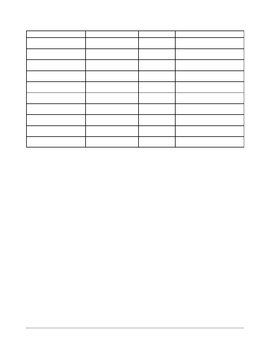
ORDERING INFORMATION
Device
Nominal Output Voltage
Package
Shipping
NCP3335ADM250R2G
2.5 V
Micro8
(Pb-Free)
4000 / Tape & Reel
NCP3335ADM285R2G
2.85 V
Micro8
(Pb-Free)
4000 / Tape & Reel
NCP3335ADM330R2G
3.3 V
Micro8
(Pb-Free)
4000 / Tape & Reel
NCP3335ADM500R2G
5.0 V
Micro8
(Pb-Free)
4000 / Tape & Reel
NCP3335ADMADJR2G
Adj.
Micro8
(Pb-Free)
4000 / Tape & Reel
NCP3335AMN250R2G
2.5 V
DFN10
(Pb-Free)
3000 / Tape & Reel
NCP3335AMN285R2G
2.85 V
DFN10
(Pb-Free)
3000 / Tape & Reel
NCP3335AMN330R2G
3.3 V
DFN10
(Pb-Free)
3000 / Tape & Reel
NCP3335AMN500R2G
5.0 V
DFN10
(Pb-Free)
3000 / Tape & Reel
NCP3335AMNADJR2G
Adj.
DFN10
(Pb-Free)
3000 / Tape & Reel
For information on tape and reel specifications, including part orientation and tape sizes, please refer to our Tape and Reel Packaging
Specifications Brochure, BRD8011/D.
*Please contact factory for other voltage options.
NCP3335A
http://onsemi.com
13
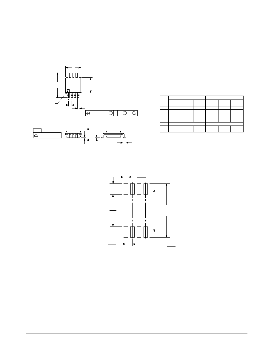
PACKAGE DIMENSIONS
Micro8
CASE 846A-02
ISSUE G
8X
8X
6X
mm
inches
SCALE 8:1
1.04
0.041
0.38
0.015
5.28
0.208
4.24
0.167
3.20
0.126
0.65
0.0256
*For additional information on our Pb-Free strategy and soldering
details, please download the ON Semiconductor Soldering and
Mounting Techniques Reference Manual, SOLDERRM/D.
SOLDERING FOOTPRINT*
S
B
M
0.08 (0.003)
A
S
T
NOTES:
1. DIMENSIONING AND TOLERANCING PER ANSI Y14.5M, 1982.
2. CONTROLLING DIMENSION: MILLIMETER.
3. DIMENSION A DOES NOT INCLUDE MOLD FLASH, PROTRUSIONS OR GATE
BURRS. MOLD FLASH, PROTRUSIONS OR GATE BURRS SHALL NOT EXCEED
0.15 (0.006) PER SIDE.
4. DIMENSION B DOES NOT INCLUDE INTERLEAD FLASH OR PROTRUSION.
INTERLEAD FLASH OR PROTRUSION SHALL NOT EXCEED 0.25 (0.010) PER SIDE.
5. 846A-01 OBSOLETE, NEW STANDARD 846A-02.
b
e
PIN 1 ID
8 PL
0.038 (0.0015)
-T-
SEATING
PLANE
A
A1
c
L
DIM
A
MIN
NOM
MAX
MIN
MILLIMETERS
--
--
1.10
--
INCHES
A1
0.05
0.08
0.15
0.002
b
0.25
0.33
0.40
0.010
c
0.13
0.18
0.23
0.005
D
2.90
3.00
3.10
0.114
E
2.90
3.00
3.10
0.114
e
0.65 BSC
L
0.40
0.55
0.70
0.016
--
0.043
0.003
0.006
0.013
0.016
0.007
0.009
0.118
0.122
0.118
0.122
0.026 BSC
0.021
0.028
NOM
MAX
4.75
4.90
5.05
0.187
0.193
0.199
H
E
H
E
D
D
E
NCP3335A
http://onsemi.com
14
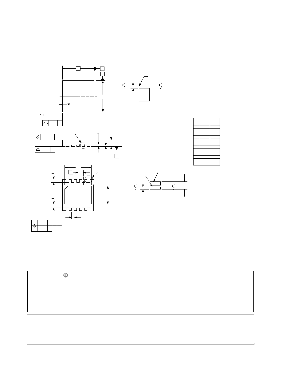
PACKAGE DIMENSIONS
DFN10
CASE 485C-01
ISSUE A
10X
SEATING
PLANE
L
D
E
0.15 C
A
A1
e
D2
E2
b
1
5
10
6
NOTES:
1. DIMENSIONING AND TOLERANCING PER
ASME Y14.5M, 1994.
2. CONTROLLING DIMENSION: MILLIMETERS.
3. DIMENSION b APPLIES TO PLATED
TERMINAL AND IS MEASURED BETWEEN
0.25 AND 0.30 MM FROM TERMINAL.
4. COPLANARITY APPLIES TO THE EXPOSED
PAD AS WELL AS THE TERMINALS.
5. TERMINAL b MAY HAVE MOLD COMPOUND
MATERIAL ALONG SIDE EDGE. MOLD
FLASHING MAY NOT EXCEED 30 MICRONS
ONTO BOTTOM SURFACE OF TERMINAL b.
6. DETAILS A AND B SHOW OPTIONAL VIEWS
FOR END OF TERMINAL LEAD AT EDGE OF
PACKAGE.
ÇÇÇÇ
ÇÇÇÇ
ÇÇÇÇ
B
A
0.15 C
TOP VIEW
SIDE VIEW
BOTTOM VIEW
PIN 1
REFERENCE
0.10 C
0.08 C
(A3)
C
10X
10X
0.10 C
0.05 C
A B
NOTE 3
K
10X
DIM
MIN
MAX
MILLIMETERS
A
0.80
1.00
A1
0.00
0.05
A3
0.20 REF
b
0.18
0.30
D
3.00 BSC
D2
2.45
2.55
E
3.00 BSC
E2
1.75
1.85
e
0.50 BSC
L
0.35
0.45
L1
0.00
0.03
DETAIL A
K
0.19 TYP
2X
2X
L1
DETAIL A
Bottom View
(Optional)
ÉÉ
ÉÉ
ÉÉ
A1
A3
DETAIL B
Side View
(Optional)
EDGE OF PACKAGE
MOLD CMPD
EXPOSED Cu
DETAIL B
ON Semiconductor and are registered trademarks of Semiconductor Components Industries, LLC (SCILLC). SCILLC reserves the right to make changes without further notice
to any products herein. SCILLC makes no warranty, representation or guarantee regarding the suitability of its products for any particular purpose, nor does SCILLC assume any liability
arising out of the application or use of any product or circuit, and specifically disclaims any and all liability, including without limitation special, consequential or incidental damages.
"Typical" parameters which may be provided in SCILLC data sheets and/or specifications can and do vary in different applications and actual performance may vary over time. All
operating parameters, including "Typicals" must be validated for each customer application by customer's technical experts. SCILLC does not convey any license under its patent rights
nor the rights of others. SCILLC products are not designed, intended, or authorized for use as components in systems intended for surgical implant into the body, or other applications
intended to support or sustain life, or for any other application in which the failure of the SCILLC product could create a situation where personal injury or death may occur. Should
Buyer purchase or use SCILLC products for any such unintended or unauthorized application, Buyer shall indemnify and hold SCILLC and its officers, employees, subsidiaries, affiliates,
and distributors harmless against all claims, costs, damages, and expenses, and reasonable attorney fees arising out of, directly or indirectly, any claim of personal injury or death
associated with such unintended or unauthorized use, even if such claim alleges that SCILLC was negligent regarding the design or manufacture of the part. SCILLC is an Equal
Opportunity/Affirmative Action Employer. This literature is subject to all applicable copyright laws and is not for resale in any manner.
PUBLICATION ORDERING INFORMATION
N. American Technical Support: 800-282-9855 Toll Free
USA/Canada
Japan: ON Semiconductor, Japan Customer Focus Center
2-9-1 Kamimeguro, Meguro-ku, Tokyo, Japan 153-0051
Phone: 81-3-5773-3850
NCP3335A/D
The products described herein NCP3335A, may be covered by one or more of the following U.S. patents; 5,920,184, 5,966,004, and 5,834,926
.
There may
be other patents pending.
Micro8 is a trademark of International Rectifier.
LITERATURE FULFILLMENT:
Literature Distribution Center for ON Semiconductor
P.O. Box 61312, Phoenix, Arizona 85082-1312 USA
Phone: 480-829-7710 or 800-344-3860 Toll Free USA/Canada
Fax: 480-829-7709 or 800-344-3867 Toll Free USA/Canada
Email: orderlit@onsemi.com
ON Semiconductor Website: http://onsemi.com
Order Literature: http://www.onsemi.com/litorder
For additional information, please contact your
local Sales Representative.