©
Semiconductor Components Industries, LLC, 2002
August, 2002 ≠ Rev. 1
1
Publication Order Number:
NCP4421/D
NCP4421, NCP4422
9.0 A High-Speed MOSFET
Drivers
The NCP4421/4422 are high current buffer/drivers capable of
driving large MOSFETs and IGBTs.
They are essentially immune to any form of upset except direct
overvoltage or over≠dissipation ≠ they cannot be latched under any
conditions within their power and voltage ratings; they are not subject
to damage or improper operation when up to 5.0 V of ground bounce is
present on their ground terminals; they can accept, without either
damage or logic upset, more than 1.0 A inductive current of either
polarity being forced back into their outputs. In addition, all terminals
are fully protected against up to 4.0 kV of electrostatic discharge.
The inputs may be driven directly from either TTL or CMOS (3.0 V
to 18 V). In addition, 300 mV of hysteresis is built into the input,
providing noise immunity and allowing the device to be driven from
slowly rising or falling waveforms.
Features
∑
Tough CMOS
t Construction
∑
High Peak Output Current (9.0 A)
∑
High Continuous Output Current (2.0 A Max)
∑
Fast Rise and Fall Times:
≠ 30 ns with 4,700 pF Load
≠ 180 ns with 47,000 pF Load
∑
Short Internal Delays (30 nsec Typ)
∑
Low Output Impedance (1.4
Typ)
Applications
∑
Line Drivers for Extra≠Heavily≠Loaded Lines
∑
Pulse Generators
∑
Driving the Largest MOSFETs and IGBTs
∑
Local Power ON/OFF Switch
∑
Motor and Solenoid Driver
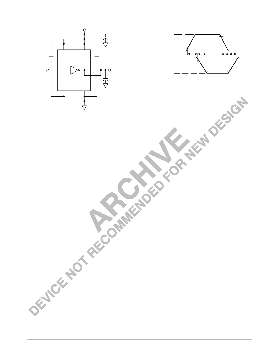
OUTPUT
VDD
INPUT
GND
NONINVERTING
4.7 V
300 mV
INVERTING
EFFECTIVE
INPUT C = 20 pF
FUNCTIONAL BLOCK DIAGRAM
NCP4421/NCP4422
Inverting/Noninverting
PDIP≠8
P SUFFIX
CASE 626
1
PIN CONNECTIONS
8
See general marking information in the device marking
section on page 8 of this data sheet.
DEVICE MARKING INFORMATION
1
5
TO≠220
T SUFFIX
CASE 314D
1
V
DD
8 V
DD
2
INPUT
3
NC
4
GND
7 OUTPUT
6 OUTPUT
5 GND
INPUT
GND
VDD
GND
OUTPUT
See detailed ordering and shipping information in the package
dimensions section on page 8 of this data sheet.
ORDERING INFORMATION
Tab is
common
to V
DD
NOTE: Duplicate pins must
both be
connected for proper operation.
NC = No connection
5≠Pin TO≠220
8≠Pin Plastic DIP
http://onsemi.com
NCP4421, NCP4422
http://onsemi.com
2
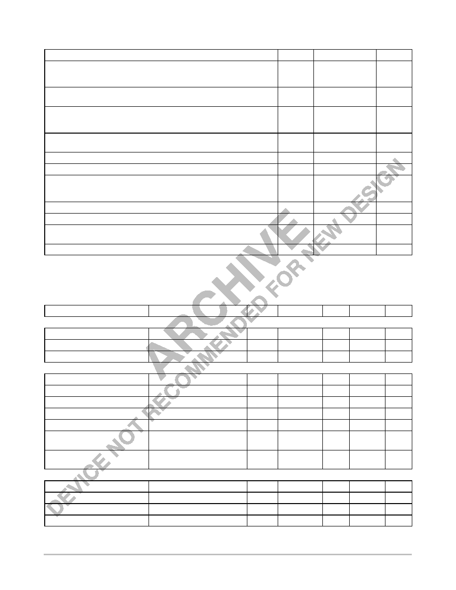
ABSOLUTE MAXIMUM RATINGS*
Rating
Symbol
Value
Unit
Power Dissipation (T
A
v
70
∞
C)
PDIP
5≠Pin TO≠220
≠
730
1.6
W
Power Dissipation (T
C
v
25
∞
C)
5≠Pin TO≠220 (With Heat Sink)
≠
12.5
W
Derating Factors (To Ambient)
PDIP
5≠Pin TO≠220
≠
8.0
12
mW/
∞
C
Thermal Impedance (To Case)
5≠Pin TO≠220 R
JC
≠
10
∞
C/W
Storage Temperature
T
stg
≠65 to +150
∞
C
Operating Temperature (Chip)
≠
150
∞
C
Operating Temperature (Ambient)
TO≠220 Version
PDIP Version
≠
0 to +70
≠40 to +85
∞
C
Lead Temperature (10 Seconds)
≠
300
∞
C
Supply Voltage
V
CC
20
V
Input Voltage
≠
V
DD
+3.0 to
GND ≠5.0
V
Input Current (V
IN
u
V
DD
)
≠
50
mA
*Static≠sensitive device. Unused devices must be stored in conductive material. Protect devices from static discharge and static fields. Stresses
above those listed under Absolute Maximum Ratings may cause permanent damage to the device. These are stress ratings only and functional
operation of the device at these or any other conditions above those indicated in the operational sections of the specifications is not implied.
Exposure to Absolute Maximum Rating Conditions for extended periods may affect device reliability.
ELECTRICAL CHARACTERISTICS
(T
A
= 25
∞
C with 4.5 V
v
V
DD
v
18 V unless otherwise specified.)
Characteristics
Test Conditions
Symbol
Min
Typ
Max
Unit
Input
Logic 1 Input Voltage
≠
V
IH
2.4
1.8
≠
V
Logic 0 Input Voltage
≠
V
IL
≠
1.3
0.8
V
Input Current
0 V
v
V
IN
v
V
DD
I
IN
≠10
≠
10
µ
A
Output
High Output Voltage
See Figure 1
V
OH
V
DD
≠ 0.025
≠
≠
V
Low Output Voltage
See Figure 1
V
OL
≠
≠
0.025
V
Output Resistance, High
V
DD
= 18 V, I
O
= 10 mA
R
O
≠
1.4
≠
Output Resistance, Low
V
DD
= 18 V, I
O
= 10 mA
R
O
≠
0.9
1.7
Peak Output Current
V
DD
= 18 V
I
PK
≠
9.0
≠
A
Continuous Output Current
10 V
v
V
DD
v
18 V, T
C
= 25
∞
(TC4421/22 CAT only)
I
DC
2.0
≠
≠
A
Latch≠Up Protection
Duty Cycle
v
2%
Withstand Reverse Current
I
REV
u
1500
t
v
300
µ
s
≠
≠
mA
Switching Time (Note 1)
Rise Time
Figure 1, C
L
= 10,000 pF
t
R
≠
60
75
nsec
Fall Time
Figure 1, C
L
= 10,000 pF
t
F
≠
60
75
nsec
Delay Time
Figure 1
t
D1
≠
30
60
nsec
Delay Time
Figure 1
t
D2
≠
33
60
nsec
1. Switching times guaranteed by design.
NCP4421, NCP4422
http://onsemi.com
3
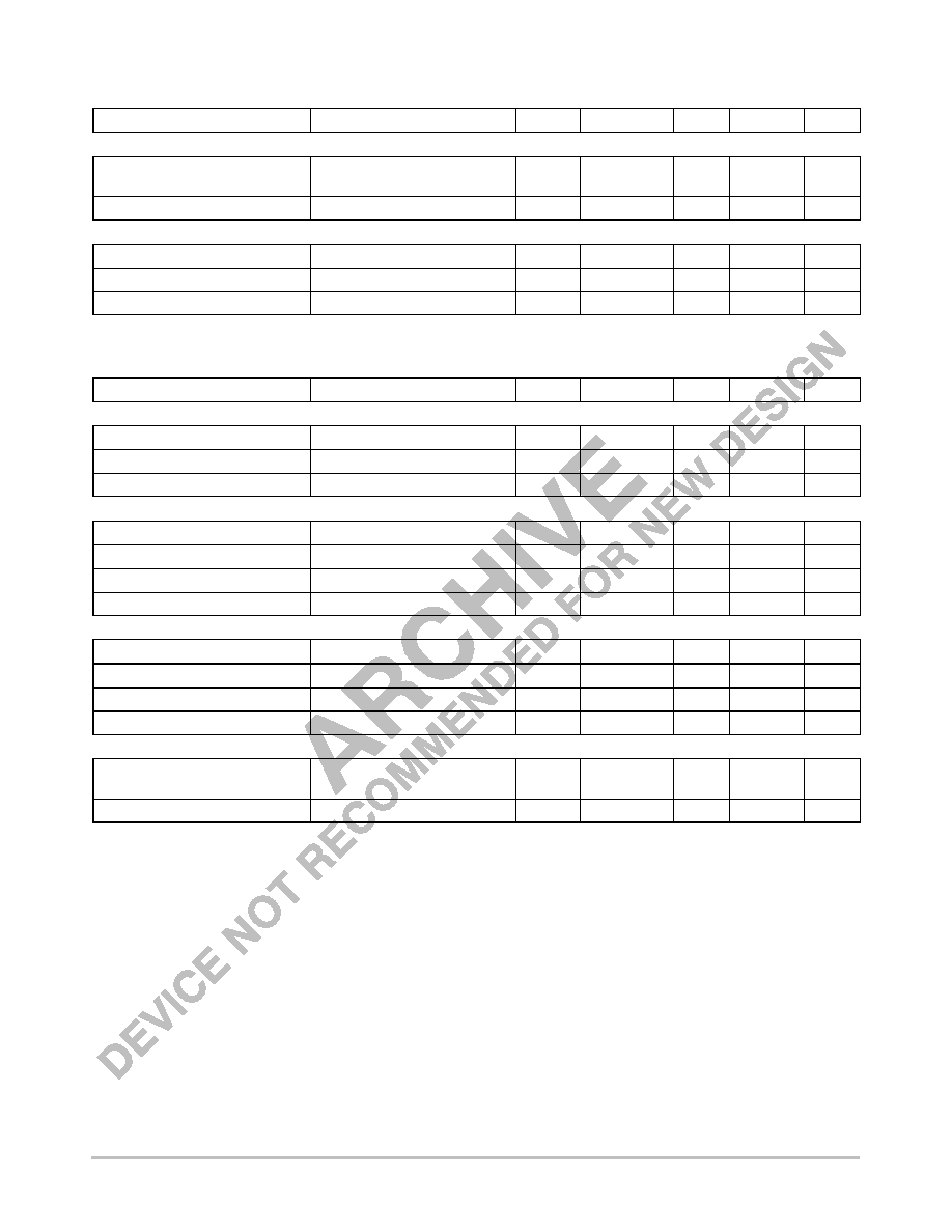
ELECTRICAL CHARACTERISTICS (continued)
(T
A
= 25
∞
C with 4.5 V
v
V
DD
v
18 V unless otherwise specified.)
Characteristics
Test Conditions
Symbol
Min
Typ
Max
Unit
Power Supply
Power Supply Current
V
IN
= 3.0 V
V
IN
= 0 V
I
S
≠
≠
0.2
55
1.5
150
mA
µ
A
Operating Input Voltage
≠
V
DD
4.5
≠
18
V
Input
Logic 1 Input Voltage
≠
V
IH
2.4
≠
≠
V
Logic 0 Input Voltage
≠
V
IL
≠
≠
0.8
V
Input Current
0 V
v
V
IN
v
V
DD
I
IN
≠10
≠
10
µ
A
ELECTRICAL CHARACTERISTICS
(Measured over operating temperature range with 4.5 V
v
V
S
v
18 V unless otherwise specified.)
Characteristics
Test Conditions
Symbol
Min
Typ
Max
Unit
Input
Logic 1 Input Voltage
≠
V
IH
2.4
≠
≠
V
Logic 0 Input Voltage
≠
V
IL
≠
≠
0.8
V
Input Current
0 V
v
V
IN
v
V
DD
I
IN
≠10
≠
10
µ
A
Output
High Output Voltage
See Figure 1
V
OH
V
DD
≠ 0.025
≠
≠
V
Low Output Voltage
See Figure 1
V
OL
≠
≠
0.025
V
Output Resistance, High
V
DD
= 18 V, I
O
= 10 mA
R
O
≠
2.4
3.6
W
Output Resistance, Low
V
DD
= 18 V, I
O
= 10 mA
R
O
≠
1.8
2.7
W
Switching Time (Note 1)
Rise Time
Figure 1, C
L
= 10,000 pF
t
R
≠
60
120
nsec
Fall Time
Figure 1, C
L
= 10,000 pF
t
F
≠
60
120
nsec
Delay Time
Figure 1
t
D1
≠
50
80
nsec
Delay Time
Figure 1
t
D2
≠
65
80
nsec
Power Supply
Power Supply Current
V
IN
= 3.0 V
V
IN
= 0 V
I
S
≠
≠
0.45
0.06
3.0
0.2
mA
Operating Input Voltage
≠
V
DD
4.5
≠
18
V
1. Switching times guaranteed by design.
NCP4421, NCP4422
http://onsemi.com
5
TYPICAL ELECTRICAL CHARACTERISTICS
90
80
60
70
50
40
30
35
30
25
40
45
50
120
160
100
140
80
180
4
140
200
12
120
180
14
10
8
16
V
DD
t
RISE
(ns)
100
160
0
6
V
DD
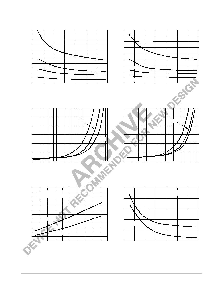
Figure 2. Rise Time vs. Supply Voltage
Figure 3. Fall Time vs. Supply Voltage
t
FA
L
L
(ns)
100
300
250
200
150
1 k
100
50
0
10 k
100 k
Figure 4. Rise Time vs. Capacitive Load
C
LOAD
(pF)
Figure 5. Fall Time vs. Capacitive Load
C
LOAD
(pF)
t
FA
L
L
(ns)
t
RISE
(ns)
Figure 6. Rise and Fall Times vs. Temperature
T
A
(
∞
C)
Figure 7. Propagation Delay vs. Supply
Voltage
V
DD
TIME
(ns)
TIME (ns)
220
18
40
0
≠40
80
120
4
12
14
10
8
16
6
18
4
12
14
10
8
16
6
18
80
60
40
20
60
40
20
0
100
300
250
200
150
1 k
100
50
0
10 k
100 k
4700 pF
1000 pF
22000 pF
10000 pF
4700 pF
10000 pF
1000 pF
22000 pF
5 V
5 V
10 V
10 V
15 V
15 V
C
LOAD
= 10000 pF
V
DD
= 15 V
t
RISE
t
FALL
C
LOAD
= 1000 pF
t
D2
t
D1