Äîêóìåíòàöèÿ è îïèñàíèÿ www.docs.chipfind.ru
©
Semiconductor Components Industries, LLC, 2004
July, 2004 - Rev. 4
1
Publication Order Number:
NCP5007/D
NCP5007
Compact Backlight LED
Boost Driver
The NCP5007 is a high efficiency boost converter operating in a
current control loop, based on a PFM mode, to drive White LEDs. The
current mode regulation allows a uniform brightness of the LEDs. The
chip has been optimized for small ceramic capacitors and is capable of
supplying up to 1.0 W output power.
Features
·
Inductor Based Converter brings High Efficiency
·
Constant Output Current Regulation
·
2.7 to 5.5 V Input Voltage Range
·
V
out
to 22 V Output Compliance Allows up to 5 LEDs to be Driven
in Series which Provides Automatic LED Current Matching
·
Built-in Output Overvoltage Protection
·
0.3
mA Standby Quiescent Current
·
Includes Dimming Function (PWM)
·
Enable Function Driven Directly from Low Battery Voltage Source
·
Thermal Shutdown Protection
·
All Pins are Fully ESD Protected
·
Low EMI Radiation
·
Pb-Free Package is Available
Typical Applications
·
LED Display Back Light Control
·
High Efficiency Step Up Converter
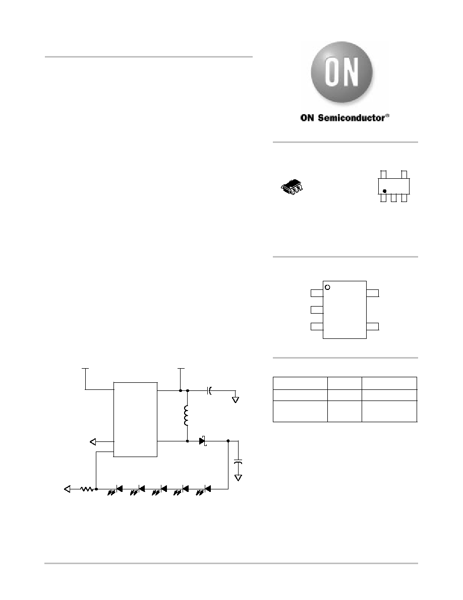
Figure 1. Typical Application
GND
EN
2
4
5
V
out
V
bat
NCP5007
L1
22
m
H
V
bat
C1
4.7
m
F
GND
D6
D5
D4
D3
U1
3
D2
V
bat
GND
1
GND
R1
5.6
W
D1
MBR0530
GND
C2
1.0
m
F
FB
http://onsemi.com
TSOP-5
(SOT23-5, SCR59-5)
SN SUFFIX
CASE 483
MARKING
DIAGRAM
DCL = Device Code
Y
= Year
W
= Work Week
1
5
DCLYW
5
4
1
2
3
PIN CONNECTIONS
FB
GND
EN
V
bat
V
out
(Top View)
1
5
Device
Package
Shipping
ORDERING INFORMATION
NCP5007SNT1
TSOP-5
3000 Tape & Reel
NCP5007SNT1G
TSOP-5
(Pb-Free)
3000 Tape & Reel
For information on tape and reel specifications,
including part orientation and tape sizes, please
refer to our Tape and Reel Packaging Specifications
Brochure, BRD8011/D.
NCP5007
http://onsemi.com
2
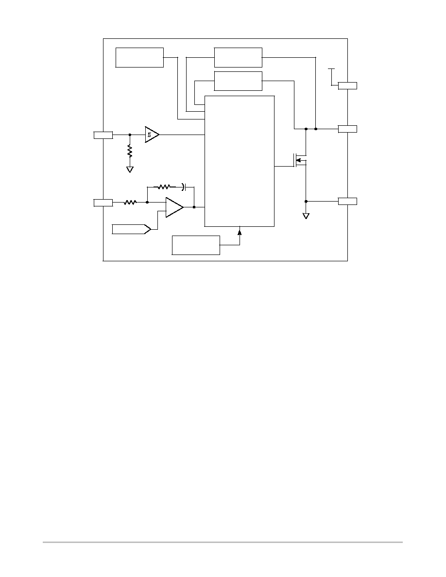
Figure 2. Block Diagram
V
bat
V
bat
CONTROLLER
GND
Q1
+200 mV
100 k
EN
GND
GND
Thermal
Shutdown
3
Current Sense
Vsense
2
5
V
out
4
Band Gap
+
-
1
FB
300 k

NCP5007
http://onsemi.com
3
PIN FUNCTION DESCRIPTION
Pin
Symbol
Type
Description
1
FB
ANALOG
INPUT
This pin provides the output current range adjustment by means of a sense resistor connected
to the analog control or with a PWM control. The dimming function can be achieved by applying
a PWM voltage technique to this pin (see Figure 29). The current output tolerance depends
upon the accuracy of this resistor. Using a
"
5% metal film resistor, or better, yields good output
current accuracy. Note: A built-in comparator switches OFF the DC-DC converter if the voltage
sensed across this pin and ground is higher than 700 mV typical.
2
GND
POWER
This pin is the system ground for the NCP5007 and carries both the power and the analog
signals. High quality ground must be provided to avoid spikes and/or uncontrolled operation.
Care must be observed to avoid high-density current flow in a limited PCB copper track so a
robust ground plane connection is recommended.
3
EN
DIGITAL
INPUT
This is an Active-High logic input which enables the boost converter. The built-in pulldown
resistor disables the device when the EN pin is left open. Note the logic switching level of this
input has been optimized to allow it to be driven from standard or 1.8 V CMOS logic levels.
The LED brightness can be controlled by applying a pulse width modulated signal to the enable
pin (see Figure 30).
4
V
out
POWER
This pin is the power side of the external inductor and must be connected to the external
Schottky diode. It provides the output current to the load. Since the boost converter operates in
a current loop mode, the output voltage can range up to +22 V but shall not exceed this limit.
However, if the voltage on this pin is higher than the OVP threshold (Over Voltage Protection)
the device enters a shutdown mode. To restart the chip, one must either apply a low to high logic
signal to the EN pin, or switch off the V
bat
supply.
A capacitor must be used on V
out
to avoid false triggering of the OVP (Overvoltage Protect)
circuit. This capacitor filters the noise created by the fast switching transients. In order to limit
the inrush current and still have acceptable startup time the capacitor value should range
between 1.0
m
F and 8.2
m
F max. To achieve high efficiency this capacitor should be ceramic
(ESR
t
100 m
W
).
Care must be observed to avoid EMI through the PCB copper tracks connected to this pin.
5
V
bat
POWER
The external voltage supply is connected to this pin. A high quality reservoir capacitor must be
connected across pin 5 and Ground to achieve the specified output voltage parameters. A
4.7
m
F/6.3 V, low ESR capacitor must be connected as close as possible across pin 5 and
ground pin 2. The X5R or X7R ceramic MURATA types are recommended.
The return side of the external inductor shall be connected to this pin. Typical application will
use a 22
m
H, size 1210, to handle the 10 to 100 mA output current range. When the desired
output current is above 20 mA, the inductor shall have an ESR
v
1.5
W
to achieve good
efficiency over the V
bat
range
.
The output current tolerance can be improved by using a larger
inductor value.
NCP5007
http://onsemi.com
4
MAXIMUM RATINGS
Rating
Symbol
Value
Unit
Power Supply
V
bat
6.0
V
Output Power Supply Voltage Compliance
V
out
28
V
Digital Input Voltage
Digital Input Current
EN
-0.3
v
V
in
v
V
bat
+0.3
1.0
V
mA
ESD Capability (Note 1)
Human Body Model (HBM)
Machine Model (MM)
V
ESD
2.0
200
kV
V
TSOP5 Package
Power Dissipation @ T
A
= +85
°
C (Note 2)
Thermal Resistance, Junction-to-Air
P
D
R
q
JA
160
250
mW
°
C/W
Operating Ambient Temperature Range
T
A
-25 to +85
°
C
Operating Junction Temperature Range
T
J
-25 to +125
°
C
Maximum Junction Temperature
T
Jmax
+150
°
C
Storage Temperature Range
T
stg
-65 to +150
°
C
Maximum ratings are those values beyond which device damage can occur. Maximum ratings applied to the device are individual stress limit
values (not normal operating conditions) and are not valid simultaneously. If these limits are exceeded, device functional operation is not implied,
damage may occur and reliability may be affected.
1. This device series contains ESD protection and exceeds the following tests:
Human Body Model (HBM)
"
2.0 kV per JEDEC standard: JESD22-A114
Machine Model (MM)
"
200 V per JEDEC standard: JESD22-A115
2. The maximum package power dissipation limit must not be exceeded.
3. Latchup current maximum rating:
"
100 mA per JEDEC standard: JESD78.
4. Moisture Sensivity Level (MSL): 1 per IPC/JEDEC standard: J-STD-020A.
POWER SUPPLY SECTION
(Typical values are referenced to T
a
= +25
°
C, Min & Max values are referenced -25
°
C to +85
°
C ambient
temperature, unless otherwise noted.)
Rating
Pin
Symbol
Min
Typ
Max
Unit
Power Supply
4
V
bat
2.7
-
5.5
V
Output Load Voltage Compliance
5
V
out
22
24.5
-
V
Continuous DC Current in the Load
@ V
out
= 3
LED, L = 22
m
H, ESR < 1.5
W
, V
bat
= 3.6 V
5
I
out
50
-
-
mA
Standby Current @ I
out
= 0 mA, EN = L, V
bat
= 3.6 V
4
I
stdb
-
0.45
-
m
A
Standby Current @ I
out
= 0 mA, EN = L, V
bat
= 5.5 V
4
I
stdb
-
1.0
3.0
m
A
Inductor Discharging Time @ V
bat
= 3.6 V, L = 22
m
H, 3
LED,
I
out
= 10 mA
4
Toffmax
-
320
-
ns
Thermal Shutdown Protection
-
T
SD
-
160
-
°
C
Thermal Shutdown Protection Hysteresis
-
T
SDH
-
30
-
°
C
NCP5007
http://onsemi.com
5
ANALOG SECTION
(Typical values are referenced to T
a
= +25
°
C, Min & Max values are referenced -25
°
C to +85
°
C ambient
temperature, unless otherwise noted.)
Rating
Pin
Symbol
Min
Typ
Max
Unit
High Level Input Voltage
Low Level Input Voltage
1
EN
1.3
-
-
-
-
0.4
V
EN Pull Down Resistor
1
R
EN
-
100
-
k
W
Feedback Voltage Threshold
4
FB
170
200
230
mV
Output Current Stabilizes @ 5% time delay following a
DC-DC startup @ V
bat
= 3.6 V, L = 22
m
H, I
out
= 20 mA
5
I
outdly
-
100
-
m
s
Internal Switch ON Resistor @ T
amb
= +25
°
C
5
QR
DSON
-
1.7
-
W
5. The overall tolerance depends upon the accuracy of the external resistor.
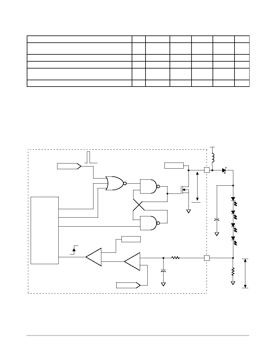
THEORY OF OPERATION
The DC-DC converter is designed to supply a constant
current to the external load, the circuit being powered from
a standard battery supply. Since the regulation is made by
means of a current loop, the output voltage will vary
depending upon the dynamic impedance presented by the
load.
Considering a high intensity LED, the output voltage can
range from a low of 6.4 V (two LED in series biased with a
low current), up to 22 V, the maximum the chip can sustain
continuously. The basic DC-DC structure is depicted in
Figure 3.
With a 22 V operating voltage capability, the power
device Q1 can accommodate a high voltage source without
any leakage current degradation.
POR
LOGIC
CONTROL
TIME_OUT
ZERO_CROSSING
RESET
GND
Vdsense
Q1
Vds
L1
22
m
H
V
bat
D1
C2
D5
D4
D3
D2
GND
Vs
R2
xR
GND
R1
C2
+
-
GND
Vref
V(Ipeak)
+
-
Vdsense
Figure 3. Basic DC-DC Converter Structure
4
1
1.0
m
F
NCP5007
http://onsemi.com
6
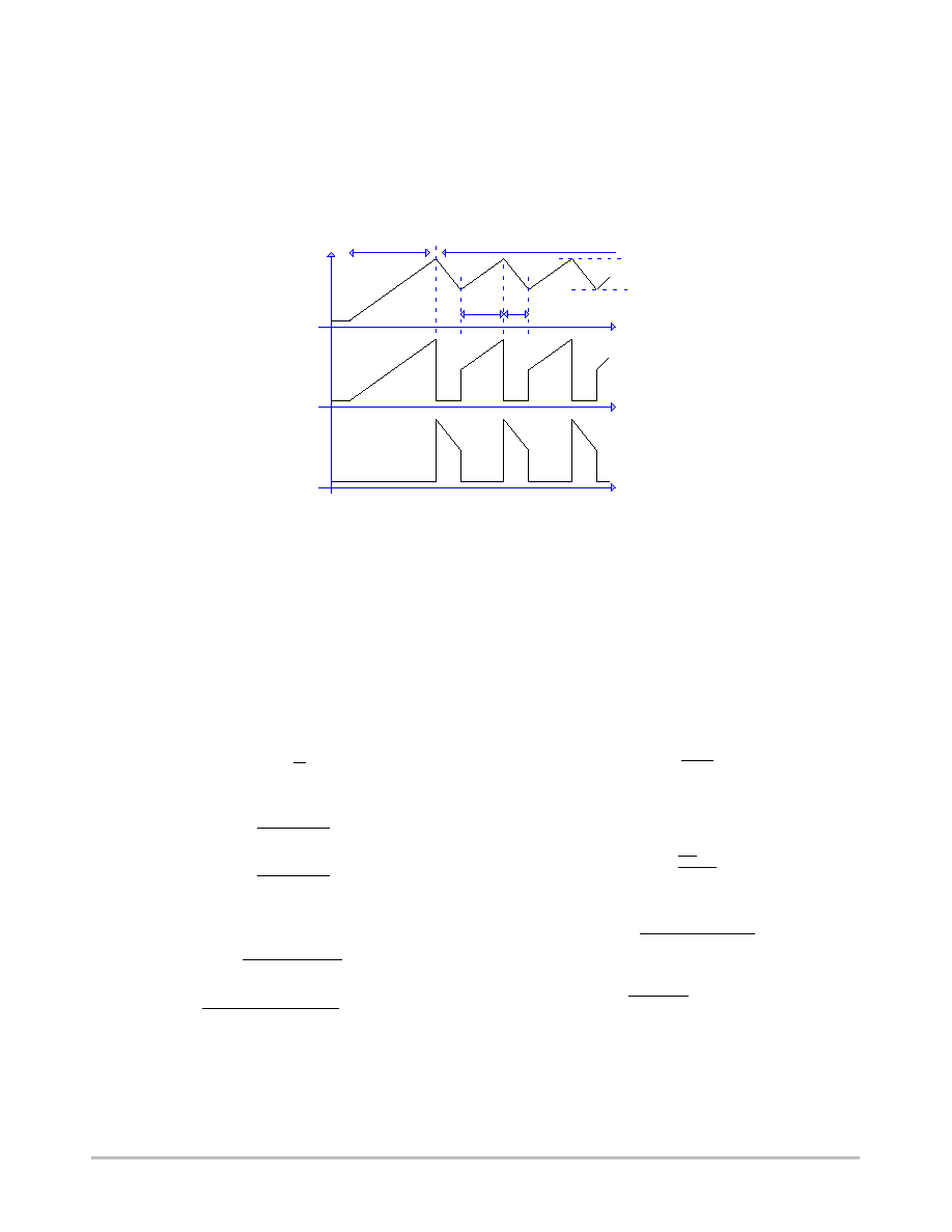
Basically, the chip operates with two cycles:
Cycle #1 : time t1, the energy is stored into the inductor
Cycle #2 : time t2, the energy is dumped to the load
The POR signal sets the flip-flop and the first cycle takes
place. When the current hits the peak value, defined by the
error amplifier associated with the loop regulation, the
flip-flop resets, the NMOS is deactivated and the current is
dumped into the load. Since the timing is application
dependent, the internal timer limits the Toff cycle to 320 ns
(typical), making sure the system operates in a continuous
mode to maximize the energy transfer.
Figure 4. Basic DC-DC Operation
First Startup
Normal Operation
I
L
0 mA
Ids
0 mA
Io
0 mA
Iv
Ipeak
t
t
t
t1
t2
Based on the data sheet, the current flowing into the
inductor is bounded by two limits:
·
Ipeak Value: Internally fixed to 350 mA typical
·
Iv Value: Limited by the fixed Toff time built in the
chip (320 ns typical)
The system operates in a continuous mode as depicted in
Figure 4 and t
1
& t
2
times can be derived from basic
equations. (Note: The equations are for theoretical analysis
only, they do not include the losses.)
E
+
L *
di
dt
(eq. 1)
Let E = V
bat
, then:
t1
+
(Ip
*
Iv) * L
Vbat
(eq. 2)
t2
+
(Ip
*
Iv) * L
Vo
*
Vbat
(eq. 3)
Since t
2
= 320 ns typical and Vo = 22 V maximum, then
(assuming a typical V
bat
= 3.0 V):
D
I
+
t2 * (Vo
*
Vbat)
L
(eq. 4)
D
Imax
+
320e
*
9 * (22
*
3.0)
22e
*
6
+
276 mA
Of course, from a practical stand point, the inductor must
be sized to cope with the peak current present in the circuit
to avoid saturation of the core. On top of that, the ferrite
material shall be capable to operate at high frequency
(1.0 MHz) to minimize the Foucault's losses developed
during the cycles.
The operating frequency can be derived from the
electrical parameters. Let V = Vo - V
bat
, rearranging
Equation 1:
ton
+
dI * L
E
(eq. 5)
Since toff is nearly constant (according to the 320 ns
typical time), the dI is constant for a given load and
inductance value. Rearranging Equation 5 yields:
ton
+
V*dt
L
* L
E
(eq. 6)
Let E = V
bat
, and Vopk = output peak voltage, then:
ton
+
(Vopk
*
Vbat) * dt
Vbat
(eq. 7)
Finally, the operating frequency is:
F
+
1
ton
)
toff
(eq. 8)
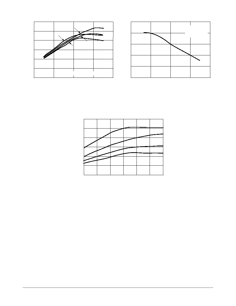
The output power supplied by the NCP5007 is limited to
one watt: Figure 5 shows the maximum power that can be
delivered by the chip as a function of the input voltage.
NCP5007
http://onsemi.com
7
1200
6
400
5
3
P
out
(mW)
0
V
bat
(V)
200
800
1000
600
2
4
P
out
= f(V
bat
) @ R
sense
= 2.0
W
2 LED
3 LED
5 LED
4 LED
120
40
I
out
(mA)
0
V
bat
(V)
20
80
100
60
3.0
4.0
5.0
2.5
3.5
4.5
5.5
Figure 5. Maximum Output Power as a Function of
the Battery Supply Voltage
Figure 6. Typical Inductor Peak Current as a
Function of V
bat
Voltage
Figure 7. Maximum Output Current as a Function of V
bat
350
4
3
2
Ipeak
(mA)
150
400
V
bat
(V)
200
300
5
250
6
L = 22
µ
H
R
sense
= 10
W
T
A
= +25
°
C
Test conditions: 5 LEDs in series, steady state operation
Test conditions: L = 22
m
H, Rsense = 2.0
W
, Tamb = +25
°
C
2 LED
3 LED
4 LED
5 LED
NCP5007
http://onsemi.com
8
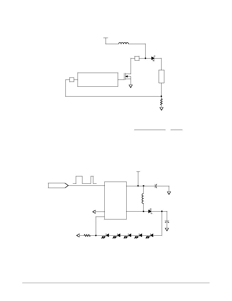
Output Current Range Set-Up
The current regulation is achieved by means of an external sense resistor connected in series with the LED string.
CONTROLLER
GND
1
FB
GND
4
V
out
D1
Load
Q1
Figure 8. Output Current Feedback
V
bat
L1
22
m
H
R1
x
W
The current flowing through the LED creates a voltage
drop across the sense resistor R1. The voltage drop is
constantly monitored internally, and maximum peak current
allowed in the inductor is set accordingly in order to keep
constant this voltage drop (and thus the current flowing
through the LED). For example, should one need a 10 mA
output current, the sense resistor should be sized according
to the following equation:
R1
+
Feedback Threshold
Iout
+
200 mV
10 mA
+
20
W
(eq. 9)
A standard 5% tolerance resistor, 22
W SMD device,
yields 9.09 mA, good enough to fulfill the back light
demand. The typical application schematic diagram is
provided in Figure 9.
Figure 9. Basic Schematic Diagram
GND
EN
2
4
5
V
out
V
bat
NCP5007
L1
22
m
H
V
bat
C1
4.7
m
F
GND
D6
D5
D4
D3
U1
3
D2
GND
1
GND
R1
22
W
D1
MBR0530
GND
C2
1.0
m
F
FB
Pulse
LED
LED
LED
LED
LED
NCP5007
http://onsemi.com
9
Output Load Drive
In order to take advantage of the built-in Boost
capabilities, one shall operate the NCP5007 in the
continuous
output current mode. Such a mode is achieved by
using and external reservoir capacitor (see Table 1) across
the LED.
At this point, the peak current flowing into the LED diodes
shall be within the maximum ratings specified for these
devices. Of course, pulsed operation can be achieved, thanks
to the EN signal pin 3, to force high current into the LED
when necessary.
The Schottky diode D1, associated with capacitor C2 (see
Figure 9), provides a rectification and filtering function.
When a pulse-operating mode is required:
·
A PWM mode control can be used to adjust the output
current range by means of a resistor and a capacitor
connected across FB pin. On the other hand, the
Schottky diode can be removed and replaced by at least
one LED diode, keeping in mind such LED shall
sustain the large pulsed peak current during the
operation.
TYPICAL OPERATING CHARACTERISTICS
0
10
20
30
40
50
60
70
80
90
100
2.50
3.00
3.50
4.00
4.50
5.00
5.50
Vbat (V)
EFFICIENCY
(%)
5 LED/10 mA
3 LED/10 mA
4 LED/10 mA
2 LED/10 mA
0
10
20
30
40
50
60
70
80
90
100
2.50
3.00
3.50
4.00
4.50
5.00
5.50
Vbat (V)
EFFICIENCY
(%)
5 LED/4 mA
3 LED/4 mA
4 LED/4 mA
2 LED/4 mA
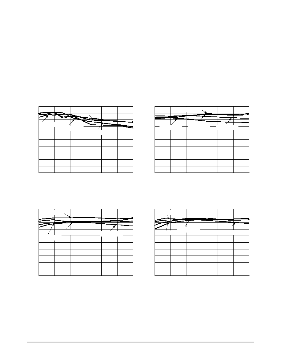
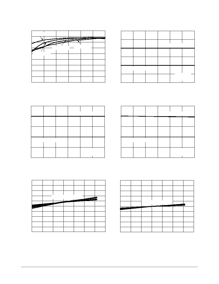
Figure 10. Overall Efficiency vs. Power Supply -
I
out
= 4.0 mA, L = 22
m
H
Figure 11. Overall Efficiency vs. Power Supply -
I
out
= 10 mA, L = 22
m
H
0
10
20
30
40
50
60
70
80
90
100
2.50
3.00
3.50
4.00
4.50
5.00
5.50
Vbat (V)
EFFICIENCY
(%)
5 LED/20 mA
3 LED/20 mA
4 LED/20 mA
2 LED/20 mA
0
10
20
30
40
50
60
70
80
90
100
2.50
3.00
3.50
4.00
4.50
5.00
5.50
Vbat (V)
EFFICIENCY
(%)
5 LED/15 mA
3 LED/15 mA
4 LED/15 mA
2 LED/15 mA
Figure 12. Overall Efficiency vs. Power Supply -
I
out
= 15 mA, L = 22
m
H
Figure 13. Overall Efficiency vs. Power Supply -
I
out
= 20 mA, L = 22
m
H
NCP5007
http://onsemi.com
10
Figure 14. Overall Efficiency vs. Power Supply -
I
out
= 40 mA, L = 22
m
H
Figure 15. Current Variation vs. Power Supply with
3 Series LED's
Figure 16. Current Variation vs. Power Supply with
4 Series LED's
Figure 17. Current Variation vs. Power Supply with
5 Series LED's
Figure 18. Feedback Voltage Stability
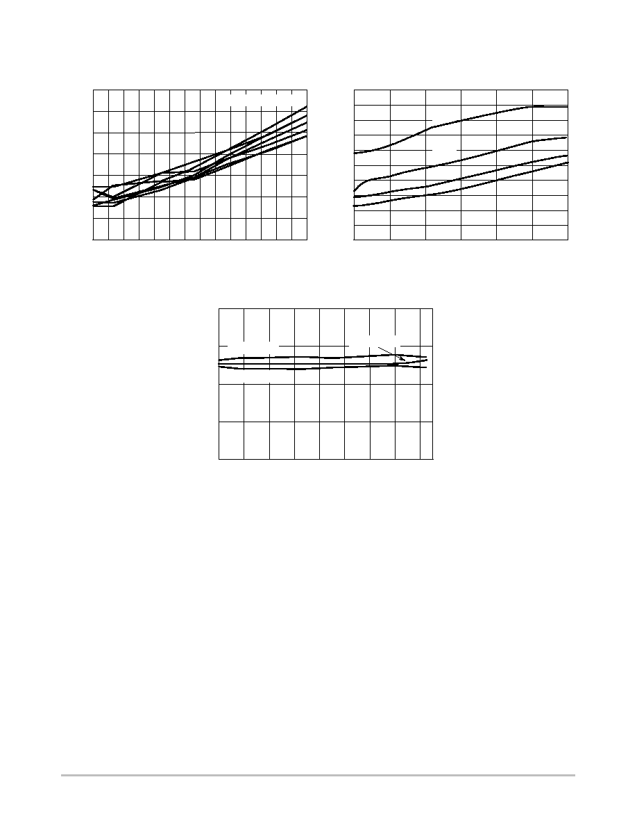
TYPICAL OPERATING CHARACTERISTICS
EFFICIENCY
(%)
V
bat
(V)
205
200
FEEDBACK VOL
T
AGE (mV)
195
TEMPERATURE (
°
C)
199
202
203
201
0
20
100
198
197
196
-40
40
-20
60
80
204
5
0
FEEDBACK V
ARIA
TION (%)
-5
TEMPERATURE (
°
C)
-1
2
3
1
0
20
100
-2
-3
-4
-40
40
-20
60
80
4
V
bat
= 3.1V thru 5.5V
30
15
2.5
I
OUT
(mA)
0
V
BAT
(V)
25
3.0
5.0
10
4.0
4.5
I
OUT
= 10 mA Nom
L = 22
m
H
T
A
= 25
°
C
3.5
V
bat
= 3.1 V thru 5.5 V
(All curve conditions: L = 22
m
H, Cin = 4.7
m
F, C
out
= 1.0
m
F, Typical curve @ T
a
= +25
°
C)
Figure 19. Feedback Voltage Variation
0
10
20
30
40
50
60
70
80
90
100
2.50
3.00
3.50
4.00
4.50
5.00
5.50
5 LED/40 mA
3 LED/40 mA
4 LED/40 mA
2 LED/40 mA
5.5
20
5
I
OUT
= 20 mA Nom
25
15
2.5
I
OUT
(mA)
0
V
BAT
(V)
3.0
5.0
10
4.0
4.5
I
OUT
= 10 mA Nom
L = 22
m
H
T
A
= 25
°
C
3.5
5.5
20
5
I
OUT
= 20 mA Nom
25
15
2.5
I
OUT
(mA)
0
V
BAT
(V)
3.0
5.0
10
4.0
4.5
I
OUT
= 10 mA Nom
L = 22
m
H
T
A
= 25
°
C
3.5
5.5
20
5
I
OUT
= 20 mA Nom
NCP5007
http://onsemi.com
11
4 LED
5 LED
Figure 20. Standby Current
Figure 21. Typical Operating Frequency
Figure 22. Overvoltage Protection
TYPICAL OPERATING CHARACTERISTICS
1.4
2.7
IStby (
µ
A)
0.0
V
bat
, BATTERY VOLTAGE (V)
0.6
1.0
0.8
5.5
0.4
0.2
1.2
-40
°
C thru 125
°
C
3.3
3.9
4.5
5.1
26
24
-40
OVER VOL
T
AGE PROTECTION (V)
22
TEMPERATURE(
°
C)
25
0
100
23
40
80
V
bat
= 5.5V
V
bat
= 2.7V
V
bat
= 3.6V
20
130
(All curve conditions: L = 22
m
H, Cin = 4.7
m
F, C
out
= 1.0
m
F, Typical curve @ T
a
= +25
°
C)
0
0.5
1.0
1.5
2.0
2.5
2.5
3.0
3.5
4.0
4.5
5.0
5.5
2 LED
F (mHz)
V
bat
(V)
3 LED
-20
60
120
NCP5007
http://onsemi.com
12
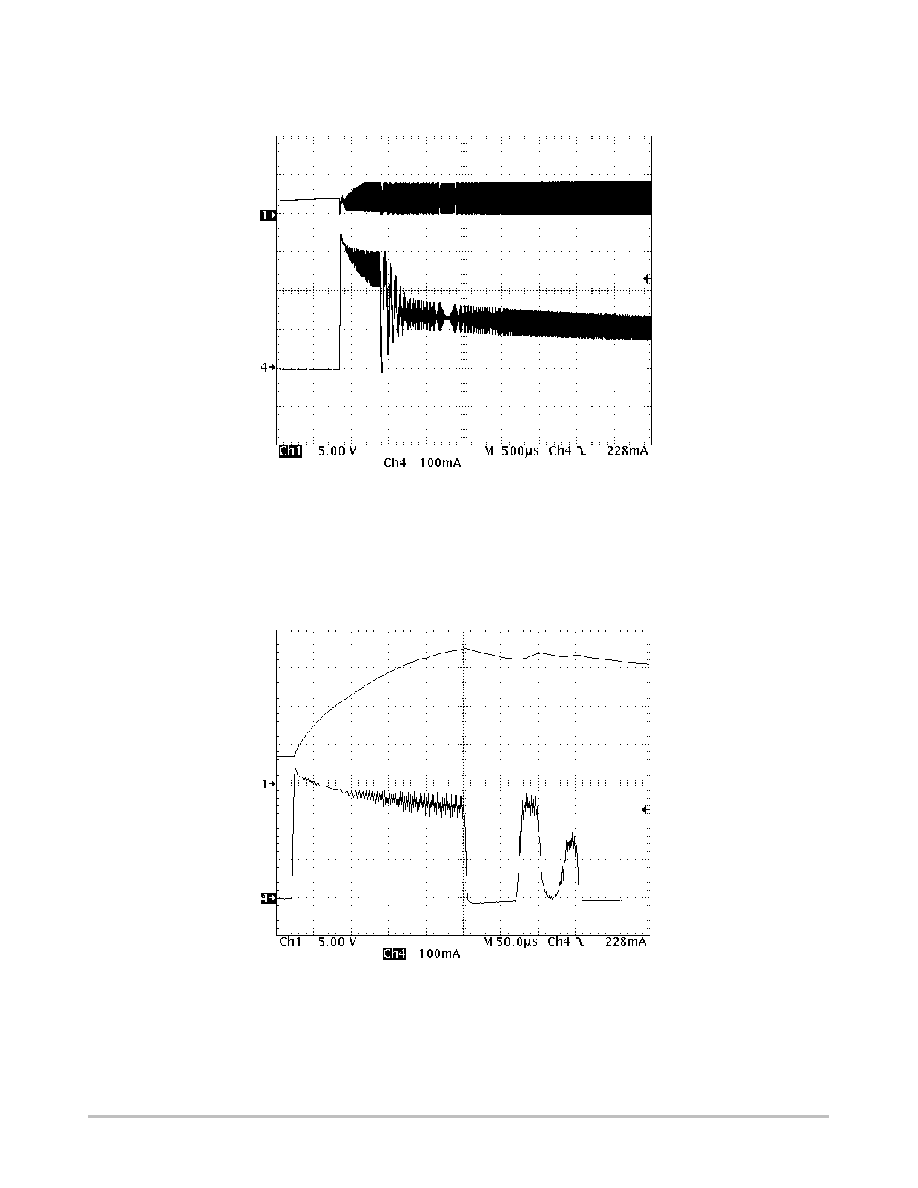
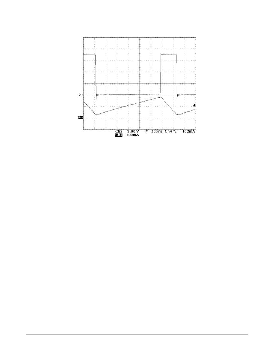
Figure 23. Typical Power Up Response
Figure 24. Typical Startup Inductor Current and Output Voltage
TYPICAL OPERATING WAVEFORMS
Conditions: V
bat
= 3.6 V, L
out
= 22
m
H, 5 LED, I
out
= 15 mA
Conditions: V
bat
= 3.6 V, L
out
= 22
m
H, 5 LED, I
out
= 15 mA
Inductor
Current
V
out
V
out
Inductor
Current
NCP5007
http://onsemi.com
13
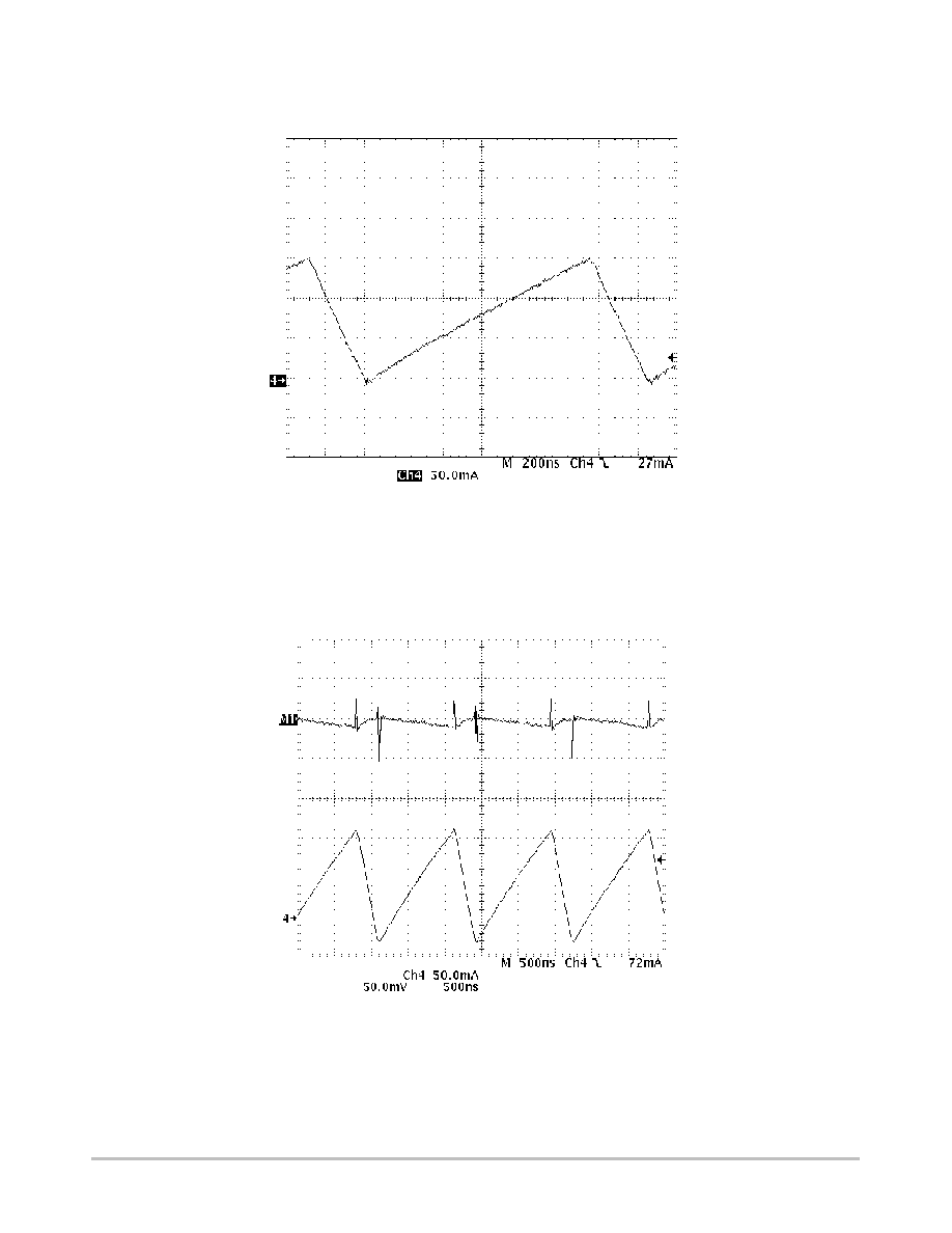
Figure 25. Typical Inductor Current
Figure 26. Typical Output Voltage Ripple
TYPICAL OPERATING WAVEFORMS
Conditions: V
bat
= 3.6 V, L
out
= 22
m
H, 5 LED, I
out
= 15 mA
Conditions: V
bat
= 3.6 V, L
out
= 22
m
H, 5 LED, I
out
= 15 mA
Inductor
Current
Inductor
Current
V
out
Ripple
50 mV/div
NCP5007
http://onsemi.com
14
Figure 27. Typical Output Peak Voltage
TYPICAL OPERATING WAVEFORMS
Test Conditions: L = 22
m
H, I
out
= 15 mA, V
bat
= 3.6 V, Ambient Temperature, LED = 5
Output Voltage
Inductor Current
NCP5007
http://onsemi.com
15
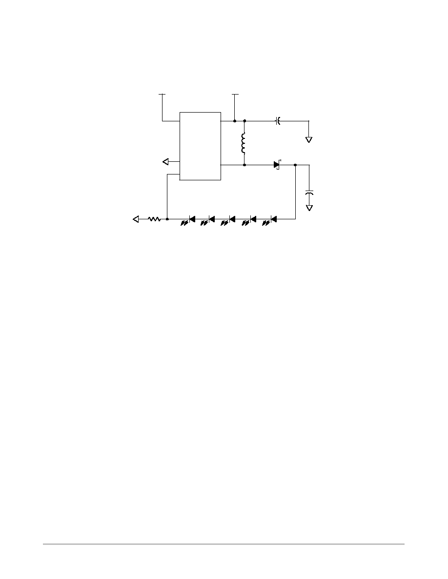
TYPICAL APPLICATIONS CIRCUITS
Standard Feedback
The standard feedback provides constant current to the
LEDs, independently of the V
bat
supply and number of
LEDs in series. Figure 28 depicts a typical application to
supply 13 mA to the load.
Figure 28. Basic DC Current Mode Operation with
Analog Feedback
EN
4
5
V
out
V
bat
R1
NCP5007
L1
22
m
H
V
bat
C1
4.7
m
F
D6
D5
D4
D3
U1
3
D2
V
bat
2
GND
GND
FB
1
D1
MBR0530
15
W
GND
GND
C2
1.0
m
F
LED
LED
LED
LED
LED
GND
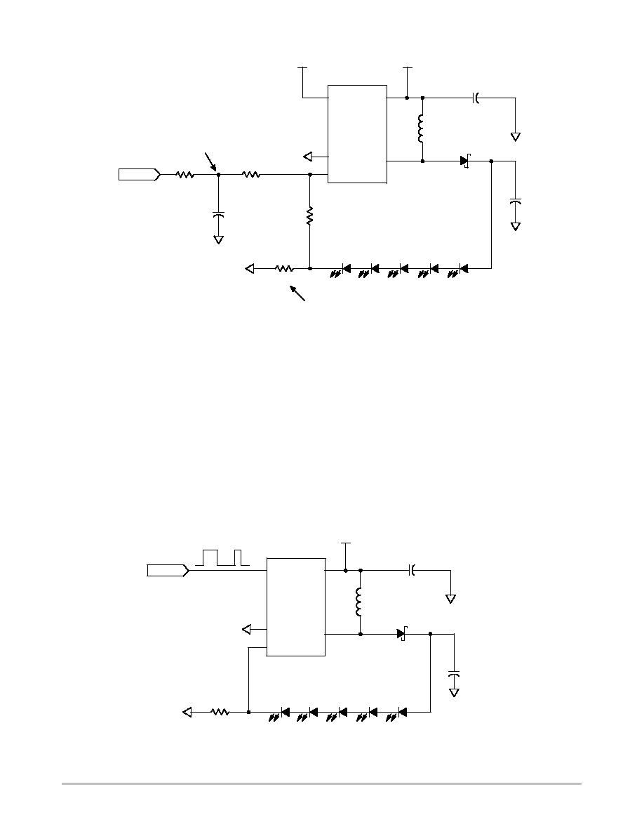
PWM Operation
The analog feedback pin 1 provides a way to dim the LED
by means of an external PWM signal as depicted in
Figure 29. Taking advantage of the high internal impedance
presented by the FB pin, one can set up a simple R/C network
to accommodate such a dimming function. Two modes of
operation can be considered:
·
Pulsed mode, with no filtering
·
Averaged mode with filtering capacitor
Although the pulsed mode will provide a good dimming
function, it will yield high switching transients which are
difficult to filter out in the control loop. As such this first
approach is not recommended. The output current depends
upon the duty cycle of the signal presented to the node pin 1:
this is very similar to the digital control shown in Figure 30.
The average mode yields a noise-free operation since the
converter operates continuously, together with a very good
dimming function. The cost is an extra resistor and one extra
capacitor, both being low cost parts.
NCP5007
http://onsemi.com
16
Figure 29. Basic DC Current Mode Operation with PWM Control
EN
4
5
V
out
V
bat
R1
NCP5007
L1
22
m
H
V
bat
C1
4.7
m
F
D6
D5
D4
D3
U1
3
D2
V
bat
2
GND
GND
FB
1
D1
MBR0530
10
W
GND
GND
C2
1.0
m
F
LED
LED
LED
LED
LED
R4
5.6 k
R3
10 k
GND
C3
100 nF
Sense Resistor
R2
150 k
PWM
Average Network
NOTE: RC filter R2 and C3 is optional (see text)
GND
To implement such a function, lets consider the feedback
input as an operational amplifier with a high impedance input
(reference schematic Figure 29). The analog loop will keep
going to balance the current flowing through the sense
resistor R1 until the feedback voltage is 200 mV. An extra
resistor (R4) isolates the FB node from low resistance to
ground, making possible to add an external voltage to this pin.
The time constant R2/C3 generates the voltage across C3,
added to the node pin 1, while R2/R3/R4/R1/C3 create the
discharge time constant. In order to minimize the pick up
noise at FB node, the resistors shall have relative medium
value, preferably well below 1.0 M
W. Consequently, let
R2 = 150 k, R3 = 10 k and R4 = 5.6 k. In addition, the
feedback delay to control the luminosity of the LED shall be
acceptable by the user, 10 ms or less being a good
compromise. The time constant can now be calculated based
on a 400 mV offset voltage at the C3/R2/R3 node to force
zero current to the LED. Assuming the PWM signal comes
from a standard gate powered by a 3.0 V supply, running at
5.0 kHz, then full dimming of the LED can be achieved with
a 95% span of the Duty Cycle signal.
Digital Control
An alternative method of controlling the luminosity of the
LEDs is to apply a PWM signal to the EN pin (see
Figure 30). The output current depends upon the Duty
Cycle, but care must be observed as the DC-DC converter
is continuously pulsed ON/OFF and noise is likely to be
generated.
Figure 30. Typical Semi-Pulsed Mode of Operation
EN
4
5
V
out
V
bat
R1
NCP5007
L1
22
m
H
V
bat
C1
4.7
m
F
GND
D6
D5
D4
D3
U1
3
D2
2
GND
GND
FB
1
D1
MBR0530
5.6
W
GND
GND
Pulse
C2
1.0
m
F
NOTE: Pulse width and frequency depends upon the application constraints.
NCP5007
http://onsemi.com
17
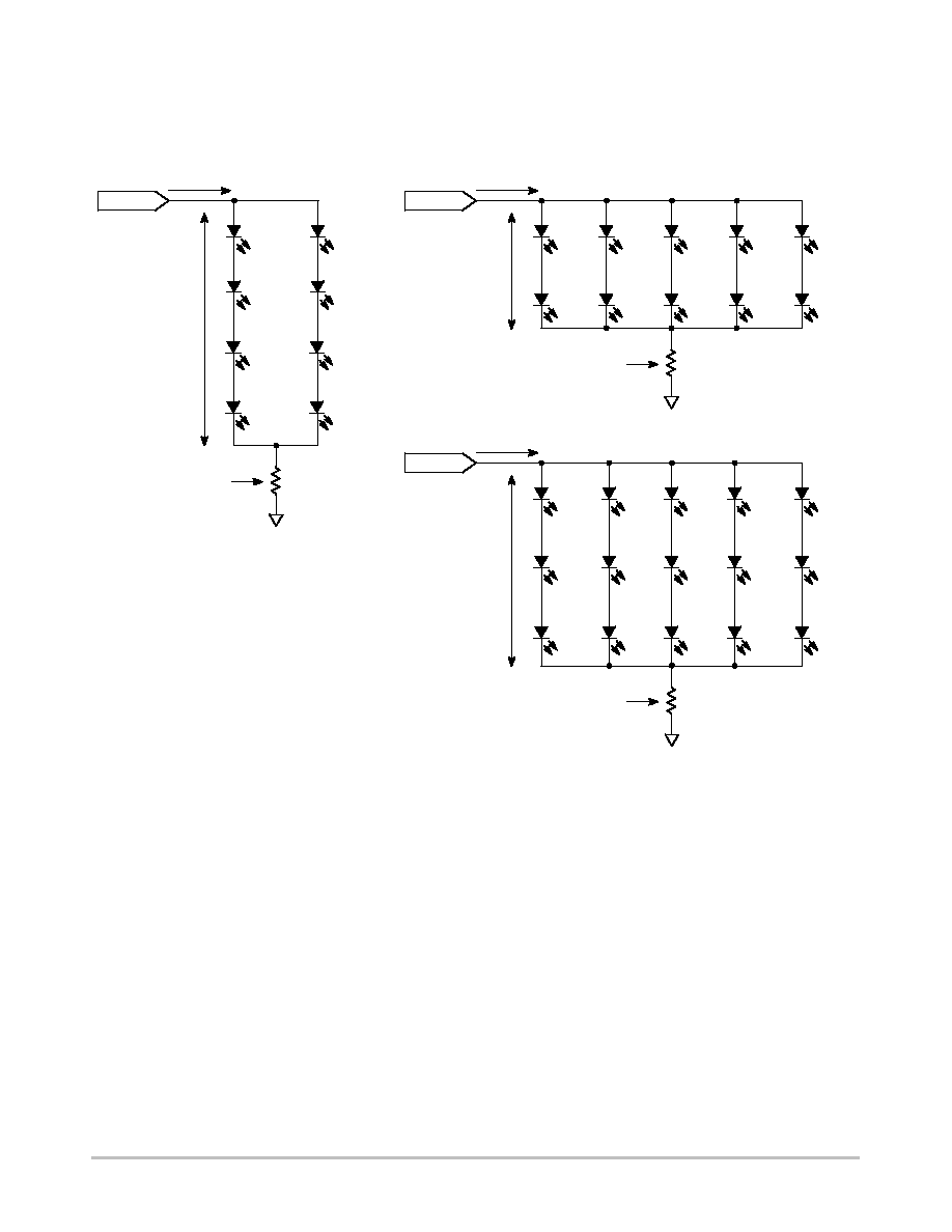
Typical LEDs Load Mapping
Since the output power is battery limited (see Figure 5),
one can arrange the LEDs in a variety of different
configurations. Powering ten LEDs can be achieved by a
series/parallel combination as depicted in Figure 31.
Figure 31. Examples of Possible LED Arrangements
D1
LED
D2
LED
D3
LED
D4
LED
D5
LED
D6
LED
D7
LED
D8
LED
D9
LED
D10
LED
Load
75 mA
7.0 V (T
yp.)
D1
LED
D2
LED
D3
LED
D4
LED
Load
50 mA
14 V (T
yp.)
D1
LED
D2
LED
Load
60 mA
10.5 V (T
yp.)
D3
LED
D4
LED
D5
LED
D6
LED
D7
LED
D8
LED
D9
LED
D5
LED
D6
LED
D7
LED
D8
LED
D10
LED
D11
LED
D12
LED
D13
LED
D14
LED
D15
LED
GND
R1
3.9
W
Sense
Resistor
Test conditions: V
bat
= 3.6 V
L
out
= 22
m
H
C
out
= 1.0
m
F
GND
R1
2.7
W
Sense
Resistor
GND
R1
3.3
W
Sense
Resistor
NCP5007
http://onsemi.com
18
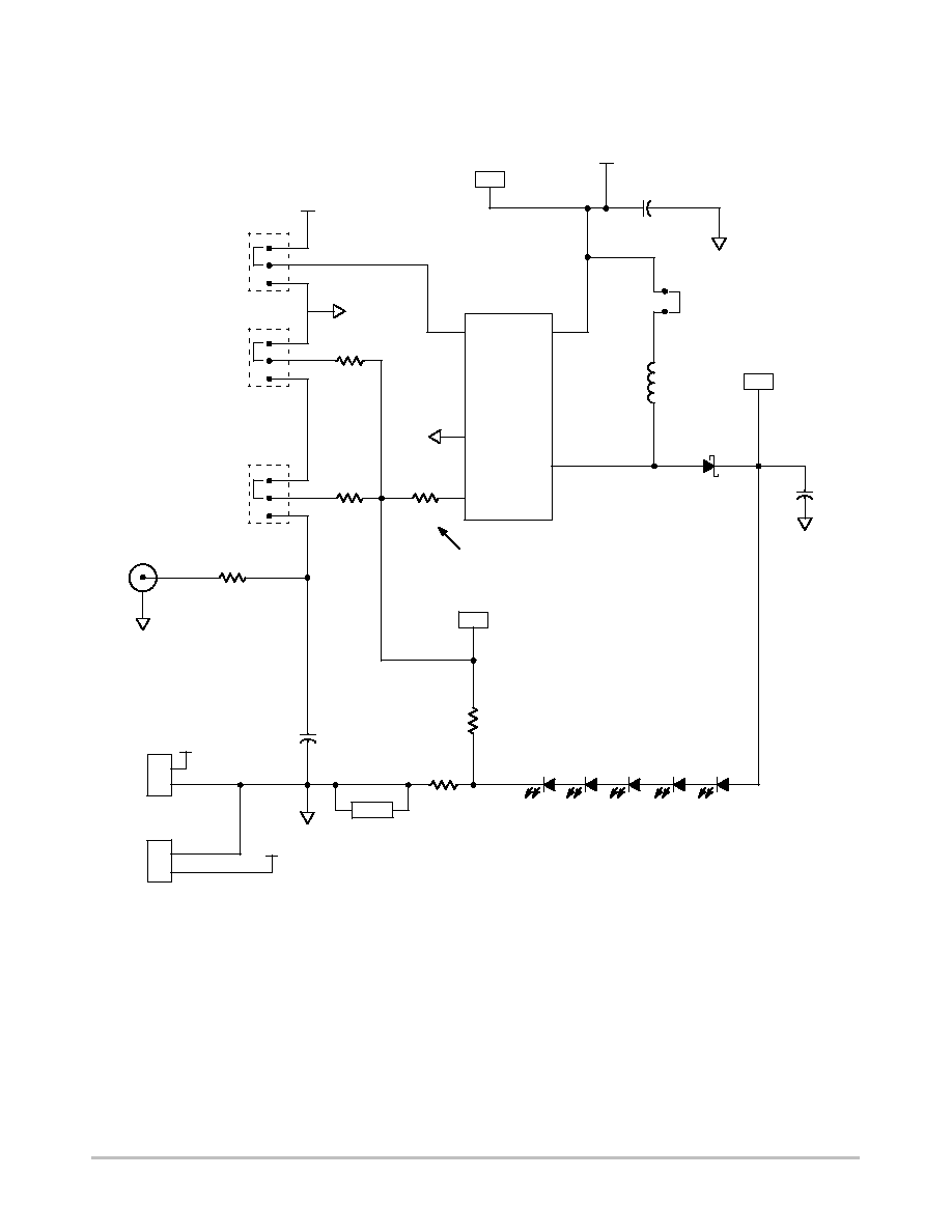
ON Semiconductor provides a demo board to evaluate the performance of the NCP5007. The schematic for that demo board
is illustrated in Figure 32.
Figure 32. NCP5007 Demo Board Schematic Diagram
EN
5
V
out
V
bat
NCP5007
L1
22
m
H
V
bat
C1
4.7
m
F/10 V
D6
D5
D4
D3
U1
3
D2
2
GND
GND
FB
1
D1
MBR0530
LED
LED
LED
LED
LED
R2
10 k
GND
JP1
ISense
4
TP1
V
out
C3
GND
TP3
V
bat
2
1
3
S2
SELECT
2
1
3
S1
MANUAL
2
1
3
S3
BRIGHTNESS
R5
0 R
GND
R3
10 k
Jumper = 0
W
MODULATION
R1
150 k
GND
J3
TP2
FB
R4
5.6 k
GND
C2
100 nF
2
1
V
bat
J2
PWR
1
2
J1
V
bat
GND
Z1
R10
10 R
V
bat
NCP5007
http://onsemi.com
19
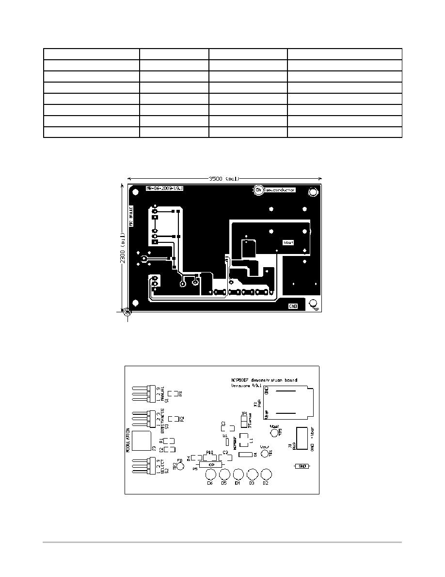
Table 1. Recommended External Parts
Part
Manufacturer
Description
Part Number
30 V Low Vf Schottky Diode
ON Semiconductor
SOD-123 (1.6 x 3.2 mm)
MBR0530T1
20 V Low Vf Schottky Diode
ON Semiconductor
SOD-323 (1.25 x 2.5 mm)
NSR0320MW2T1
20 V Low Vf Schottky Diode
ON Semiconductor
SOD-563 (1.6 x 1.6 mm)
NSR0320XV6T1
Ceramic Cap. 1.0
m
F/16 V
MURATA
GRM42-X7R
GRM42-6X7R-105K16
Ceramic Cap. 4.7
m
F/6.3 V
MURATA
GRM40-X5R
GRM40-X5R-475K6.3
Inductor 22
m
H
CoilCraft
1008PS-Shielded
1008PS-223MC
Inductor 22
m
H
CoilCraft
Power Wafer
LPQ4812-223KXC
Figure 33. NCP5007 Demo Board PCB: Top Layer
Figure 34. NCP5007 Demo Board Top Silkscreen

NCP5007
http://onsemi.com
20
FIGURES INDEX
Figure 1:
Typical Application
1
. . . . . . . . . . . . . . . . . . . . . . . . . . . . . . . . . . . . . . . . . . . . . . . . . . . . . . . . . . . . . . . . . . . . . .
Figure 2:
Block Diagram
2
. . . . . . . . . . . . . . . . . . . . . . . . . . . . . . . . . . . . . . . . . . . . . . . . . . . . . . . . . . . . . . . . . . . . . . . . . .
Figure 3:
Basic DC-DC Converter Structure
5
. . . . . . . . . . . . . . . . . . . . . . . . . . . . . . . . . . . . . . . . . . . . . . . . . . . . . . . . . . .
Figure 4:
Basic DC-DC Operation
6
. . . . . . . . . . . . . . . . . . . . . . . . . . . . . . . . . . . . . . . . . . . . . . . . . . . . . . . . . . . . . . . . . .
Figure 5:
Maximum Output Power as a Function of the Battery Supply Voltage
7
. . . . . . . . . . . . . . . . . . . . . . . . . . . . . . .
Figure 6:
Typical Inductor Peak Current as a Function of V
bat
Voltage
7
. . . . . . . . . . . . . . . . . . . . . . . . . . . . . . . . . . . . . .
Figure 7:
Maximum Output Current as a Function of V
bat
7
. . . . . . . . . . . . . . . . . . . . . . . . . . . . . . . . . . . . . . . . . . . . . . . .
Figure 8:
Output Current Feedback
8
. . . . . . . . . . . . . . . . . . . . . . . . . . . . . . . . . . . . . . . . . . . . . . . . . . . . . . . . . . . . . . . . . .
Figure 9:
Basic Schematic Diagram
8
. . . . . . . . . . . . . . . . . . . . . . . . . . . . . . . . . . . . . . . . . . . . . . . . . . . . . . . . . . . . . . . . . .
Figure 10: Overall Efficiency vs. Power Supply - I
out
= 4.0 mA, L = 22
mH
9
. . . . . . . . . . . . . . . . . . . . . . . . . . . . . . . . . . .
Figure 11: Overall Efficiency vs. Power Supply - I
out
= 10 mA, L = 22
mH
9
. . . . . . . . . . . . . . . . . . . . . . . . . . . . . . . . . . .
Figure 12: Overall Efficiency vs. Power Supply - I
out
= 15 mA, L = 22
mH
9
. . . . . . . . . . . . . . . . . . . . . . . . . . . . . . . . . . .
Figure 13: Overall Efficiency vs. Power Supply - I
out
= 20 mA, L = 22
mH
9
. . . . . . . . . . . . . . . . . . . . . . . . . . . . . . . . . . .
Figure 14: Overall Efficiency vs. Power Supply - I
out
= 40 mA, L = 22
mH
10
. . . . . . . . . . . . . . . . . . . . . . . . . . . . . . . . . .
Figure 15: Feedback Voltage Stability
10
. . . . . . . . . . . . . . . . . . . . . . . . . . . . . . . . . . . . . . . . . . . . . . . . . . . . . . . . . . . . . . . .
Figure 16: Feedback Voltage Variation
10
. . . . . . . . . . . . . . . . . . . . . . . . . . . . . . . . . . . . . . . . . . . . . . . . . . . . . . . . . . . . . . .
Figure 17: Standby Current
10
. . . . . . . . . . . . . . . . . . . . . . . . . . . . . . . . . . . . . . . . . . . . . . . . . . . . . . . . . . . . . . . . . . . . . . . .
Figure 18: Typical Operating Frequency
10
. . . . . . . . . . . . . . . . . . . . . . . . . . . . . . . . . . . . . . . . . . . . . . . . . . . . . . . . . . . . . .
Figure 19: Overvoltage Protection
10
. . . . . . . . . . . . . . . . . . . . . . . . . . . . . . . . . . . . . . . . . . . . . . . . . . . . . . . . . . . . . . . . . . .
Figure 23: Typical Power Up Response
12
. . . . . . . . . . . . . . . . . . . . . . . . . . . . . . . . . . . . . . . . . . . . . . . . . . . . . . . . . . . . . . .
Figure 24: Typical Startup Inductor Current and Output Voltage
12
. . . . . . . . . . . . . . . . . . . . . . . . . . . . . . . . . . . . . . . . . . .
Figure 25: Typical Inductor Current
13
. . . . . . . . . . . . . . . . . . . . . . . . . . . . . . . . . . . . . . . . . . . . . . . . . . . . . . . . . . . . . . . . . .
Figure 26: Typical Output Voltage Ripple
13
. . . . . . . . . . . . . . . . . . . . . . . . . . . . . . . . . . . . . . . . . . . . . . . . . . . . . . . . . . . . .
Figure 27: Typical Output Peak Voltage
14
. . . . . . . . . . . . . . . . . . . . . . . . . . . . . . . . . . . . . . . . . . . . . . . . . . . . . . . . . . . . . .
Figure 28: Basic DC Current Mode Operation with Analog Feedback
15
. . . . . . . . . . . . . . . . . . . . . . . . . . . . . . . . . . . . . . .
Figure 29: Basic DC Current Mode Operation with PWM Control
16
. . . . . . . . . . . . . . . . . . . . . . . . . . . . . . . . . . . . . . . . .
Figure 30: Typical Semi-Pulsed Mode of Operation
16
. . . . . . . . . . . . . . . . . . . . . . . . . . . . . . . . . . . . . . . . . . . . . . . . . . . . .
Figure 31: Examples of Possible LED Arrangements
17
. . . . . . . . . . . . . . . . . . . . . . . . . . . . . . . . . . . . . . . . . . . . . . . . . . . .
Figure 32: NCP5007 Demo Board Schematic Diagram
18
. . . . . . . . . . . . . . . . . . . . . . . . . . . . . . . . . . . . . . . . . . . . . . . . . .
Figure 33: NCP5007 Demo Board PCB: Top Layer
19
. . . . . . . . . . . . . . . . . . . . . . . . . . . . . . . . . . . . . . . . . . . . . . . . . . . . .
Figure 34: NCP5007 Demo Board Top Silkscreen
19
. . . . . . . . . . . . . . . . . . . . . . . . . . . . . . . . . . . . . . . . . . . . . . . . . . . . . .
NOTE CAPTIONS INDEX
Note 1:
This device series contains ESD protection and exceeds the following tests
4
. . . . . . . . . . . . . . . . . . . . . . . . . . .
Note 2:
The maximum package power dissipation limit must not be exceeded
4
. . . . . . . . . . . . . . . . . . . . . . . . . . . . . . .
Note 3:
Latchup current maximum rating:
"100 mA per JEDEC standard: JESD78
4
. . . . . . . . . . . . . . . . . . . . . . . . . .
Note 4:
Moisture Sensivity Level (MSL): 1 per IPC/JEDEC standard: J-STD-020A
4
. . . . . . . . . . . . . . . . . . . . . . . . . .
Note 5:
The overall tolerance depends upon the accuracy of the external resistor
5
. . . . . . . . . . . . . . . . . . . . . . . . . . . . .
ABBREVIATIONS
EN
Enable
FB
Feed Back
POR
Power On Reset: Internal pulse to reset the chip when the power supply is applied
NCP5007
http://onsemi.com
21
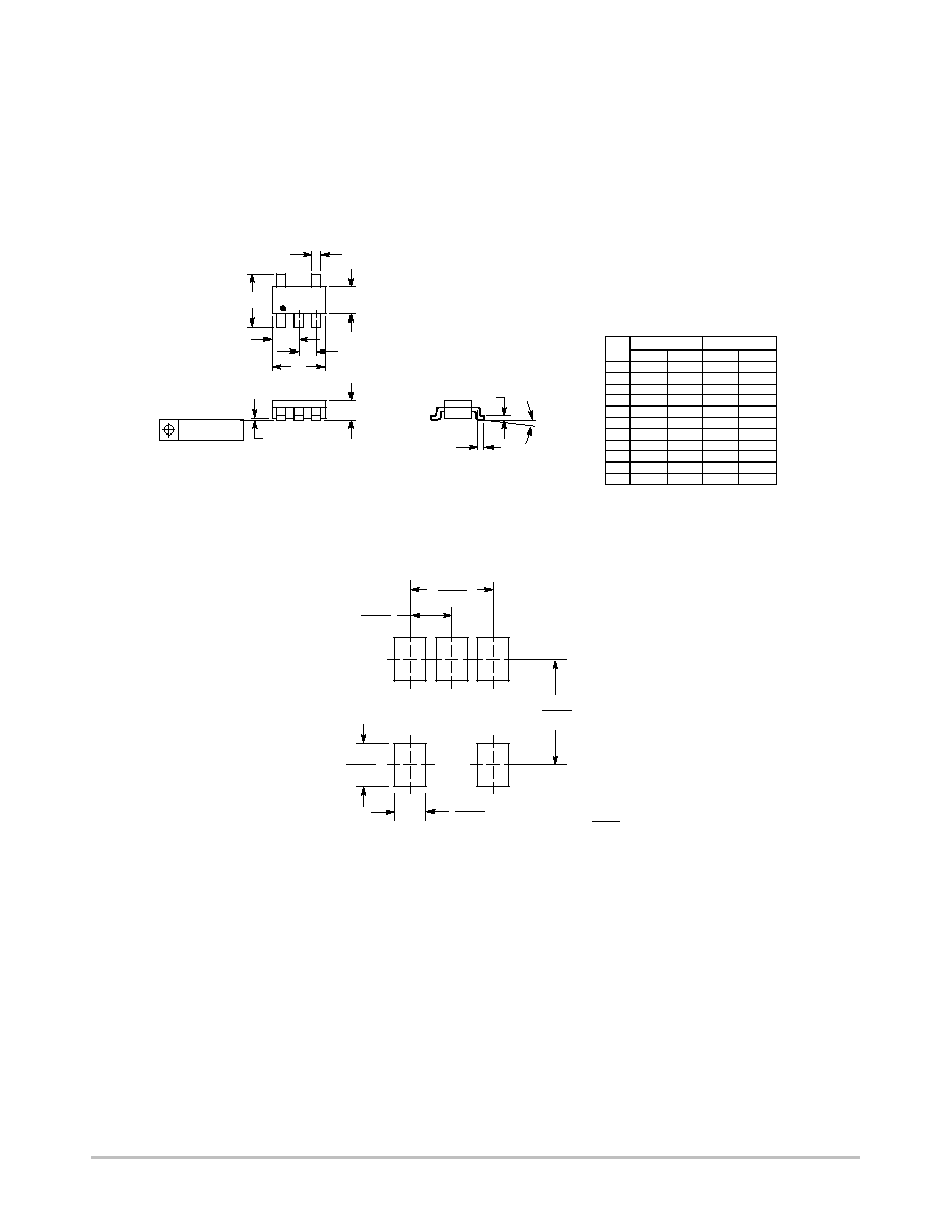
PACKAGE DIMENSIONS
TSOP-5
SN SUFFIX
CASE 483-02
ISSUE C
NOTES:
1. DIMENSIONING AND TOLERANCING PER
ANSI Y14.5M, 1982.
2. CONTROLLING DIMENSION: MILLIMETER.
3. MAXIMUM LEAD THICKNESS INCLUDES
LEAD FINISH THICKNESS. MINIMUM LEAD
THICKNESS IS THE MINIMUM THICKNESS
OF BASE MATERIAL.
4. A AND B DIMENSIONS DO NOT INCLUDE
MOLD FLASH, PROTRUSIONS, OR GATE
BURRS.
DIM
MIN
MAX
MIN
MAX
INCHES
MILLIMETERS
A
2.90
3.10 0.1142 0.1220
B
1.30
1.70 0.0512 0.0669
C
0.90
1.10 0.0354 0.0433
D
0.25
0.50 0.0098 0.0197
G
0.85
1.05 0.0335 0.0413
H
0.013
0.100 0.0005 0.0040
J
0.10
0.26 0.0040 0.0102
K
0.20
0.60 0.0079 0.0236
L
1.25
1.55 0.0493 0.0610
M
0
10
0
10
S
2.50
3.00 0.0985 0.1181
0.05 (0.002)
1
2
3
5
4
S
A
G
L
B
D
H
C
K
M
J
_
_
_
_
0.7
0.028
1.0
0.039
mm
inches
SCALE 10:1
0.95
0.037
2.4
0.094
1.9
0.074
*For additional information on our Pb-Free strategy and soldering
details, please download the ON Semiconductor Soldering and
Mounting Techniques Reference Manual, SOLDERRM/D.
SOLDERING FOOTPRINT*

NCP5007
http://onsemi.com
22
ON Semiconductor and are registered trademarks of Semiconductor Components Industries, LLC (SCILLC). SCILLC reserves the right to make changes without further notice
to any products herein. SCILLC makes no warranty, representation or guarantee regarding the suitability of its products for any particular purpose, nor does SCILLC assume any liability
arising out of the application or use of any product or circuit, and specifically disclaims any and all liability, including without limitation special, consequential or incidental damages.
"Typical" parameters which may be provided in SCILLC data sheets and/or specifications can and do vary in different applications and actual performance may vary over time. All
operating parameters, including "Typicals" must be validated for each customer application by customer's technical experts. SCILLC does not convey any license under its patent rights
nor the rights of others. SCILLC products are not designed, intended, or authorized for use as components in systems intended for surgical implant into the body, or other applications
intended to support or sustain life, or for any other application in which the failure of the SCILLC product could create a situation where personal injury or death may occur. Should
Buyer purchase or use SCILLC products for any such unintended or unauthorized application, Buyer shall indemnify and hold SCILLC and its officers, employees, subsidiaries, affiliates,
and distributors harmless against all claims, costs, damages, and expenses, and reasonable attorney fees arising out of, directly or indirectly, any claim of personal injury or death
associated with such unintended or unauthorized use, even if such claim alleges that SCILLC was negligent regarding the design or manufacture of the part. SCILLC is an Equal
Opportunity/Affirmative Action Employer. This literature is subject to all applicable copyright laws and is not for resale in any manner.
PUBLICATION ORDERING INFORMATION
N. American Technical Support: 800-282-9855 Toll Free
USA/Canada
Japan: ON Semiconductor, Japan Customer Focus Center
2-9-1 Kamimeguro, Meguro-ku, Tokyo, Japan 153-0051
Phone: 81-3-5773-3850
NCP5007/D
LITERATURE FULFILLMENT:
Literature Distribution Center for ON Semiconductor
P.O. Box 61312, Phoenix, Arizona 85082-1312 USA
Phone: 480-829-7710 or 800-344-3860 Toll Free USA/Canada
Fax: 480-829-7709 or 800-344-3867 Toll Free USA/Canada
Email: orderlit@onsemi.com
ON Semiconductor Website: http://onsemi.com
Order Literature: http://www.onsemi.com/litorder
For additional information, please contact your
local Sales Representative.