Äîêóìåíòàöèÿ è îïèñàíèÿ www.docs.chipfind.ru
©
Semiconductor Components Industries, LLC, 2003
August, 2003 - Rev. 4
1
Publication Order Number:
NCP5008/D
NCP5008, NCP5009
Backlight LED Boost Driver
The NCP5008/NCP5009 is a high efficiency boost converter
operating in current loop control mode to drive Light Emitting
Diode. The current mode regulation allows a uniform brightness of
the LEDs.
Features
·
2.7 to 6.0 V Input Voltage Range
·
Output Voltage from V
bat
to 15 V
·
3.0
mA Quiescent Supply Current
·
Automatically LEDs Current Matching
·
No External Sense Resistor
·
Includes Dimming Function
·
Programmable or Automatic Current Output Mode
·
LOCAL or REMOTE Control Facility
·
Photo Transistor Sense Feedback Input
·
Inductor Based Converter brings High Efficiency
·
Low Noise DC/DC Converter
·
All Pins are Fully ESD Protected
Typical Applications
·
LED Display Back Light Control
·
High Efficiency Step Up Converter
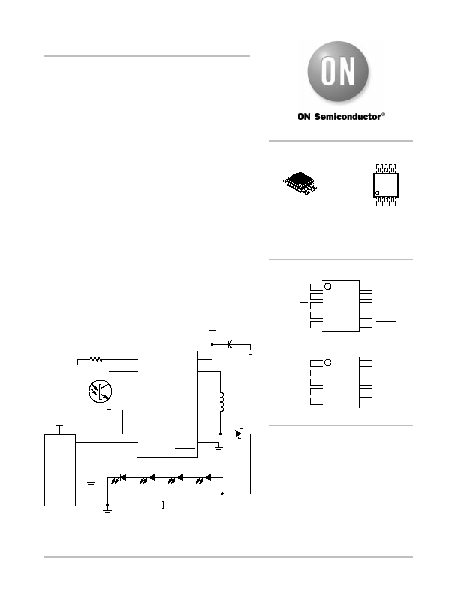
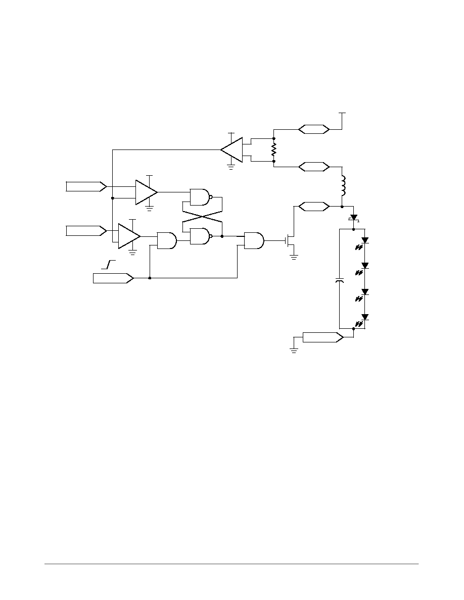
Figure 1. Typical Battery Powered LED Boost Driver
I
ref
PHOTO
L2
CS
CLK
1
2
Q1
NPN-PHOTO
GND
4
V
bat
3
5
6
LOCAL
GND
7
4
8
GND
L1
9
V
bat
10
R1
30 k
GND
MICROCONTROLLER
Vcc
GND
NCP5009
L1
22
m
H
V
bat
C1
10
m
F/6.3 V
GND
D5 MBR0520
LED
D1
LED
D2
LED
D3
LED
D4
2.2
m
F/16 V
C2
GND
U1
VBIAS
Micro 10
DM SUFFIX
CASE 846B
PIN CONNECTIONS
I
ref
V
bat
NC
CS
VBIAS
L1
L2 Iout
GND
1
10
2
3
4
9
8
7
10
1
5Tx
AYW
MARKING
DIAGRAM
x
= Device Number 8 or 9
A
= Assembly Location
Y
= Year
W
= Work Week
CLOCK
5
LOCAL
6
I
ref
V
bat
Photo
CS
VBIAS
L1
L2 Iout
GND
1
10
2
3
4
9
8
7
CLOCK
5
LOCAL
6
NCP5008
NCP5009
See detailed ordering and shipping information in the package
dimensions section on page 18 of this data sheet.
ORDERING INFORMATION
http://onsemi.com
NCP5008, NCP5009
http://onsemi.com
2
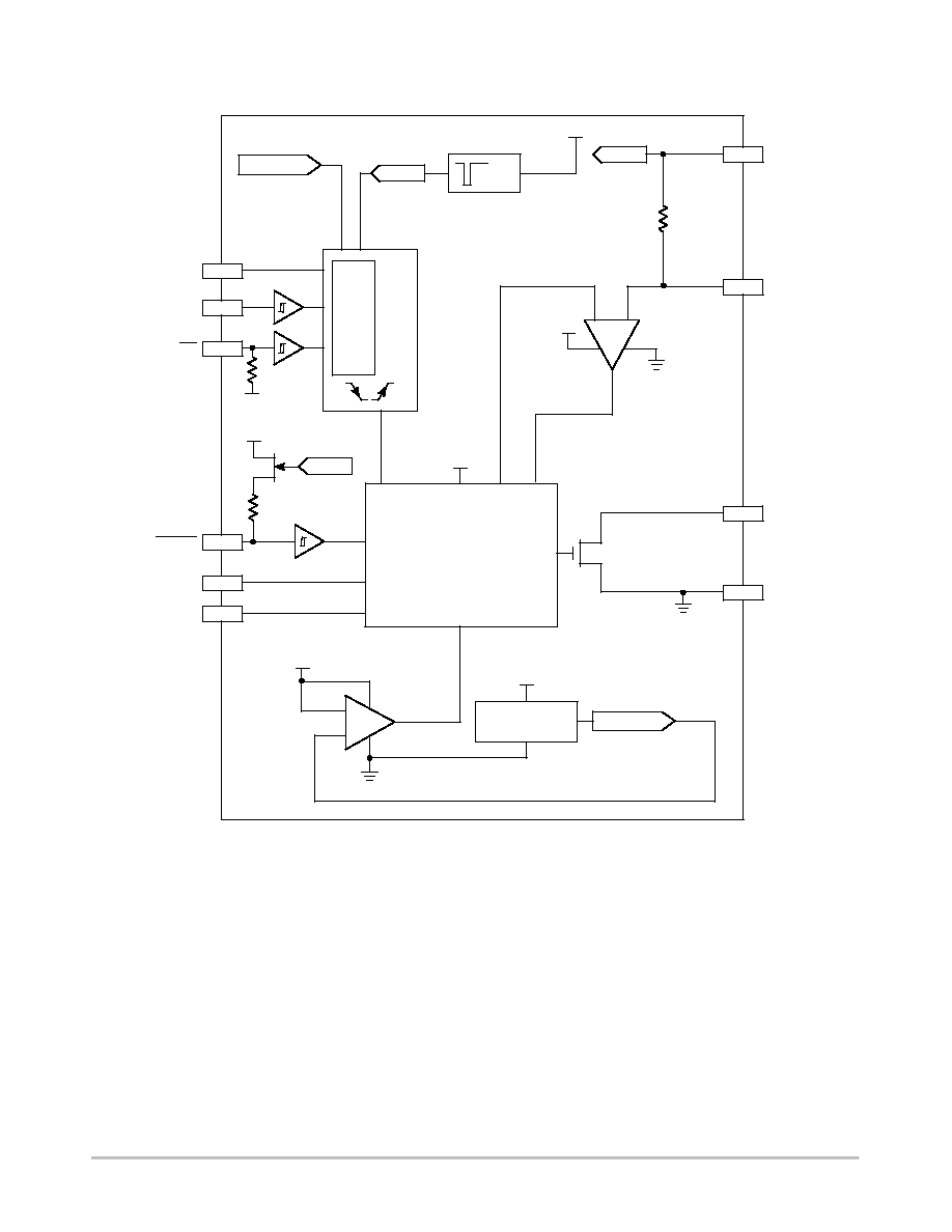
Figure 2. Block Diagram
BACK LIGHT WHITE LED CURRENT DRIVE CONTROLLER
BandGap
POR
POR
V
bat
V
bat
10
R1
1R8
V
bat
Isense
9
L1
A=10
+
-
Iout Reference
GND
V
bat
CONTROLLER
8
L2
7
GND
Iout
Q1
GND
BANDGAP
REFERENCE
V
bat
BandGap
V
bat
_OK
2
PHOTO
(See Note)
1
I
ref
6
LOCAL
V
bat
POR
50 k
Q2
Serial T
o
Parallel
Latches
1:8
V
ref
Selection
V
ref
4
VBIAS
5
CLK
3
CS
NOTE: This functionality is NOT implemented on the NCP5008 type.
50 k
V
bat
GND
V
bat
V
bat
+
-
NCP5008, NCP5009
http://onsemi.com
3
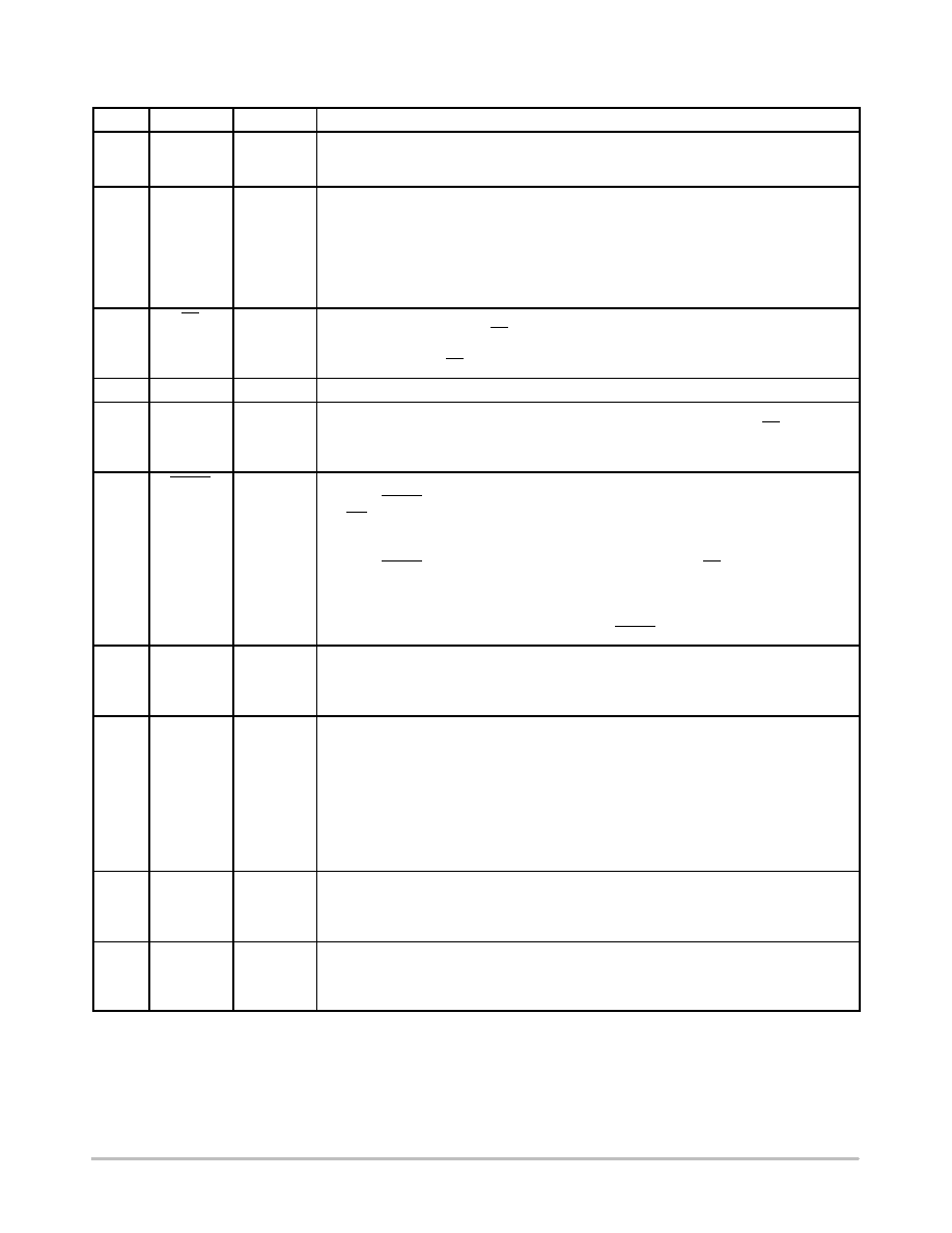
PIN FUNCTION DESCRIPTION
Pin
Symbol
Type
Description
1
I
ref
INPUT
This pin provides the output current range adjustment by means of a resistor connected to
ground. The current output tolerance depends upon the accuracy of this resistor. Using a
"
1%
metal film resistor, or better, yields the best output current accuracy.
2
PHOTO
SIGNAL
This pin provides an access to the output current control loop for the NCP5009 version. The
current sunk to ground from this pin is subtracted from the output current mirror. Primary use is
the ambient light automatic adjustment by means of an external photo transistor connected
across this pin and ground. The output current decreases as the ambient light increases. The
internal circuit provides a 1/1 current ratio with the I
ref
defined by the resistor connected from pin
1 to ground. This current shall be limited to 65
m
A.
This functionality is NOT implemented on the NCP5008 type.
3
CS
INPUT
Negative going Chip Select logic input. This pin is used to select the NCP5008/ NCP5009 and
validate the clock/data when CS = Low. The internal shift register is automatically clear to zero
upon the falling edge, thanks to a 20 ns built-in one shoot. The built-in pull-up resistor disables
the device when the CS pin is left open.
4
VBIAS
POWER
This pin should be connected to V
bat
.
5
CLOCK
INPUT
The clock signal connected to this pin is used to serially shift right the internal preset high logic
level. The clock is valid between the falling edge and until the rising edge of the CS. There is
neither a feedback nor an overflow control. If the clock count exceeds 8 bits, the internal register
is clear, the output current is forced to zero and the device comes back to the shutdown mode.
6
LOCAL
INPUT
This pin is used to select the mode of operation.
·
When LOCAL = High or Open, the chip is controlled by two digital lines:
CS and CLOCK. The output current is programmed by the logic control
of these pins, allowing a current adjustment within the range defined by the
I
ref
resistor.
·
When LOCAL = Low, the chip is turned ON /OFF by means of the CS line,
the CLOCK pins being deactivated. The output current is constant, as defined
by the I
ref
resistor value.
In order to minimize the standby current a dynamic pull-up resistor is activated when POR is
High, this pull-up resistor being disconnected when LOCAL = Low.
7
GND
POWER
This pin is the system ground for the NCP5008/NCP5009 and carries both the Power and the
Digital signals. High quality ground must be provided to avoid spikes and/or uncontrolled
operation. Care must be observed to avoid high-density current flow in a limited PCB copper
track.
8
L2
POWER
This pin is the power side of the external inductor and must be connected either to the external
Schottky diode (see Figure 22) or directly to one external LED (see Figure 23). It provides the
output current to the load. Since the boost converter operates in a current loop mode, the output
voltage can range up to +15 V but shall not extend this limit. The user must make sure this
voltage will not be exceeded during the normal operation of this part.
An external low cost ceramic capacitor (2.2
m
F/16 V, ESR < 100 m
W
) is recommended to
smooth the current flowing into the diode(s), thus limiting the noise created by the fast transients
present in this circuitry.
Care must be observed to avoid EMI though the PCB copper tracks connected to this pin.
9
L1
POWER
The return side of the external inductor shall be connected to this pin. Typical application will
use a 22
m
H, size 1210, to handle the 2.8 to 364 mA max range. On the other hand, when the
desired output current is above 20 mA, the inductor shall have an ESR < 1.0
W
. The output
current tolerance can be improved by using a larger inductor value.
10
V
bat
POWER
The external voltage supply is connected to this pin. A high quality reservoir capacitor must be
connected across pin 10 and Ground to achieve the specified output voltage parameters. A
10
m
F/6.3 V, low ESR capacitor must be connected as close as possible across pin 10 and
ground pin 7. The X5R ceramic types are recommended.
NCP5008, NCP5009
http://onsemi.com
4
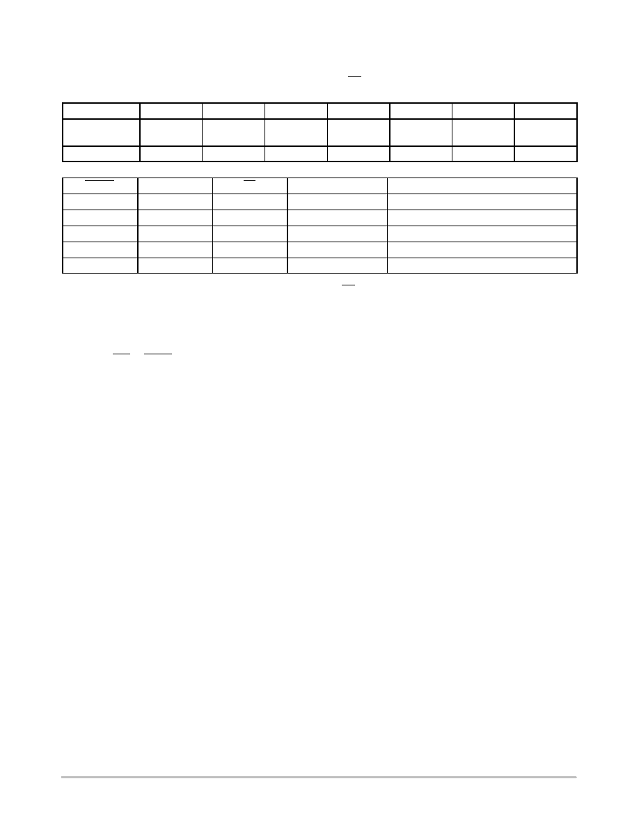
Table 1. Shift Register Bits Assignment and Functions
SetReg shift register
(Note:
The register content is latched upon CS positive going).
B7
B6
B5
B4
B3
B2
B1
Bn Value
After POR
0
0
0
0
0
0
0
Iout Peak (mA)
I
ref
*k*7.5
I
ref
*k*6.5
I
ref
*k*5.5
I
ref
*k*4.5
I
ref
*k*3.5
I
ref
*k*2.5
I
ref
*k*1.5
LOCAL
CLOCK
CS
B1-B7
Output Current
L
X
H
X
0
L
X
L
X
I
ref
* k
H or Open
X
H
No Change
I
ref
* k * (Bn + 0.5)
H or Open
L
No Change
I
ref
* k * (Bn + 0.5)
H or Open
L
Q
data
Bn
I
ref
* k * (Bn + 0.5)
The register is clear to zero during the first 20 ns following the CS falling edge.
Note:
Coefficient Value (internal ratio): k = 746
Maximum output peak current @ B7 = 1 and Iphoto = 0
mA :Iout peak = I
ref
* (7 + 0.5) * 746 = I
ref
* 5595
Iref
+
Vref
R1
+
1.24 V
R1
NCP5008, NCP5009
http://onsemi.com
5
MAXIMUM RATINGS
Rating
Symbol
Value
Unit
Power Supply
V
bat
, V
BIAS
7.0
V
Output Power Supply Voltage Compliance
V
L2
16
V
Digital Input Voltage
Digital Input Current
CLK, CS
-0.3
t
V
t
V
bat
+ 3.0 V
1.0
V
mA
Human Body Model: R = 1500
W
, C = 100 pF
ESD
"
2.0
kV
Machine Model
ESD
"
200
V
Micro 10 Package
Power Dissipation @ T
A
= +85
°
C
Thermal Resistance Junction-to-Air
P
D
R
Thja
200
200
mW
°
C/W
Operating Ambient Temperature Range
T
A
-25 to +85
°
C
Operating Junction Temperature Range
T
J
-25 to +125
°
C
Maximum Junction Temperature
T
Jmax
+150
°
C
Storage Temperature Range
T
stg
-65 to +150
°
C
Maximum Ratings are those values beyond which damage to the device may occur. Exposure to these conditions or conditions beyond those
indicated may adversely affect device reliability. Functional operation under absolute maximum-rated conditions is not implied. Functional
operation should be restricted to the Recommended Operating Conditions.
POWER SUPPLY SECTION
(-25
°
C to +85
°
C ambient temperature, unless otherwise noted.)
Rating
Pin
Symbol
Min
Typ
Max
Unit
Power Supply
10
V
bat
2.7
-
6.0
V
Power Supply Threshold Start Up Voltage
10
V
batThr
-
2.3
2.7
V
Output Load Voltage Compliance
8
V
out
-
-
15.0
V
Pulsed Current Regulation Range
8
I
out
0
-
400
mA
Continuous DC Current in the Load
8
I
out
-
-
75
mA
Output Pulsed Current Tolerance @ V
bat
= 3.6 V, L1 = 22
m
H/0.71
W
,
R
ref
"
1%, I
LED
= 20 mA (Note 1)
8
I
out
-
"
5.0
-
%
Output Leakage @ LOCAL = 0, CS = H, Vout = 15 V, V
bat
= 6.0 V
8
I
out
-
-
500
nA
Standby Current @ Iout = 0 mA, CS = H, CLK = H, V
bat
= V
BIAS
= 3.6 V
10
I
stdb
-
3.0
-
m
A
Standby Current @ Iout = 0 mA, CS = H, CLK = H, V
bat
= V
BIAS
= 6.0 V
10
I
stdb
-
-
10
m
A
Operating Current @ V
bat
= V
BIAS
= 3.6 V, I
ref
= 30
m
A, CLK = H, CS = L,
LOCAL = Open
10
I
ope
-
600
-
m
A
Boost Internal Oscillator Clock @ L1 = 22
m
H, V
bat
= V
BIAS
= 3.6 V,
Iout = 20 mA (Vout = 14 V)
-
F
osc
-
300
-
kHz
1. The tolerance refers to the 20 mA to 70 mA current range.
NCP5008, NCP5009
http://onsemi.com
6
DIGITAL SECTION
(-25
°
C to +85
°
C ambient temperature, unless otherwise noted.)
Rating
Pin
Symbol
Min
Typ
Max
Unit
High Level Input Voltage
Low Level Input Voltage
Input Capacitance
3, 5
V
IH
V
IL
C
in
0.7 * V
bat
-
-
-
-
10
V
bat
0.3 * V
bat
-
V
V
pF
High Level Input Voltage
Low Level Input Voltage
Input Capacitance
6
V
IH
V
IL
C
in
-
-
-
0.6 * V
bat
0.4 * V
bat
10
-
-
-
V
V
pF
LOCAL Pull-up Resistor
6
R
loc
20
-
80
k
W
LOCAL Leakage Current
9
I
Loc
-
-
100
nA
CS Pull-up Resistor
3
R
cs
20
-
80
k
W
Minimum CS Low Time
3
Tcs
setup
250
-
-
ns
Clock Frequency
5
F
CLK
-
-
5.0
MHz
CLOCK tr and tf
5
tr
CLK
, tf
CLK
10
-
-
ns
Internal Register Clear
-
t
clear
10
30
-
ns
Internal Power on Reset Width
-
t
POR
-
100
-
m
s
2. Digital inputs undershoot < - 0.30 V, Digital inputs overshoot < 0.30 V.
ANALOG SECTION
(-25
°
C to +85
°
C ambient temperature, unless otherwise noted.)
Rating
Pin
Symbol
Min
Typ
Max
Unit
Output Voltage Range Reference
@ 2.5
m
A < I
ref
< 65
m
A (Note 3)
1
V
ref
1.20
1.24
1.28
V
Maximum Output Current Range Ratio
8
I
out
-
5595
-
-
Minimum Output Current Range Ratio
8
I
out
-
1119
-
-
Output Current Sense Resistor
10, 9
R
s
-
1.8
5.0
W
Output Voltage Range Reference
@ 2.5
m
A < Ipho < 65
m
A
2
V
pho
1.20
1.24
1.28
V
Output Current Stabilization tdelay following a DC/DC start up
8
I
outdly
-
100
-
m
s
Internal NMOS Resistor @ V
bat
= 3.6 V
8
QR
DSON
-
2.2
3.0
W
Internal Comparator Delay Time
-
Td
comp
-
60
-
ns
3. The overall tolerance depends upon the accuracy of the external resistor. Using a 1%/low PPM metal film resistor is recommended to achieve
"
5% output current tolerance.
NCP5008, NCP5009
http://onsemi.com
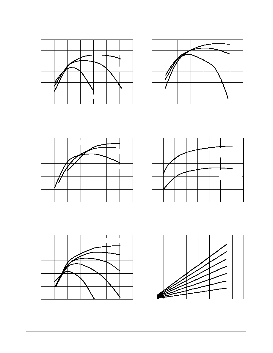
7
50
55
60
65
70
75
80
0
5
10
15
20
25
30
35
EFFICIENCY
(
%
)
Figure 3. Efficiency vs. Load Current @ 4 LEDS
(V
load
= 4*Vf
14.2 V)
Figure 4. Efficiency vs. Load Current @ 3 LEDS
(V
load
= 3*Vf
10.5 V)
Figure 5. Efficiency vs. Load Current @ 2 LEDS
(V
load
= 2*Vf
7.1 V)
60
65
70
75
80
85
0
5
10
15
20
25
30
35
Figure 6. Efficiency vs. V
bat
@
V
out
= 15 V/I
led
= 20mA and
V
out
= 7.5 V/I
led
= 40 mA
Figure 7. Efficiency vs. Load Current @ 4 LEDS
(V
load
= 2 strings of 2 LEDs in series = 7.1V)
Figure 8. Inductor peak Current vs.
I
ref
@ Bn = {1, 2, 3, 4, 5, 6, 7}
0
50
100
150
200
250
300
350
400
0
20
40
60
80
I
ref
(
m
A)
V
bat
= 3.6 V
V
bat
= 4.2 V
V
bat
= 3.0 V
I
LED
(mA)
50
55
60
65
70
75
80
0
5
10
15
20
25
30
35
EFFICIENCY
(
%
)
I
LED
(mA)
EFFICIENCY
(
%
)
I
LED
(mA)
100
2.5
3.0
3.5
4.0
4.5
5.0
5.5
6.0
EFFICIENCY
(
%
)
V
bat
(V)
6.5
V
out
=7.5 V
I
led
= 40 mA
V
out
= 15 V
I
led
= 20 mA
100
0
10
20
30
40
50
60
70
EFFICIENCY
(
%
)
I
LED
(mA)
I
peak
(mA)
V
bat
= 6.0 V
3.0 V
3.6 V
4.2 V
5.0 V
Bn
7
4
3
2
1
6
5
V
bat
= 3.6 V
V
bat
= 4.2 V
V
bat
= 3.0 V
V
bat
= 3.6 V
V
bat
= 4.2 V
V
bat
= 3.0 V
90
80
70
60
50
95
90
85
80
75
TYPICAL OPERATING CHARACTERISTICS
Condition: Typical Application: L = 22
m
H, Cin = 10
m
F, Cout = 2.2
m
F, R1 = 30 k
W
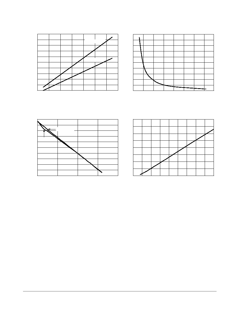
NCP5008, NCP5009
http://onsemi.com
8
Figure 9. Load Current (I
led
) vs. I
ref
@ V
bat
= 3.6 V, V
load
= 15 V and 10 V
0
5
10
15
20
25
30
35
40
45
50
0
10
20
30
40
50
60
70
I
ref
(
m
A)
Figure 10. Inductor Peak Current Error vs.
Theoretical Inductor Peak Current
0
2
4
6
8
10
12
14
16
18
20
0
50
100
150
200
250
300
350
400
Figure 11. Inductor Peak Current vs. I
photo
@ I
ref
= 34
m
A
0
20
40
60
80
100
120
140
160
180
200
0
10
20
30
40
Figure 12. Stand by Current vs. V
bat
@ T = 20
°
C
3.0
3.5
4.0
4.5
5.0
5.5
6.0
6.5
7.0
2.4
2.8
3.2
3.6
4.0
4.4
4.8
5.2
5.6
I
LED
(mA)
V
load
= 10 V
V
load
= 15 V
I
photo
(
m
A)
I
peak
(mA)
THEORETICAL I
peak
(mA)
I
peak
ERROR (%)
V
bat
(V)
6.0
TYPICAL OPERATING CHARACTERISTICS
Condition: Typical Application: L = 22
m
H, Cin = 10
m
F, Cout = 2.2
m
F, R1 = 30 k
W
Theoretical
Measured
I
stb
y
(
m
A)
NCP5008, NCP5009
http://onsemi.com
9
70
75
80
85
90
95
100
0
10
20
30
40
50
60
70
EFFICIENCY
(
%
)
V
bat
= 6.0 V
I
LED
(mA)
60
65
70
75
80
85
90
0
5
10
15
20
25
30
35
EFFICIENCY
(
%
)
I
LED
(mA)
50
55
60
65
70
75
80
0
5
10
15
20
25
30
35
EFFICIENCY
(
%
)
I
LED
(mA)
85
Figure 13. Efficiency vs. Load Current @ 4 LEDS
(V
load
= 4*Vf
14.2 V)
Figure 14. Efficiency vs. Load Current @ 3 LEDS
(V
load
= 3*Vf
10.5 V)
Figure 15. Efficiency vs Load Current @ 2 LEDS
(V
load
= 2*Vf
7.1 V)
Figure 16. Efficiency vs Load Current @ 4 LEDS
(V
load
= 2 strings of 2 LEDs in series = 7.1 V)
50
55
60
65
70
75
80
0
5
10
15
20
25
30
35
EFFICIENCY
(
%
)
V
bat
= 3.6 V
V
bat
= 4.2 V
V
bat
= 3.0 V
I
LED
(mA)
5.0 V
4.2 V
3.6 V
3.0 V
V
bat
= 3.6 V
V
bat
= 4.2 V
V
bat
= 3.0 V
V
bat
= 3.6 V
V
bat
= 4.2 V
V
bat
= 3.0 V
TYPICAL OPERATING CHARACTERISTICS
Condition: Typical Application: L = 22
m
H, Cin = 10
m
F, Cout = 2.2
m
F, R1 = 30 k
W
NCP5008, NCP5009
http://onsemi.com
10
Operating Description
Figure 17. Digital Timing Definitions
90%
50%
10%
t
CLKmin
tf
tr
Figure 18. Typical Schmitt Trigger Characteristic
V
bat
ON
OFF
Output
0.30* V
bat
0.70* V
bat
V
bat
Input
Input Schmitt Triggers
All the Logic Input pins have built-in Schmitt trigger
circuits to prevent the NCP5008/NCP5009 against
uncontrolled operation. The typical dynamic characteristics
of the related pins are depicted in Figure 18.
The output signal is guaranteed to go High when the
input voltage is above 0.70*V
bat
, and will go Low when the
input voltage is below 0.30*V
bat
.
Local Mode
When the system operate in a Local Mode (Pin 6,
/LOCAL=Low), the output current depends solely upon
the current drawn pin 1. The clock signal is irrelevant and
the output current is derived by equation I
out
= I
ref
* k, the
internal constant k being equal to 746.
ESD Protection
The NCP5008/NCP5009 includes silicon devices to
protect the pins against the ESD spikes voltages. To cope
with the different ESD voltages developed in the
applications, the built-in structures have been designed to
handle
$2.0 kV in Human Body Model (HBM) and
$200 V in Machine Model (MM) and on each pin.
NCP5008, NCP5009
http://onsemi.com
11
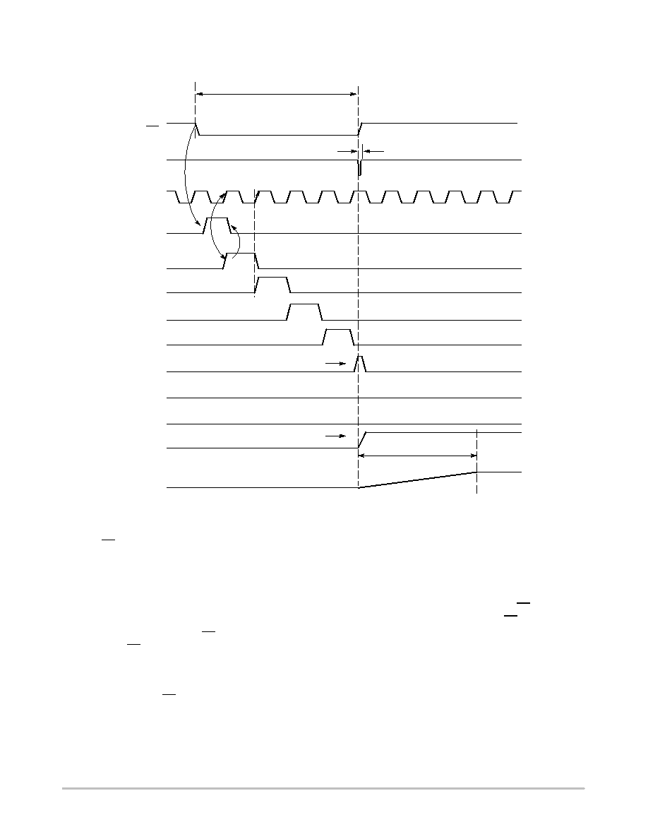
Remote Control Programming Sequence
Figure 19. Programming Sequence
I
out ref
Iout
B7
B6
B5
B4
B3
B2
B1
Qdata
CLK
CLEAR
CS
tCSsetup
tclear
Last Latched Bit
Output Current Programmed Register
Internal Latch Data and Reset
Ioutdly
Upon CS transition from High to Low, the internal
sequence will take place:
- Qdata is internally set to high level.
- Upon positive going transition of the next CLK signal,
the Qdata is shifted to the next Bn stage.
- Clear the Qdata flip-flop upon the positive going of
the SetReg[B1] transient.
The sequence keeps going until CS = High.
When the CS line returns to a High state, the
programming output current flip-flop is set according to
the previous state of the shift register and SetReg B[1-7] is
cleared afterward.
Depending upon the CS width, for a given CLK period,
the last SetReg bit will be latched and the output current
will be adjusted accordingly. If the number of CLK pulses
is higher than 7, the Qdata is lost and the SetReg register
bits B[1-7] are in the Low state, yielding a zero output
current.
The internal shift register can be clear by sending more
than 7 pulses to the CLK pin when the pin CS is low. If the
internal shift register is clear upon the CS transition from
Low to High, the device will be placed or maintained in the
shut down mode.
When the register content is higher than zero, the DC/DC
is activated and a 100
ms delay (typical) is necessary to
stabilize the output current to the programmed value.
NCP5008, NCP5009
http://onsemi.com
12
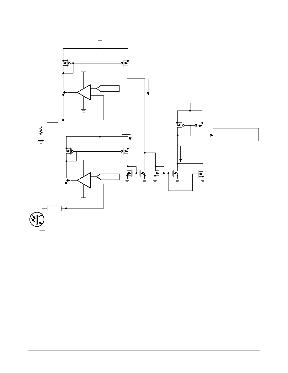
Set Up Output Current Range
Figure 20. Functional Diagram
V
bat
+
-
1
1
V
bat
BandGap
GND
I
ref
GND
V
bat
+
-
1
1
V
bat
BandGap
GND
Photo
Q1
NPN-PHOTO
GND
GND
GND
1:Bn
GND
GND
1
GND
2:1
V
bat
1
1:746
I = (I
ref
-Iphoto)*(Bn+0.5)
Iout Reference
= (I
ref
-Iphoto)*746*(Bn+0.5)
R
ref
30 k
I
ref
Iphoto
1
1
The current sunk to ground on PHOTO pin is subtracted
from the current sunk to ground on I
ref
pin. The result is
multiplied by the programmed value (Bn) and then
multiplied by the constant factor ratio (k = 746) in the
current mirror.
The constant factor k is a ratio between the current on
Iout sense and the Iout reference internally fixed.
The output current reference is:
Ipeak = Ivalley + (I
ref
- Iphoto) * Bn * k.
Where k = 746, Bn represents the bit of the internal shift
register, range from 1 to 7, and Ivalley = (I
ref
- Iphoto)
* 0.5 * k.
We can write also Ipeak = (I
ref
- Iphoto) * (Bn + 0.5) * k.
Please find below the formula to quickly calculate R1
resistor (resistor on I
ref
pin):
Iref
+
1.24
R1
NCP5008, NCP5009
http://onsemi.com
13
DC/DC Converter Operation
The DC/DC converter operates with a boost structure
depicted in Figure 21, the load being supplied by the pulsed
current coming from the external inductor L1. The current
is monitored by the internal sense resistor Rsense to Set and
Reset the flip-flop U3 and U6 according to the comparators
U2 and U4 output state.
Figure 21. Basic DC/DC Boost Structure
+
-
+
-
V
bat
GND
U1
Rsense
1R8
V
bat
L1
V
bat
L1
22
m
H
L2
Q1
GND
V
bat
GND
I
peak_ref
I
valley_ref
V
bat
+
-
U2
U4
GND
POR
U5
D4
LED
D3
LED
D2
LED
D1
LED
D5
MBR0520
GND
GND
C2
2.2
m
F/16 V
U7
U3
U6
NCP5008, NCP5009
http://onsemi.com
14
Output Load Drive
In order to make profit of the built-in Boost capabilities,
one shall operate the NCP5008/NCP5009 in the continuous
output current mode. Such a mode is achieved by using and
external reservoir capacitor (preferably a low ESR ceramic
type) across the LED as depicted in Figures 22, 23, 24, 25,
and 26.
Using an extra photo sensor is not mandatory and the
related pin 2 can be either left open or connected to V
bat
,
but must not be grounded on the NCP5009 version only.
At this point, the designer must carefully analyze two
parameters:
1. The output voltage must be limited to 15 V
maximum. It's the designer responsibility to
make sure that spike voltages beyond the
maximum rating will not exist across pin 8 and
ground. Depending upon a specific application
(V
bat
voltage, PCB layout
...
), using an external
voltage clamp could be necessary.
2. The peak current flowing into the LED diodes
shall be within the maximum ratings specified for
these devices.
The Schottky diode D5, associated with capacitor C2,
provides a rectification and filtering function.
When a pulse-operating mode is acceptable:
·
The LEDs brightness can be controlled in LOCAL
mode with a PWM on CS pin as depicted in Figure 24.
·
Or the Schottky can be removed and replaced by at
least one LED diode as depicted in Figure 23.
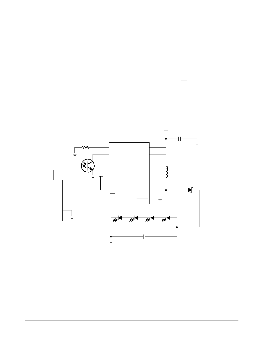
TYPICAL APPLICATION CIRCUIT
Figure 22. Basic DC Current Mode Operation in REMOTE Control
I
ref
PHOTO
L2
CS
CLK
1
2
Q1
NPN-PHOTO
GND
4
V
bat
3
5
6
LOCAL
GND
7
4
8
GND
L1
9
V
bat
10
R1
30 k
GND
MICROCONTROLLER
Vcc
GND
NCP5009
L1
22
m
H
V
bat
C1
10
m
F/6.3 V
GND
D5
MBR0520
LED
D1
LED
D2
LED
D3
LED
D4
2.2
m
F/16 V
C2
GND
U1
VBIAS
NCP5008, NCP5009
http://onsemi.com
15
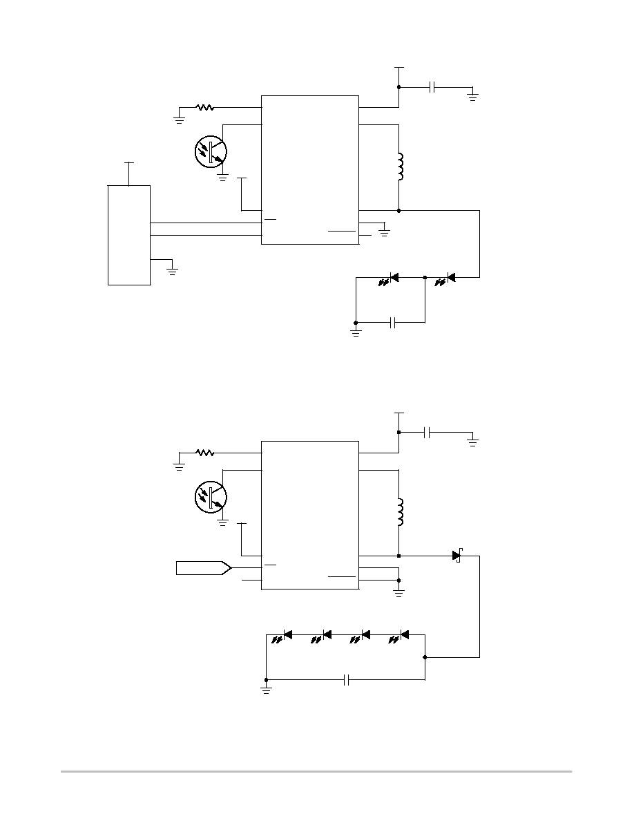
Figure 23. Typical Semi-Pulsed Mode of Operation in REMOTE Mode
I
ref
PHOTO
L2
CS
CLK
1
2
Q1
NPN-PHOTO
GND
4
V
bat
3
5
6
LOCAL
GND
7
4
8
GND
L1
9
V
bat
10
R1
30 k
GND
MICROCONTROLLER
Vcc
GND
NCP5009
L1
22
m
H
V
bat
C1
10
m
F/6.3 V
GND
LED
D3
LED
D4
1.0
m
F/16 V
C2
GND
U1
VBIAS
Figure 24. PWM Current Control Mode Operation in LOCAL Mode
I
ref
PHOTO
L2
CS
CLK
1
2
Q1
NPN-PHOTO
GND
4
V
bat
3
5
6
LOCAL
GND
7
4
8
L1
9
V
bat
10
R1
30 k
GND
NCP5009
L1
22
m
H
V
bat
C1
10
m
F/6.3 V
GND
D5
MBR0520
LED
D1
LED
D2
LED
D3
LED
D4
2.2
m
F/16 V
C2
GND
U1
VBIAS
PWM
GND
NCP5008, NCP5009
http://onsemi.com
16
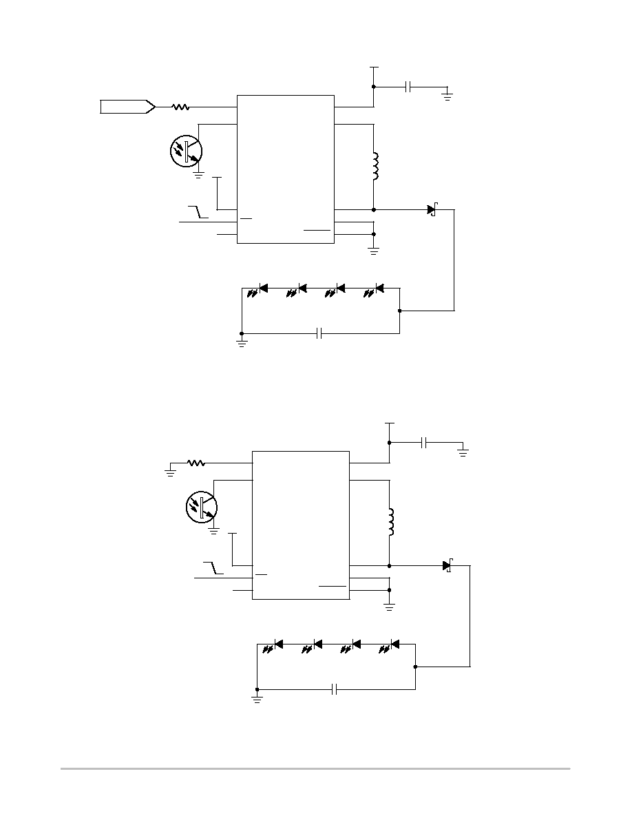
Figure 25. DAC Current Control Mode Operation in LOCAL Mode
I
ref
PHOTO
L2
CS
CLK
1
2
Q1
NPN-PHOTO
GND
4
V
bat
3
5
6
LOCAL
GND
7
4
8
L1
9
V
bat
10
R1
30 k
NCP5009
L1
22
m
H
V
bat
D5
MBR0520
LED
D1
LED
D2
LED
D3
LED
D4
2.2
m
F/16 V
C2
GND
U1
VBIAS
GND
DAC
OFF ON
C1
10
m
F/6.3 V
GND
Figure 26. Basic DC Current Mode Operation in LOCAL Mode
I
ref
PHOTO
L2
CS
CLK
1
2
Q1
NPN-PHOTO
GND
4
V
bat
3
5
6
LOCAL
GND
7
4
8
L1
9
V
bat
10
R1
30 k
NCP5009
L1
22
m
H
V
bat
D5
MBR0520
LED
D1
LED
D2
LED
D3
LED
D4
2.2
m
F/16 V
C2
GND
U1
VBIAS
GND
OFF ON
C1
10
m
F/6.3 V
GND
GND
NCP5008, NCP5009
http://onsemi.com
17
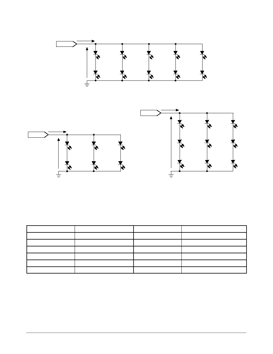
TYPICAL LEDS LOAD MAPPING
Figure 27. Three different examples of load can be driven by the NCP5009 or NCP5008
Condition: V
bat
= 3.6 V, L = 22
m
H
D1
LED
GND
D2
LED
D3
LED
D4
LED
D5
LED
D6
LED
D7
LED
D8
LED
D9
LED
D10
LED
Load+
75 mA
6.7 V
Example 1
D1
LED
D2
LED
D3
LED
D4
LED
D5
LED
D6
LED
Load+
60 mA
6.7 V
Example 2
D1
LED
D2
LED
Load+
50 mA
10.4 V
Example 3
D3
LED
D4
LED
D5
LED
D6
LED
D7
LED
D8
LED
D9
LED
GND
GND
MANUFACTURER REFERENCE
Design Ref
Value/Reference or Size
Manufacturer
Ref #
D5
MBR0520/SOD-123
ON Semiconductor
MBR0520
L1
22
m
H/1210
MURATA
LQH3C220K34
C1
10
m
F/ 6.3 V/0805
MURATA
GRM40 X5R 106K 6.3
C2
2.2
m
F/16 V/1206
MURATA
GRM42-6 X7R 225K 16
Q1
SFH320/PLCC2
Osram
SFH320
D1 to D4
White LED
Osram
LW5413-VBW-1
NCP5008, NCP5009
http://onsemi.com
18
ORDERING INFORMATION
Device
Operating Temperature Range
Package
Shipping
Marking
NCP5008DMR2
-25
°
C top +85
°
C
Micro 10
4000 Tape and Reel
5T8
NCP5009DMR2
-25
°
C top +85
°
C
Micro 10
4000 Tape and Reel
5T9
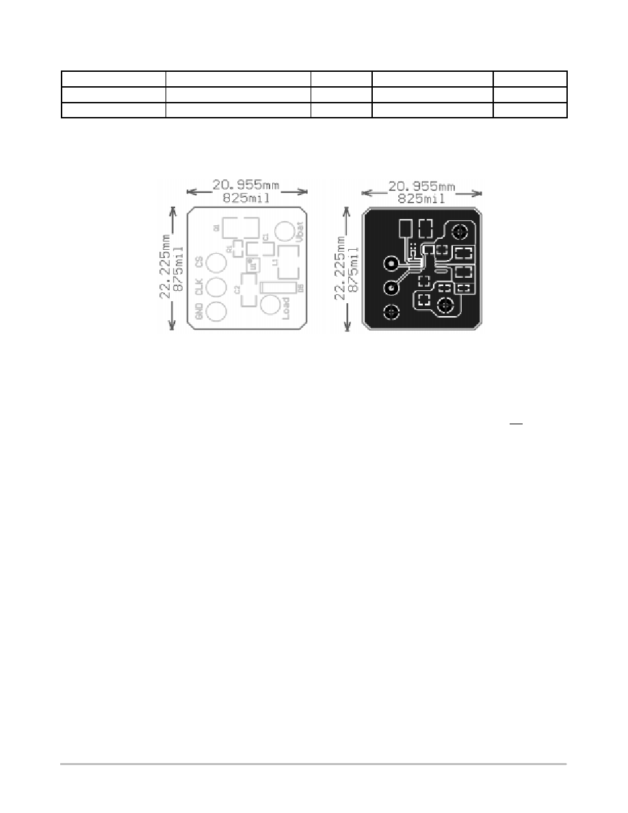
LAYOUT EXAMPLE
Figure 28. Typical Printed Circuit Layout
(the Top Silk Screen and the Top Layer)
The Figure 28 represents the typical printed circuit
layout based on the basic application Figure 1. This
application has been routed on a single copper layer to save
cost. A dual side PCB has better noise protection and can
be the right choice for an industrial system. In order to
avoid voltage spikes, care must be observed to group the
capacitors, the inductor, the Schottky diode and the
integrated circuit in the same area. On the other hand, using
large copper tracks to reduce the resistor connectivity is
strongly recommended.
Obviously, the connectors GND, CLK, CS, V
bat
and
Load are for engineering purpose only and not for final
application.
NCP5008, NCP5009
http://onsemi.com
19
PACKAGE DIMENSIONS
Micro 10
DM SUFFIX
CASE 846B-02
ISSUE B
S
B
M
0.08 (0.003)
A
S
T
DIM
MIN
MAX
MIN
MAX
INCHES
MILLIMETERS
A
2.90
3.10
0.114
0.122
B
2.90
3.10
0.114
0.122
C
0.95
1.10
0.037
0.043
D
0.20
0.35
0.008
0.014
G
0.50 BSC
0.020 BSC
H
0.05
0.15
0.002
0.006
J
0.10
0.21
0.004
0.008
K
4.75
5.05
0.187
0.199
L
0.40
0.70
0.016
0.028
NOTES:
1. DIMENSIONING AND TOLERANCING PER ANSI
Y14.5M, 1982.
2. CONTROLLING DIMENSION: MILLIMETER.
3. DIMENSION A" DOES NOT INCLUDE MOLD
FLASH, PROTRUSIONS OR GATE BURRS. MOLD
FLASH, PROTRUSIONS OR GATE BURRS SHALL
NOT EXCEED 0.15 (0.006) PER SIDE.
4. DIMENSION B" DOES NOT INCLUDE INTERLEAD
FLASH OR PROTRUSION. INTERLEAD FLASH OR
PROTRUSION SHALL NOT EXCEED 0.25 (0.010)
PER SIDE.
5. 846B-01 OBSOLETE. NEW STANDARD 846B-02
-B-
-A-
D
K
G
PIN 1 ID
8 PL
0.038 (0.0015)
-T-
SEATING
PLANE
C
H
J
L

NCP5008, NCP5009
http://onsemi.com
20
ON Semiconductor and are registered trademarks of Semiconductor Components Industries, LLC (SCILLC). SCILLC reserves the right to make
changes without further notice to any products herein. SCILLC makes no warranty, representation or guarantee regarding the suitability of its products for any
particular purpose, nor does SCILLC assume any liability arising out of the application or use of any product or circuit, and specifically disclaims any and all
liability, including without limitation special, consequential or incidental damages. "Typical" parameters which may be provided in SCILLC data sheets and/or
specifications can and do vary in different applications and actual performance may vary over time. All operating parameters, including "Typicals" must be
validated for each customer application by customer's technical experts. SCILLC does not convey any license under its patent rights nor the rights of others.
SCILLC products are not designed, intended, or authorized for use as components in systems intended for surgical implant into the body, or other applications
intended to support or sustain life, or for any other application in which the failure of the SCILLC product could create a situation where personal injury or death
may occur. Should Buyer purchase or use SCILLC products for any such unintended or unauthorized application, Buyer shall indem nify and hold SCILLC and
its officers, employees, subsidiaries, affiliates, and distributors harmless against all claims, costs, damages, and expenses, and reasonable attorney fees
arising out of, directly or indirectly, any claim of personal injury or death associated with such unintended or unauthorized use, even if such claim alleges that
SCILLC was negligent regarding the design or manufacture of the part. SCILLC is an Equal Opportunity/Affirmative Action Employer.
PUBLICATION ORDERING INFORMATION
JAPAN: ON Semiconductor, Japan Customer Focus Center
2-9-1 Kamimeguro, Meguro-ku, Tokyo, Japan 153-0051
Phone: 81-3-5773-3850
ON Semiconductor Website: http://onsemi.com
For additional information, please contact your local
Sales Representative.
NCP5008/D
Literature Fulfillment:
Literature Distribution Center for ON Semiconductor
P.O. Box 5163, Denver, Colorado 80217 USA
Phone: 303-675-2175 or 800-344-3860 Toll Free USA/Canada
Fax: 303-675-2176 or 800-344-3867 Toll Free USA/Canada
Email: orderlit@onsemi.com
N. American Technical Support: 800-282-9855 Toll Free USA/Canada