 | ÐлекÑÑоннÑй компоненÑ: NCP5203 | СкаÑаÑÑ:  PDF PDF  ZIP ZIP |
Äîêóìåíòàöèÿ è îïèñàíèÿ www.docs.chipfind.ru
©
Semiconductor Components Industries, LLC, 2005
January, 2005 - Rev. 1
1
Publication Order Number:
NCP5203/D
NCP5203
2-in-1 DDR Power
Controller
The NCP5203 2-in-1 DDR Power Controller is a complete power
solution for an ACPI compliant high current DDR memory system.
This IC combines the efficiency of a PWM controller for the VDDQ
supply with the simplicity of linear regulator for the VTT
termination voltage. The NCP5203 contains a synchronous PWM
buck controller for driving two external NFETs to form the DDR
memory supply voltage (VDDQ). The
$2.0 A user adjustable VTT
terminator regulator has short circuit protection. An internal power
good function monitors both the VDDQ and VTT outputs and signals
if a fault occurs. Protective features include soft-start, undervoltage
monitoring of 5VDUAL, over protection current (OCP), and thermal
shutdown. The IC is packaged in 18-lead QFN.
Features
·
Supports DDR I and DDR II
·
Incorporates VDDQ, VTT Regulators
·
Operates from Single 5 V Supply
·
VTT Regulator includes Integrated Power FETs Sourcing/Sinking
up to 2.0 A
·
All External Power MOSFETs are N-Channel
·
Adjustable VDDQ
·
Adjustable VTT
·
Fixed Switching Frequency of 300 kHz for VDDQ in S0
·
Fixed Switching Frequency of 600 kHz for VDDQ in S3
·
Soft-Start Protection for VDDQ
·
Undervoltage Monitor of 5VDUAL
·
Short-Circuit Protection for VDDQ and VTT
·
Thermal Shutdown
·
Housed in QFN-18
·
Pb-Free Package is Available*
Typical Applications
·
DDR Memory Supply and Termination Voltage
·
Active Termination Busses (SSTL-2, SSTL-3)
*For additional information on our Pb-Free strategy and soldering details, please
download the ON Semiconductor Soldering and Mounting Techniques Reference
Manual, SOLDERRM/D.
Device
Package
Shipping
ORDERING INFORMATION
NCP5203MNR2
QFN
2500 Tape & Reel
MARKING
DIAGRAM
PIN CONNECTIONS
A
= Assembly Location
WL = Wafer Lot
YY = Year
WW = Work Week
NCP5203
AWLYYWW
18-LEAD QFN, 5 x 6 mm
MN SUFFIX
CASE 505
1
2
3
4
5
6
7
8
9
18
17
16
15
14
13
12
11
10
VDDQEN
VTTEN
PGOOD
REFSNS
FBVTT
AGND
SS
COMP
FBDDQ
VDDQ
VTT
PGND
BST
BGDDQ
TGDDQ
5VDUAL
SWDDQ
OCDDQ
1
18
1
For information on tape and reel specifications,
including part orientation and tape sizes, please
refer to our Tape and Reel Packaging Specifications
Brochure, BRD8011/D
NCP5203MNR2G
QFN
(Pb-Free)
2500 Tape & Reel
http://onsemi.com
NCP5203
http://onsemi.com
2
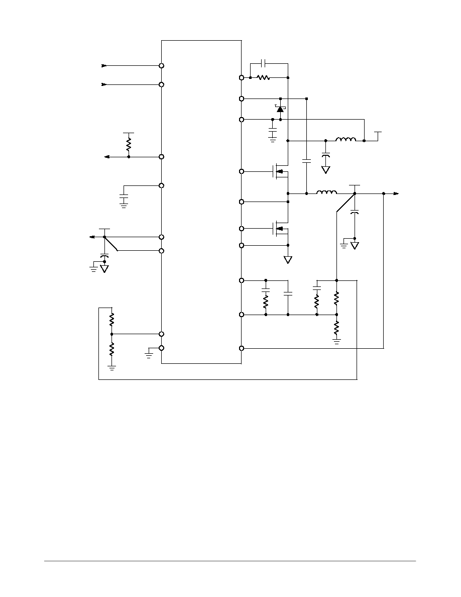
Figure 1. Typical Application Diagram
VTTEN
VTT
1.25 V,
2.0 A Peak
VTT
COUT2
NCP5203
M1
M2
VDDQ
FBDDQ
L
VDDQ
VDDQEN
R3
VTTEN
VDDQEN
5VDUAL
PGOOD
PGOOD
SS
CSS
FBVTT
R4
REFSNS
AGND
CL1
RL1
OCDDQ
BST
5VDUAL
TGDDQ
SWDDQ
BGDDQ
PGND
COMP
CZ1
RZ1
CP1
CZ2
RZ2
R1
R2
5VDUAL
2.5V, 15A
COUT1
NCP5203
http://onsemi.com
3
+
-
PGOOD
BST
OCDDQ
RL1
TGDDQ
M3
BGDDQ
M4
SWDDQ
REFSNS
COMP
VDDQ
FBDDQ
CZ1
CP1
CZ2
R2
R1
L
VDDQ
COUT1
Thermal
Shutdown
VREF
Control
Logic
5VDUAL
VREF
R10
R1
1
5VDUAL
UVLO
PGND
VDDQ
PWM
Logic
INREGVTT
INREGDDQ
OSC
+ -
PWM-
COMP
+
-
+
-
GND
+
-
VTT
Regulation
Control
VTTS0
VTTS3
INREGDDQ
INREGVTT
SC2PWR
SC2GND
A
PGND
5VDUAL
PGND
5VDUAL
M1
M2
PGND
+
-
ILIM
PGND
VBST
IREF
V
oltage and
Current Reference
VREFGD
AMP
VREF
PGND
VBST
RZ1
RZ2
TSD
VTT
FBVTT
VTT
COUT2
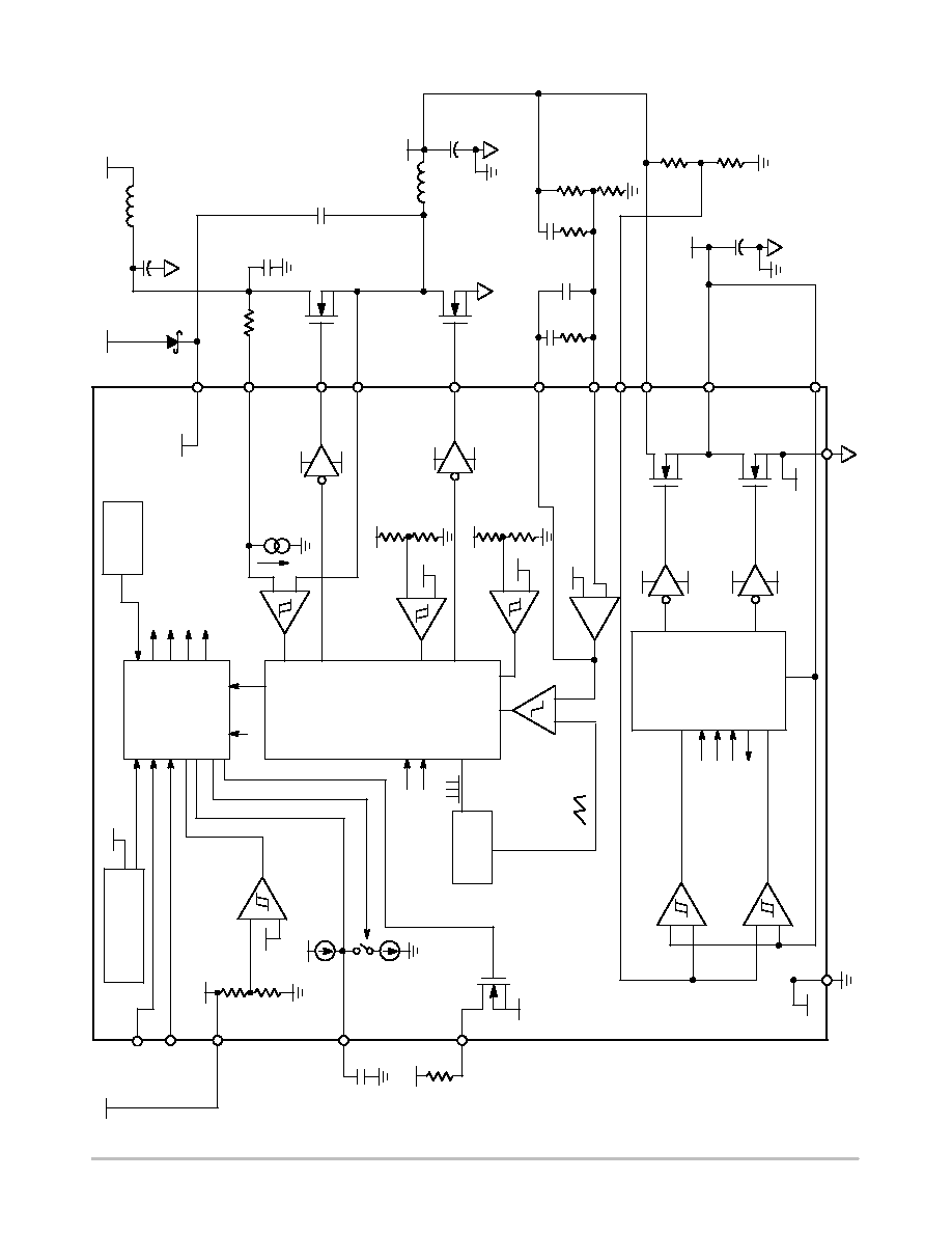
Figure 2. Detailed Block Diagram
VDDQEN
VTTEN
5VDUAL
5VDUAL
VDDQS0
VDDQS3
VTTS0
VTTS3
+
-
+
-
FBDDQ
VREF
VREF
FBDDQ
OVLO
UVLO
R3
R4
PGND
AGND
CDCPL
VBST
5VDUAL
5VDUAL
LIN
CBULK
CBST
5VDUAL
5VDUAL
5VDL GD
F
AUL
T
R14
R15
R16
R17
VDDQS0
VDDQS3
SS
CSS
R5
NCP5203
http://onsemi.com
4
PIN FUNCTION DESCRIPTION
Pin No.
Symbol
Description
1
VDDQEN
VDDQ regulator enable input. Active high.
2
VTTEN
VTT regulator enable input. Active high.
3
PGOOD
Power good signal open-drain output.
4
REFSNS
Reference voltage input of VTT regulator.
5
FBVTT
VTT regulator feedback pin for closed loop regulation.
6
AGND
Analog ground connection and remote ground sense.
7
SS
Soft-start capacitor connection to ground.
8
COMP
VDDQ error amplifier compensation node.
9
FBDDQ
VDDQ regulator feedback pin for closed loop regulation.
10
OCDDQ
Overcurrent sense and program input for the high-side FET of VDDQ regulator.
11
SWDDQ
VDDQ regulator inductor driven node and current limit sense input.
12
5VDUAL
5VDUAL supply input.
13
TGDDQ
Gate driver output for DDQ regulator high-side N-Channel power FET.
14
BGDDQ
Gate driver output for DDQ regulator low-side N-Channel power FET.
15
BST
Supply input of VDDQ regulator and 5 V boost capacitor connection.
16
PGND
Power ground.
17
VTT
VTT regulator output.
18
VDDQ
Power input for VTT regulator.
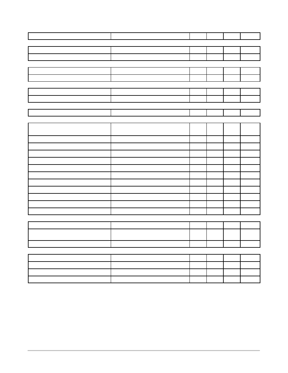
MAXIMUM RATINGS
(Note 1)
Rating
Symbol
Value
Unit
Power Supply Voltage (Pin 12, 18)
5VDUAL
-0.3, 6.5
V
Gate Drive Supply/Output Voltage (Pin 13, 14, 15)
VBST, Vg
-0.3, 14
V
Switch DDQ (Pin 11)
SWDDQ
-1.0, 5VDUAL
V
Input/Output Pins (Pin 1, 2, 7; 4, 5, 17; 3, 8, 9, 10)
V
IO
-0.3, 6.5
V
Thermal Characteristics
QFN-18 Plastic Package
Thermal Resistance Junction-to-Ambient
R
q
JA
35
°
C/W
Operating Junction Temperature Range
T
J
0 to +150
°
C
Operating Ambient Temperature Range
T
A
0 to +70
°
C
Storage Temperature Range
T
stg
-55 to +150
°
C
Moisture Sensitivity Level
MSL
2.0
-
Electro Static Discharge (ESD)
Human Body Model
Machine Model
HBM
MM
2.0
200
kV
V
Maximum ratings are those values beyond which device damage can occur. Maximum ratings applied to the device are individual stress limit values
(not normal operating conditions) and are not valid simultaneously. If these limits are exceeded, device functional operation is not implied, damage
may occur and reliability may be affected.
1. All voltages are with respect to AGND (Pin 6) and PGND (Pin 16).
NCP5203
http://onsemi.com
5
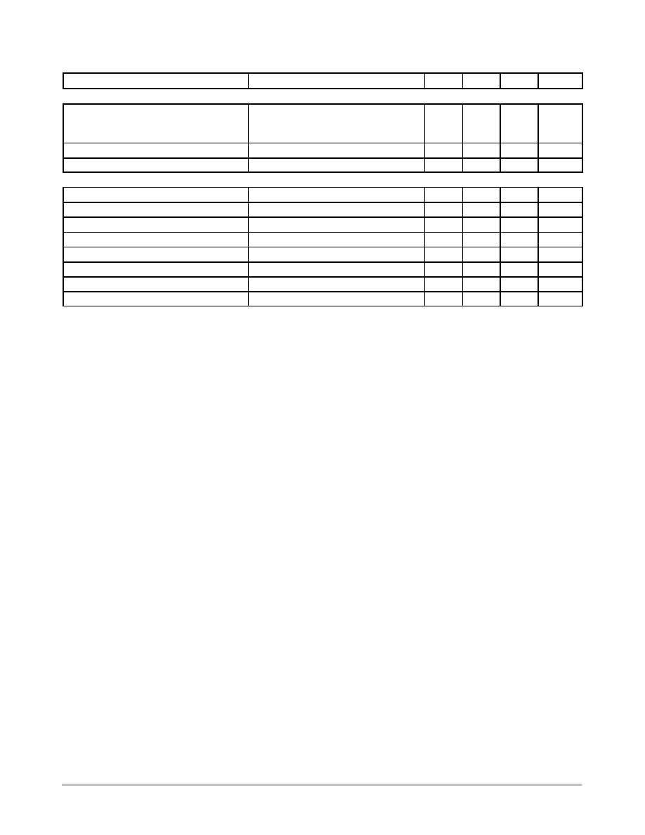
ELECTRICAL CHARACTERISTICS
(5VDUAL = 5.0 V, T
A
= 0 to 70
°
C)
Characteristic
Test Conditions
Min
Typ
Max
Unit
Supply Voltage
5VDUAL Operating Voltage
-
4.5
5.0
5.5
V
BST Operating Voltage
-
4.0
10
13.2
V
Supply Current
Quiescent Supply Current (5VDUAL)
-
-
5.0
10
mA
Shutdown Current
VDDQEN = 0 V, VTTEN = 0 V
-
-
1.0
mA
Undervoltage Monitor
5VDUAL UVLO Lower Threshold
Falling Edge
3.6
3.95
4.3
V
5VDUAL UVLO Hysteresis
-
-
0.2
-
V
Thermal Shutdown
Thermal Trip Point
(Note 2)
-
150
-
_
C
VDDQ Switching Regulator
FBDDQ Feedback Voltage,
Control Loop in Regulation
T
A
= 0 to 70
_
C
T
A
= 25
_
C
1.225
1.232
1.25
1.25
1.275
1.268
V
Feedback Input Current
VFBDDQ = 1.25 V
-
-
1.0
m
A
Oscillator Frequency in S0 Mode
VDDQEN = VTTEN = 5 V
262.5
300
337.5
kHz
Oscillator Frequency in S3 Mode
VDDQEN = 5 V, VTTEN = 0 V
500
600
700
kHz
Ramp-Amplitude Voltage
At Max Duty Cycle
-
1.25
-
V
OCDDQ Pin Current Sink
VOCDDQ = 4.0 V, T
A
= 25
_
C
23
35
47
m
A
OCDDQ Pin Current Sink Temperature Coefficient
(Note 2)
-
3200
-
ppm/
_
C
Minimum Duty Cycle
-
0
-
-
%
Maximum Duty Cycle
-
-
90
-
%
Soft-start Current
DDQEN = 5.0 V; V
SS
= 0 V
3.5
5.0
6.5
m
A
Overvoltage Trip Threshold
With respect to Error Comparator Threshold
115
130
-
%
Undervoltage Trip Threshold
With respect to Error Comparator Threshold
-
65
75
%
Error Amplifier
DC Gain
(Note 2)
-
70
-
dB
Unity Gain Bandwidth
COMP_GND = 220 nF, 1.0
W
in series
(Note 2)
-
2.0
-
MHz
Slew Rate
COMP_GND = 10 pF (Note 2)
-
8.0
-
V/
m
S
Gate Drivers
TGDDQ Gate Pull-HIGH Resistance
I
OUT
= 400 mA, VBST = 10 V
-
3.5
-
W
TGDDQ Gate Pull-LOW Resistance
I
OUT
= 400 mA, VBST = 10 V
-
2.5
-
W
BGDDQ Gate Pull-HIGH Resistance
I
OUT
= 400 mA, VBST = 10 V
-
3.5
-
W
BGDDQ Gate Pull-LOW Resistance
I
OUT
= 400 mA, VBST = 10 V
-
1.3
-
W
2. Guaranteed by design, not tested in production.
NCP5203
http://onsemi.com
6
ELECTRICAL CHARACTERISTICS (continued)
(5VDUAL = 5.0 V, T
A
= 0 to 70
°
C)
Characteristic
Test Conditions
Min
Typ
Max
Unit
VTT Active Terminator
VTT with Respect to REFSNS
REFSNS VTT,
IOUT = 0 to 2.0 A (Sink Current)
IOUT = 0 to 2.0 A (Source Current)
-30
-
-
-
-
30
mV
Source Current Limit
-
-
-2.5
-2.05
A
Sink Current Limit
-
2.05
2.75
-
A
Control Section
VDDQEN Pin Threshold High
-
1.4
-
-
V
VDDQEN Pin Threshold Low
-
-
-
0.5
V
VDDQEN Pin Input Current
VDDQEN = 5 V
-
5.0
-
m
A
VTTEN Pin Threshold High
-
1.4
-
-
V
VTTEN Pin Threshold Low
-
-
-
0.5
V
VTTEN Pin Input Current
VDDQEN = VTTEN = 5 V
-
5.0
-
m
A
PGOOD Pin ON Resistance
I_PGOOD = 5.0 mA
-
80
-
W
PGOOD Pin OFF Current
-
-
-
1.0
m
A
NCP5203
http://onsemi.com
7
DETAILED OPERATING DESCRIPTION
General
The NCP5203
2-in-1 DDR Power Controller combines
the efficiency of a VDDQ PWM controller with the
simplicity of a linear regulator for VTT termination. Both
VDDQ and VTT outputs can be user adjusted.
The inclusion of both VDDQ and VTT power good
voltage monitors, soft-start, VDDQ overvoltage and
undervoltage detection, supply undervoltage monitors, and
thermal shutdown, makes this device a total power solution
for high current DDR memory systems.
VDDQ Switching Regulator in Normal (S0) Mode
The VDDQ regulator is a switching synchronous
rectification buck controller directly driving two external
N-Channel power FETs. An external resistor divider sets
the nominal output voltage. The control architecture is
voltage mode fixed frequency PWM (300 kHz
±
12.5%)
with external compensation. The VDDQ output voltage is
divided down and fed back to the inverting input of an
internal amplifier through the FBDDQ pin to close the loop
at VDDQ = VFBDDQ
×
(1 + R2/R1). This amplifier
compares the feedback voltage with an internal VREF1
(= 1.25 V) to generate an error signal for the PWM
comparator. This error signal is further compared with a
fixed frequency Ramp waveform derived from the internal
oscillator to generate a pulse-width-modulated signal.
This PWM signal drives the external N-Channel Power
FETs via the TGDDQ and BGDDQ pins. External inductor
L and capacitor COUT1 filter the output. The VDDQ
output voltage ramps up at a pre-defined soft-start rate
each time the IC exits S5. When in normal mode, and
regulation of VDDQ is detected, signal INREGDDQ will
go high to notify the control logic block.
For enhanced efficiency, an active synchronous switch is
used to eliminate the conduction loss contributed by the
forward voltage of a diode or Schottky diode rectifier.
Adaptive non-overlap timing control of the
complementary gate drive output signals is provided to
reduce shoot-through current.
Tolerance of VDDQ
The tolerance of VFBDDQ and the ratio of the external
resistor divider R2/R1 both impact the precision of VDDQ.
When the control loop is in regulation, VDDQ = VFBDDQ
×
(1 + R2/R1). With a worst case (overtemperature)
VFBDDQ tolerance of
±
2%, a worst case range of 2.5% for
VDDQ will be assured if the ratio R2/R1 is specified as
0.98985
±
1%.
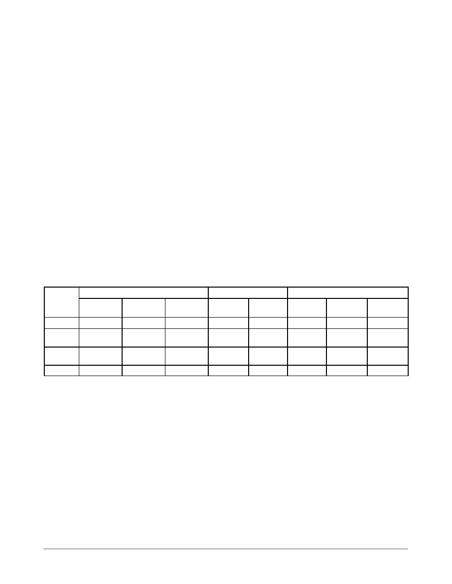
Table 1. State, Operation, Input and Output Condition Table
USER INPUTS
OPERATING CONDITIONS
OUTPUT CONDITIONS
MODE
5VDUAL
UVLO
VDDQEN
VTTEN
VDDQ
VTT
TGDDQ
BGDDQ
PGOOD
S5
Low
X
X
H-Z
H-Z
Low
Low
Low
S0
High
High
High
Normal
Normal
Normal
(300 kHz)
Normal
(300 kHz)
H-Z
S3
High
High
Low
Standby
H-Z
Normal
(600 kHz)
Low
Low
S5
High
Low
X
H-Z
H-Z
Low
Low
Low
VDDQ Regulator in Standby Mode (S3)
During S3, the VDDQ regulator operates in
asynchronous switch mode. The switching frequency is
increased to 600 kHz, the low-side FET is disabled, and the
body diode of the low side FET is used. The regulator will
operate in discontinuous conduction mode (DCM) and the
switching frequency is doubled to reduce peak conduction
current.
VDDQ Regulator Fault Protection
During S0 and S3, the external resistor (RL1) sets the
current limit for the high-side switch. An internal 35
mA
current sink at OCDDQ pin establishes a voltage drop
across this resistor. This voltage is compared to the voltage
at SWDDQ pin when the TGDDQ is high after a fixed
blanking period of 500 ns to avoid false current limit
triggering. When the voltage at SWDDQ is lower than
OCDDQ, an overcurrent condition occurs, upon which all
outputs will be latched off to protect against a
short-to-ground condition on SWDDQ or VDDQ. The IC
will be reset once 5VDUAL or VDDQEN is cycled.
VDDQ Regulator Feedback Compensation
The recommended compensation network is shown in
Figure 2.

NCP5203
http://onsemi.com
8
VTT Active Terminator in Normal Mode (S0)
The VTT active terminator is a two-quadrant linear
regulator with two internal N-channel power FETs to
provide transient current sink and source capability up to
2.0 A. It is activated in normal mode in S0 when the
VTTEN pin is high and VDDQ is in regulation. When in the
S0 state and VTT is in regulation, signal INREGVTT will
go high to notify the control logic block. The VTT regulator
is powered from VDDQ with the internal FET's gate drive
power derived from 5VDUAL. The VTT output voltage
can be adjusted by using an external resistor divider
connected to the REFSNS pin. This regulator is stable with
any value of output capacitor greater than 470
mF, and is
insensitive to ESR ranging from 2.0 m
W to 400 mW.
VTT Active Terminator in Normal Mode (S3)
VTT output is high-impedance in S3 mode.
VTT Active Terminator Fault Protection
To provide protection for the internal FETs,
bi-directional current limit is implemented, preset at 2.4 A
magnitude. This current limit is also used as constant
current source during VTT startup.
VTT Active Terminator Thermal Consideration
The VTT terminator is designed to handle large transient
output currents. If large currents are required for very long
duration, then care should be taken to ensure the maximum
junction temperature is not exceed. The 5x6 QFN-18 has
a thermal resistance of 35
_C/W (dependent on air flow,
grade of copper, and number of vias). In order to take full
advantage of this thermal capability, the thermal pad
underneath must be soldered directly to a PCB metal
substrate.
Supply Voltages Undervoltage Monitor
The IC continuously monitors 5VDUAL through the
5VDUAL pin. 5VDLGD is set high if 5VDUAL is higher
than its preset threshold (derived from VREF with
hysteresis). The IC will later latch off if 5VDUAL is in S0
providing both VDDQEN and VTTEN remain high.
Thermal Shutdown
If the chip junction temperature exceeds 150
_C, the
entire IC will shutdown. The IC resumes normal operation
only after 5VDUAL or VDDQEN is cycled.
NCP5203
http://onsemi.com
9
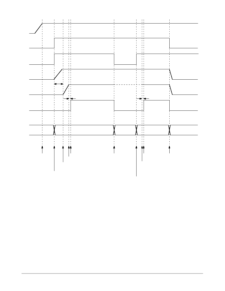
5VDUAL
VDDQEN
VTTEN
VDDQ
VTT
PGOOD
OPERATING
MODE
Soft
Start
10ms
t
hold
200
m
s
VTT in H-Z
t
hold
200
m
s
S0
S3
S0
S5
5VDUAL
comes out
of UVLO
VDDQEN goes
HIGH, VDDQ is
activated. VTTEN
goes HIGH, VTT is
not activated until
VDDQ is Good.
INREGDDQ goes HIGH,
VTT goes into normal mode.
PGOOD goes HIGH.
VTTEN goes LOW to
activate S3 mode and
to turn off VTT, then
INREGVTT goes LOW,
PGOOD goes LOW.
PGOOD goes
HIGH.
Both VDDQEN and
VTTEN go LOW to
trigger S5 mode; VDDQ
and VTT is disabled,
then INREGDDQ and
INREGVTT go LOW,
PGOOD goes LOW.
VTTEN goes HIGH,
VTT goes into
normal mode.
Figure 3. Powerup and Powerdown Timing Diagram
S5
VTTEN IS
DON'T CARE
IN S5
INREGVTT goes HIGH.
INREGVTT
goes HIGH.
NCP5203
http://onsemi.com
10
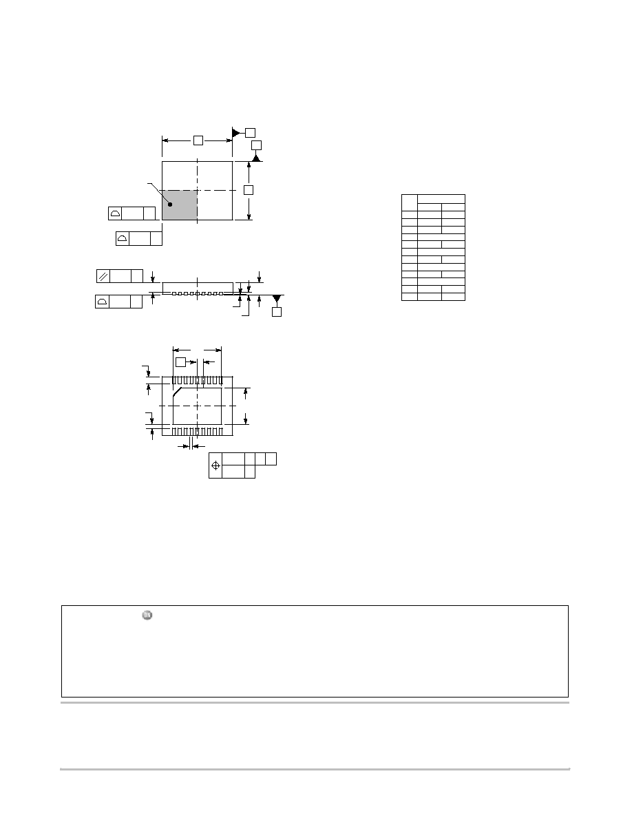
18-LEAD QFN, 5 x 6 mm
MN SUFFIX
CASE 505-01
ISSUE A
C
0.15
E2
D2
L
b
18 X
A
D
NOTES:
1. DIMENSIONS AND TOLERANCING PER
ASME Y14.5M, 1994.
2. DIMENSIONS IN MILLIMETERS.
3. DIMENSION b APPLIES TO PLATED
TERMINALS AND IS MEASURED BETWEEN
0.25 AND 0.30 MM FROM TERMINAL
4. COPLANARITY APPLIES TO THE EXPOSED
PAD AS WELL AS THE TERMINALS.
E
C
e
A
B
DIM
MIN
MAX
MILLIMETERS
A
0.80
1.00
A1
0.00
0.05
A2
0.65
0.75
A3
0.20 REF
b
0.23
0.28
D
6.00 BSC
D2
3.98
4.28
E
5.00 BSC
E2
2.98
3.28
e
0.50 BSC
K
0.20
---
L
0.50
0.60
C
0.15
PIN 1 LOCATION
A1
A3
REF
SEATING
PLANE
C
0.08
C
0.10
A2
18 X
K
18 X
A
0.10
B
C
0.05 C
NOTE 3
1
9
10
18
ON Semiconductor and are registered trademarks of Semiconductor Components Industries, LLC (SCILLC). SCILLC reserves the right to make changes without further notice
to any products herein. SCILLC makes no warranty, representation or guarantee regarding the suitability of its products for any particular purpose, nor does SCILLC assume any
liability arising out of the application or use of any product or circuit, and specifically disclaims any and all liability, including without limitation special, consequential or incidental
damages. "Typical" parameters which may be provided in SCILLC data sheets and/or specifications can and do vary in different applications and actual performance may vary over
time. All operating parameters, including "Typicals" must be validated for each customer application by customer's technical experts. SCILLC does not convey any license under
its patent rights nor the rights of others. SCILLC products are not designed, intended, or authorized for use as components in systems intended for surgical implant into the body,
or other applications intended to support or sustain life, or for any other application in which the failure of the SCILLC product could create a situation where personal injury or death
may occur. Should Buyer purchase or use SCILLC products for any such unintended or unauthorized application, Buyer shall indemnify and hold SCILLC and its officers, employees,
subsidiaries, affiliates, and distributors harmless against all claims, costs, damages, and expenses, and reasonable attorney fees arising out of, directly or indirectly, any claim of
personal injury or death associated with such unintended or unauthorized use, even if such claim alleges that SCILLC was negligent regarding the design or manufacture of the part.
SCILLC is an Equal Opportunity/Affirmative Action Employer. This literature is subject to all applicable copyright laws and is not for resale in any manner.
PUBLICATION ORDERING INFORMATION
N. American Technical Support: 800-282-9855 Toll Free
USA/Canada
Japan: ON Semiconductor, Japan Customer Focus Center
2-9-1 Kamimeguro, Meguro-ku, Tokyo, Japan 153-0051
Phone: 81-3-5773-3850
NCP5203/D
LITERATURE FULFILLMENT:
Literature Distribution Center for ON Semiconductor
P.O. Box 61312, Phoenix, Arizona 85082-1312 USA
Phone: 480-829-7710 or 800-344-3860 Toll Free USA/Canada
Fax: 480-829-7709 or 800-344-3867 Toll Free USA/Canada
Email: orderlit@onsemi.com
ON Semiconductor Website: http://onsemi.com
Order Literature: http://www.onsemi.com/litorder
For additional information, please contact your
local Sales Representative.