
©
Semiconductor Components Industries, LLC, 2004
June, 2004 - Rev. 4
1
Publication Order Number:
NCP5426/D
NCP5426
LDO Regulator/Vibration
Motor Driver
The NCP5426 series of fixed output, 150 mA low dropout linear
regulators are designed to be an economical solution for a variety of
applications. Each device contains a voltage reference unit, an error
amplifier, a PNP power transistor, resistors for setting output voltage,
an under voltage lockout on the input, an enable pin, and current limit
and temperature limit protection circuits.
The NCP5426 is designed for driving a vibration motor using
ceramic capacitors on the output. The device is housed in the
micro-miniature TSOP-5 surface mount package. The NCP5426 is
available in output voltages of 1.2 V to 2.0 V in 0.1 V increments.
Features
∑
Wide Operating Voltage Range to 12 V
∑
Internally Set Output Voltages
∑
Enable Pin for On/Off Control
∑
UVLO on the Input Voltage with Hysteresis
∑
Current and Thermal Protection
∑
Compatible with Ceramic, Tantalum or Aluminum Electrolytic
Capacitors
∑
Pb-Free Package is Available
Typical Applications
∑
Vibration Motor Driver
Driver w/
Current
Limit
V
in
V
out
Thermal
Shutdown
Enable
GND
OFF
ON
5
1
4
2
Figure 1. Internal Schematic
UVLO
This device contains 47 active transistors.
See detailed ordering and shipping information in the package
dimensions section on page 7 of this data sheet.
ORDERING INFORMATION
TSOP-5
SN SUFFIX
CASE 483
PIN CONNECTIONS AND
MARKING DIAGRAM
1
3
V
out
Enable
2
GND
N/C
4
V
in
5
xxxYW
xxx = Version
Y
= Year
W = Work Week
(Top View)
1
5
http://onsemi.com
NCP5426
http://onsemi.com
2
¡¡¡¡¡¡¡¡¡¡¡¡¡¡¡¡¡¡¡¡¡¡¡¡¡¡¡¡¡¡¡¡¡
¡¡¡¡¡¡¡¡¡¡¡¡¡¡¡¡¡¡¡¡¡¡¡¡¡¡¡¡¡¡¡¡¡
DETAILED PIN DESCRIPTION
¡¡¡¡¡
¡¡¡¡¡
Pin
¡¡¡¡¡¡¡
¡¡¡¡¡¡¡
Name
¡¡¡¡¡¡¡¡¡¡¡¡¡¡¡¡¡¡¡¡¡¡¡
¡¡¡¡¡¡¡¡¡¡¡¡¡¡¡¡¡¡¡¡¡¡¡
Description
¡¡¡¡¡
¡
¡¡¡
¡
¡¡¡¡¡
1
¡¡¡¡¡¡¡
¡
¡¡¡¡¡
¡
¡¡¡¡¡¡¡
Enable
¡¡¡¡¡¡¡¡¡¡¡¡¡¡¡¡¡¡¡¡¡¡¡
¡
¡¡¡¡¡¡¡¡¡¡¡¡¡¡¡¡¡¡¡¡¡
¡
¡¡¡¡¡¡¡¡¡¡¡¡¡¡¡¡¡¡¡¡¡¡¡
The enable pin allows the user to control the output. A low signal disables the output and places
the device into a low current standby mode.
¡¡¡¡¡
¡¡¡¡¡
2
¡¡¡¡¡¡¡
¡¡¡¡¡¡¡
GND
¡¡¡¡¡¡¡¡¡¡¡¡¡¡¡¡¡¡¡¡¡¡¡
¡¡¡¡¡¡¡¡¡¡¡¡¡¡¡¡¡¡¡¡¡¡¡
Ground pin.
¡¡¡¡¡
¡¡¡¡¡
3
¡¡¡¡¡¡¡
¡¡¡¡¡¡¡
N/C
¡¡¡¡¡¡¡¡¡¡¡¡¡¡¡¡¡¡¡¡¡¡¡
¡¡¡¡¡¡¡¡¡¡¡¡¡¡¡¡¡¡¡¡¡¡¡
This pin is not connected to the device.
¡¡¡¡¡
¡¡¡¡¡
4
¡¡¡¡¡¡¡
¡¡¡¡¡¡¡
V
out
¡¡¡¡¡¡¡¡¡¡¡¡¡¡¡¡¡¡¡¡¡¡¡
¡¡¡¡¡¡¡¡¡¡¡¡¡¡¡¡¡¡¡¡¡¡¡
Regulated output voltage.
¡¡¡¡¡
¡¡¡¡¡
5
¡¡¡¡¡¡¡
¡¡¡¡¡¡¡
V
in
¡¡¡¡¡¡¡¡¡¡¡¡¡¡¡¡¡¡¡¡¡¡¡
¡¡¡¡¡¡¡¡¡¡¡¡¡¡¡¡¡¡¡¡¡¡¡
Input voltage.
MAXIMUM RATINGS
Rating
Symbol
Value
Unit
¡¡¡¡¡¡¡¡¡¡¡¡¡¡¡¡
¡¡¡¡¡¡¡¡¡¡¡¡¡¡¡¡
Max Voltage, All Pins
¡¡¡¡¡¡
¡¡¡¡¡¡
V
MAX
¡¡¡¡¡¡¡¡¡¡
¡¡¡¡¡¡¡¡¡¡
12
¡¡¡¡
¡¡¡¡
V
¡¡¡¡¡¡¡¡¡¡¡¡¡¡¡¡
¡¡¡¡¡¡¡¡¡¡¡¡¡¡¡¡
Power Dissipation to Air
¡¡¡¡¡¡
¡¡¡¡¡¡
P
A
¡¡¡¡¡¡¡¡¡¡
¡¡¡¡¡¡¡¡¡¡
150
¡¡¡¡
¡¡¡¡
mW
¡¡¡¡¡¡¡¡¡¡¡¡¡¡¡¡
¡¡¡¡¡¡¡¡¡¡¡¡¡¡¡¡
Power Dissipation, Board Mounted
¡¡¡¡¡¡
¡¡¡¡¡¡
P
¡¡¡¡¡¡¡¡¡¡
¡¡¡¡¡¡¡¡¡¡
600
¡¡¡¡
¡¡¡¡
mW
¡¡¡¡¡¡¡¡¡¡¡¡¡¡¡¡
¡¡¡¡¡¡¡¡¡¡¡¡¡¡¡¡
Operating and Storage Temperature
¡¡¡¡¡¡
¡¡¡¡¡¡
T
A
¡¡¡¡¡¡¡¡¡¡
¡¡¡¡¡¡¡¡¡¡
-40 to 85
¡¡¡¡
¡¡¡¡
∞
C
¡¡¡¡¡¡¡¡¡¡¡¡¡¡¡¡
¡¡¡¡¡¡¡¡¡¡¡¡¡¡¡¡
Thermal Resistance
¡¡¡¡¡¡
¡¡¡¡¡¡
T
JA
¡¡¡¡¡¡¡¡¡¡
¡¡¡¡¡¡¡¡¡¡
300
¡¡¡¡
¡¡¡¡
∞
C/W
Junction Temperature
T
J
125
∞
C
Maximum ratings are those values beyond which device damage can occur. Maximum ratings applied to the device are individual stress limit
values (not normal operating conditions) and are not valid simultaneously. If these limits are exceeded, device functional operation is not implied,
damage may occur and reliability may be affected.
ELECTRICAL CHARACTERISTICS
(T
A
= 25
∞
C, for min/max values T
A
is the operating junction temperature that
applies, V
CC
= 3.5 V, unless otherwise noted)
Characteristic
Symbol
Min
Typ
Max
Unit
Operating Voltage
V
CC
-
-
12
V
Operating Voltage Turn On, I
out
= 30 mA, Increasing V
CC
V
CCON
-
2.6
2.8
V
Operating Voltage Turn Off, I
out
= 30 mA, Decreasing V
CC
V
CCOFF
2.0
2.1
2.2
V
Operating Voltage Hysteresis, I
out
= 30 mA
V
CC(hyst)
400
500
600
mV
Operating Current No Load
I
CC
-
120
240
m
A
Operating Current, V
CC
= 1.8 V, Enable High
I
CC(uvlo)
-
80
160
m
A
Operating Current, Enable Low
I
CC(off)
-
-
0.1
m
A
Maximum Output Current, V
out
= 0.95 *V
nom
I
out(max)
150
-
-
mA
Overcurrent Protection, V
out
= 0 V
I
out(limit)
-
270
-
mA
Load Regulation, V
in
= 3.5 V, I
out
1.0 to 100 mA
Reg
load
-
30
60
mV
Line Regulation, I
out
= 30 mA, V
in
3.0 to 5.0 V
Reg
line
-
10
20
mV
Ripple Rejection, V
in
3.5 V, f 120 Hz, V
pp
1.0 V, I
out
30 mA
RR
55
70
-
dB
Temperature Shutdown
T
std
-
150
-
∞
C
V
CC
Low Detector Temperature Coefficient, I
out
= 30 mA,
T = -40 to 85
∞
C
D
V
CC
H to L/
D
T
-
200
-
ppm/
∞
C
V
out
Temperature Coefficient
D
V
o
/
D
T
-
100
-
ppm/
∞
C
Enable Pin High Threshold
V
eh
1.6
-
-
V
Enable Pin Low Threshold
V
el
-
-
0.4
V
Enable Pin Current, V
e
= 1.6 V
l
e
-
5.0
10
m
A
-1.3 V
Output Voltage, I
out
= 30 mA
V
out
1.261
1.3
1.339
V
NCP5426
http://onsemi.com
3
100
80
70
60
50
100 k
10 k
40
30
20
10
0
1 k
1 M
FREQUENCY (Hz)
RIPPLE REJECTION (dB)
90
0.8
0
12
75
0
50
25
LOAD REGULA
TION (mV)
-20
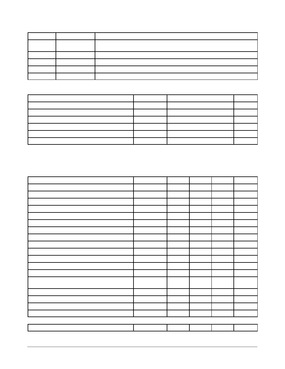
Figure 2. Load Regulation NCP5426
Figure 3. Current Limit NCP5426
OUTPUT CURRENT (mA)
OUTPUT VOL
T
AGE (V)
20
0
200
250
150
100
300
50
0.4
1.0
0.2
0.6
0
1.2
1.4
OUTPUT CURRENT (mA)
4
8
16
100
150
-4
-8
-12
-16
125
-50
136
50
130
0
QUIESCENT CURRENT (
m
A)
118
TEMPERATURE (
∞
C)
Figure 4. Quiescent Current vs. Temperature
Figure 5. Undervoltage Lockout vs.
Temperature
140
TEMPERATURE (
∞
C)
132
134
138
100
125
128
126
124
122
120
Figure 6. Ripple Rejection vs. Frequency
V
in
= 3.5 V
V
out
= 1.3 V
I
out
= 1.0 mA
C
out
= 1.0
m
F
V
e
= 2.5 V
V
in
= 3.5 V
I
out
= 0 mA
V
out(nom)
= 1.3 V
V
e
= V
in
V
in
= 3.5 V
V
e
= 2.5 V
V
out(nom)
= 1.3 V
V
in
= 3.5 V
V
e
= 2.5 V
V
out
= 1.3 V
C
out
= 1.0
m
F
-50
2.7
125
2.4
60
10
UVLO (V)
2.0
2.5
2.6
2.3
2.2
2.1
V
th
ON
V
th
OFF
-25
25
75
0
150
TIME (
m
s)
OUTPUT VOL
T
AGE
DEVIA
TION (mV)
100
200
700
300 400
500
600
800
900
I
out
, OUTPUT
CURRENT (mA)
I
out
= 1 mA to 150 mA
V
in
= 3.5 V
V
out
= 1.3 V
C
in
= 4.7
m
F
C
out
= 4.7
m
F
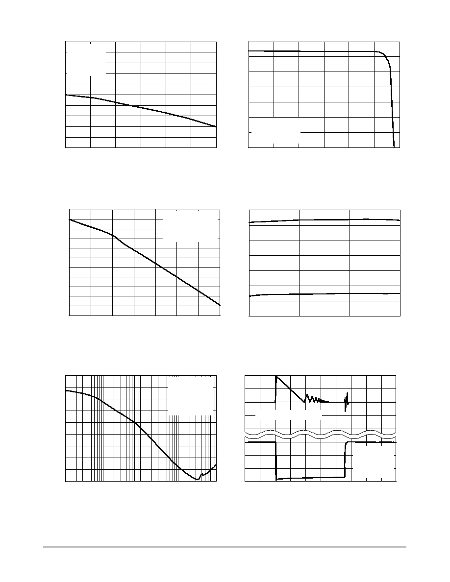
Figure 7. Load Transient Response
1000
50
0
NCP5426
http://onsemi.com
4
7.00
6.50
6.25
6.75
6.00
3.75
ENABLE
CURRENT (
m
A)
3.00
TEMPERATURE (
∞
C)
Figure 8. Enable Current vs. Temperature
Figure 9. Enable Current vs. Temperature
ENABLE
CURRENT (
m
A)
TEMPERATURE (
∞
C)
4.00
3.50
3.25
-50
50
0
100
50
0
-50
V
in
= 3.5 V
V
e
= 1.6 V
I
out
= 30 mA
V
in
= 3.5 V
V
e
= 2.5 V
I
out
= 30 mA
-25
75
125
100
-25
75
125
3
0.70
12
0.40
9
6
LINE REGULA
TION (mV)
0
Figure 10. Line Regulation
0.90
V
in
(V)
0.50
0.60
0.80
0.30
0.20
0.10
V
out
= 1.3 V
I
out
= 30 mA
C
out
= 1
m
F
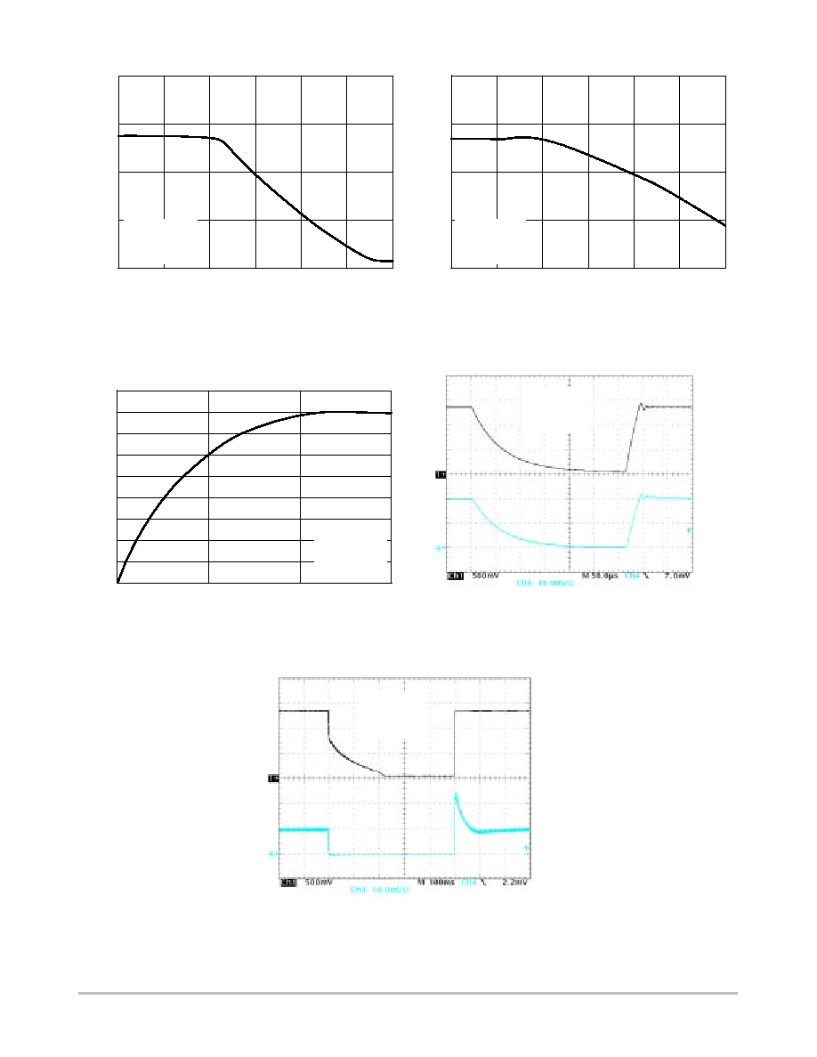
Figure 11. Resistive Transient Response for
Switching the Enable Pin, R
out
- 13 Ohms
Figure 12. Transient Response for Switching
the Enable Pin, Vibration Motor Load
C
in
= C
out
= 4.7
m
F
C
in
= C
out
= 4.7
m
F
V
in
= 3.5 V
V
out
= 1.3 V
100 ms/div
1.3 V
0
V
out
50 mA
0 mA
I
out
V
in
= 3.5 V
V
out
= 1.3 V
50
m
s/div
1.3 V
0
V
out
100 mA
0
I
out

NCP5426
http://onsemi.com
5
DEFINITIONS
Load Regulation
The change in output voltage for a change in output load
current at a constant temperature and input voltage.
Dropout Voltage
The input/output differential at which the regulator output
no longer maintains regulation against further reductions in
input voltage. Measured when the output drops 2.0% below
its nominal. The junction temperature, load current, and
minimum input supply requirements affect the dropout level.
Output Noise Voltage
This is the integrated value of the output noise over a
specified frequency range. Input voltage and output load
current are kept constant during the measurement. Results
are expressed in
mVRMS or nV
Hz.
Quiescent Current
The current which flows through the ground pin when the
regulator operates without a load on its output: internal IC
operation, bias, etc. When the LDO becomes loaded, this
term is called the Ground current. It is actually the difference
between the input current (measured through the LDO input
pin) and the output current.
Line Regulation
The change in output voltage for a change in input voltage.
The measurement is made under conditions of low
dissipation or by using pulse technique such that the average
chip temperature is not significantly affected.
Line Transient Response
Typical over and undershoot response when input voltage
is excited with a given slope.
Thermal Protection
Internal thermal shutdown circuitry is provided to protect
the integrated circuit in the event that the maximum junction
temperature is exceeded. When activated at typically 150
∞
C,
the regulator turns off. This feature is provided to prevent
failures from accidental overheating.
Maximum Package Power Dissipation
The power dissipation level at which the junction
temperature reaches its maximum operating value, i.e.
125
∞
C.