1
Publication Order Number:
NCP552/D
©
Semiconductor Components Industries, LLC, 2004
September, 2004 - Rev. 5
NCP552, NCP553, NCV553
80 mA CMOS Low Iq
NOCAPE Voltage Regulator
This series of fixed output NOCAP linear regulators are designed
for handheld communication equipment and portable battery powered
applications which require low quiescent. This series features an
ultra-low quiescent current of 2.8
mA. Each device contains a voltage
reference unit, an error amplifier, a PMOS power transistor, resistors
for setting output voltage, current limit, and temperature limit
protection circuits. The NCP552 series provides an enable pin for
ON/OFF control.
These voltage regulators have been designed to be used with low
cost ceramic capacitors. The devices have the ability to operate
without an output capacitor. The devices are housed in the
micro-miniature SC82-AB surface mount package. Standard voltage
versions are 1.5, 1.8, 2.5, 2.7, 2.8, 3.0, 3.3, and 5.0 V. Other voltages
are available in 100 mV steps.
Features
∑
Pb-Free Packages are Available*
∑
Low Quiescent Current of 2.8
mA Typical
∑
Low Output Voltage Option
∑
Output Voltage Accuracy of 2.0%
∑
Industrial Temperature Range of -40
∞
C to 85
∞
C
(NCV553, T
A
= -40
∞
C to +125
∞
C)
∑
NCP552 Provides an Enable Pin
Typical Applications
∑
Battery Powered Consumer Products
∑
Hand-Held Instruments
∑
Camcorders and Cameras
∑
NCV Prefix for Automotive and Other Applications Requiring Site
and Control Changes
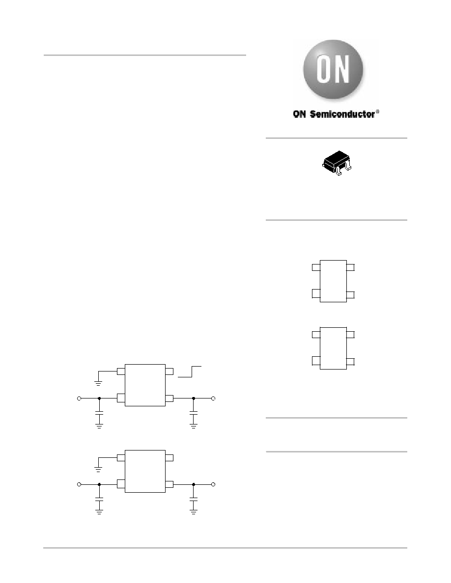
Figure 1. NCP552 Typical Application Diagram
This device contains 32 active transistors
Output
C2
OFF
ON
+
Input
GND Enable
V
in
V
out
+
C1
Figure 2. NCP553 Typical Application Diagram
Output
C2
+
Input
GND
N/C
V
in
V
out
+
C1
This device contains 32 active transistors
SC82-AB (SC70-4)
SQ SUFFIX
CASE 419C
1
4
PIN CONNECTIONS &
MARKING DIAGRAMS
GND
(NCP552 Top View)
1
2
4
3
V
in
Enable
V
out
xxxM
xxx = Device Code
M
= Date Code
GND 1
2
4
3
V
in
N/C
V
out
xxxM
(NCP553, NCV553 Top View)
See detailed ordering and shipping information in the package
dimensions section on page 8 of this data sheet.
ORDERING INFORMATION
http://onsemi.com
*For additional information on our Pb-Free strategy
and soldering details, please download the
ON Semiconductor Soldering and Mounting
Techniques Reference Manual, SOLDERRM/D.
http://onsemi.com

NCP552, NCP553, NCV553
http://onsemi.com
2
¡¡¡¡¡¡¡¡¡¡¡¡¡¡¡¡¡¡¡¡¡¡¡¡¡¡¡¡¡¡¡¡¡
¡¡¡¡¡¡¡¡¡¡¡¡¡¡¡¡¡¡¡¡¡¡¡¡¡¡¡¡¡¡¡¡¡
PIN FUNCTION DESCRIPTION
¡¡¡¡
¡¡¡¡
NCP552
¡¡¡¡
¡¡¡¡
NCP553
¡¡¡¡
¡¡¡¡
Pin Name
¡¡¡¡¡¡¡¡¡¡¡¡¡¡¡¡¡¡¡¡¡¡¡¡
¡¡¡¡¡¡¡¡¡¡¡¡¡¡¡¡¡¡¡¡¡¡¡¡
Description
¡¡¡¡
¡¡¡¡
1
¡¡¡¡
¡¡¡¡
1
¡¡¡¡
¡¡¡¡
GND
¡¡¡¡¡¡¡¡¡¡¡¡¡¡¡¡¡¡¡¡¡¡¡¡
¡¡¡¡¡¡¡¡¡¡¡¡¡¡¡¡¡¡¡¡¡¡¡¡
Power supply ground.
¡¡¡¡
¡¡¡¡
2
¡¡¡¡
¡¡¡¡
2
¡¡¡¡
¡¡¡¡
Vin
¡¡¡¡¡¡¡¡¡¡¡¡¡¡¡¡¡¡¡¡¡¡¡¡
¡¡¡¡¡¡¡¡¡¡¡¡¡¡¡¡¡¡¡¡¡¡¡¡
Positive power supply input voltage.
¡¡¡¡
¡¡¡¡
3
¡¡¡¡
¡¡¡¡
3
¡¡¡¡
¡¡¡¡
Vout
¡¡¡¡¡¡¡¡¡¡¡¡¡¡¡¡¡¡¡¡¡¡¡¡
¡¡¡¡¡¡¡¡¡¡¡¡¡¡¡¡¡¡¡¡¡¡¡¡
Regulated output voltage.
¡¡¡¡
¡
¡¡
¡
¡¡¡¡
4
¡¡¡¡
¡
¡¡
¡
¡¡¡¡
-
¡¡¡¡
¡
¡¡
¡
¡¡¡¡
Enable
¡¡¡¡¡¡¡¡¡¡¡¡¡¡¡¡¡¡¡¡¡¡¡¡
¡
¡¡¡¡¡¡¡¡¡¡¡¡¡¡¡¡¡¡¡¡¡¡
¡
¡¡¡¡¡¡¡¡¡¡¡¡¡¡¡¡¡¡¡¡¡¡¡¡
This input is used to place the device into low-power standby. When this input is pulled low, the
device is disabled. If this function is not used, Enable should be connected to Vin.
¡¡¡¡
¡¡¡¡
-
¡¡¡¡
¡¡¡¡
4
¡¡¡¡
¡¡¡¡
N/C
¡¡¡¡¡¡¡¡¡¡¡¡¡¡¡¡¡¡¡¡¡¡¡¡
¡¡¡¡¡¡¡¡¡¡¡¡¡¡¡¡¡¡¡¡¡¡¡¡
No internal connection.
MAXIMUM RATINGS
Rating
Symbol
Value
Unit
¡¡¡¡¡¡¡¡¡¡¡¡¡¡¡¡¡¡¡
¡¡¡¡¡¡¡¡¡¡¡¡¡¡¡¡¡¡¡
Input Voltage
¡¡¡¡¡¡
¡¡¡¡¡¡
V
in
¡¡¡¡¡¡¡
¡¡¡¡¡¡¡
12
¡¡¡¡
¡¡¡¡
V
¡¡¡¡¡¡¡¡¡¡¡¡¡¡¡¡¡¡¡
¡¡¡¡¡¡¡¡¡¡¡¡¡¡¡¡¡¡¡
Enable Voltage (NCP552 ONLY)
¡¡¡¡¡¡
¡¡¡¡¡¡
Enable
¡¡¡¡¡¡¡
¡¡¡¡¡¡¡
-0.3 to V
in
+0.3
¡¡¡¡
¡¡¡¡
V
¡¡¡¡¡¡¡¡¡¡¡¡¡¡¡¡¡¡¡
¡¡¡¡¡¡¡¡¡¡¡¡¡¡¡¡¡¡¡
Output Voltage
¡¡¡¡¡¡
¡¡¡¡¡¡
V
out
¡¡¡¡¡¡¡
¡¡¡¡¡¡¡
-0.3 to V
in
+0.3
¡¡¡¡
¡¡¡¡
V
¡¡¡¡¡¡¡¡¡¡¡¡¡¡¡¡¡¡¡
¡
¡¡¡¡¡¡¡¡¡¡¡¡¡¡¡¡¡
¡
¡¡¡¡¡¡¡¡¡¡¡¡¡¡¡¡¡¡¡
Power Dissipation and Thermal Characteristics
Power Dissipation
Thermal Resistance, Junction-to-Ambient
¡¡¡¡¡¡
¡
¡¡¡¡
¡
¡¡¡¡¡¡
P
D
R
q
JA
¡¡¡¡¡¡¡
¡
¡¡¡¡¡
¡
¡¡¡¡¡¡¡
Internally Limited
400
¡¡¡¡
¡
¡¡
¡
¡¡¡¡
W
∞
C/W
Operating Junction Temperature
T
J
+125
∞
C
¡¡¡¡¡¡¡¡¡¡¡¡¡¡¡¡¡¡¡
¡
¡¡¡¡¡¡¡¡¡¡¡¡¡¡¡¡¡
¡
¡
¡¡¡¡¡¡¡¡¡¡¡¡¡¡¡¡¡
¡
¡¡¡¡¡¡¡¡¡¡¡¡¡¡¡¡¡¡¡
Operating Ambient Temperature
NCP552, NCP553
NCV553
¡¡¡¡¡¡
¡
¡¡¡¡
¡
¡
¡¡¡¡
¡
¡¡¡¡¡¡
T
A
¡¡¡¡¡¡¡
¡
¡¡¡¡¡
¡
¡
¡¡¡¡¡
¡
¡¡¡¡¡¡¡
-40 to +85
-40 to +125
¡¡¡¡
¡
¡¡
¡
¡
¡¡
¡
¡¡¡¡
∞
C
¡¡¡¡¡¡¡¡¡¡¡¡¡¡¡¡¡¡¡
¡¡¡¡¡¡¡¡¡¡¡¡¡¡¡¡¡¡¡
Storage Temperature
¡¡¡¡¡¡
¡¡¡¡¡¡
T
stg
¡¡¡¡¡¡¡
¡¡¡¡¡¡¡
-55 to +150
¡¡¡¡
¡¡¡¡
∞
C
Maximum ratings are those values beyond which device damage can occur. Maximum ratings applied to the device are individual stress limit
values (not normal operating conditions) and are not valid simultaneously. If these limits are exceeded, device functional operation is not implied,
damage may occur and reliability may be affected.
1. This device series contains ESD protection and exceeds the following tests:
Human Body Model 2000 V per MIL-STD-883, Method 3015
Machine Model Method 200 V
2. Latch up capability (85
∞
C)
"
200 mA DC with trigger voltage.

NCP552, NCP553, NCV553
http://onsemi.com
3
ELECTRICAL CHARACTERISTICS
(V
in
= V
out(nom.)
+ 1.0 V, V
enable
= V
in
, C
in
= 1.0
m
F, C
out
= 1.0
m
F, T
J
= 25
∞
C, unless
otherwise noted.)
Characteristic
Symbol
Min
Typ
Max
Unit
Output Voltage (T
A
= 25
∞
C, I
out
= 10 mA)
1.5 V
1.8 V
2.5 V
2.7 V
2.8 V
3.0 V
3.3 V
5.0 V
V
out
1.455
1.746
2.425
2.646
2.744
2.94
3.234
4.900
1.5
1.8
2.5
2.7
2.8
3.0
3.3
5.0
1.545
1.854
2.575
2.754
2.856
3.06
3.366
5.100
V
Output Voltage (T
A
= -40
∞
C to 85
∞
C, I
out
= 10 mA)
1.5 V
1.8 V
2.5 V
2.7 V
2.8 V
3.0 V
3.3 V
5.0 V
V
out
1.455
1.746
2.425
2.619
2.716
2.910
3.201
4.900
1.5
1.8
2.5
2.7
2.8
3.0
3.3
5.0
1.545
1.854
2.575
2.781
2.884
3.09
3.399
5.100
V
Output Voltage (T
A
= -40
∞
C, I
out
= 10 mA)
NCV553 -5.0 V
V
out
4.900
5.0
5.100
V
Output Voltage (T
A
= +125
∞
C, I
out
= 10 mA)
NCV553 -5.0 V
V
out
4.850
5.0
5.150
V
Line Regulation (V
in
= V
out
+ 1.0 V to 12 V, I
out
= 10 mA)
Reg
line
-
2.0
4.5
mV/V
Load Regulation (I
out
= 1.0 mA to 80 mA, V
in
= V
out
+ 2.0 V)
Reg
load
-
0.3
0.8
mV/mA
Output Current (V
out
= (V
out
at I
out
= 80 mA) -3.0%)
1.5 V-3.9 V (V
in
= V
out(nom.)
+ 2.0 V)
4.0 V-5.0 V (V
in
= 6.0 V)
I
o(nom.)
80
80
180
180
-
-
mA
Dropout Voltage (T
A
= -40
∞
C to 125
∞
C, I
out
= 80 mA, Measured at
V
out
-3.0%)
1.5 V
1.8 V
2.5 V
2.7 V
2.8 V
3.0 V
3.3 V
5.0 V
V
in
-V
out
-
-
-
-
-
-
-
-
1300
1100
800
750
730
680
650
470
1800
1600
1400
1200
1200
1000
1000
800
mV
Quiescent Current
(Enable Input = 0 V)
(Enable Input = V
in
, I
out
= 1.0 mA to I
o(nom.)
, V
in
= V
out
+2.0 V)
I
Q
-
-
0.1
2.8
1.0
6.0
m
A
Output Short Circuit Current (V
out
= 0 V)
1.5 V-3.9 V (V
in
= V
out(nom.)
+ 2.0 V)
4.0 V-5.0 V (V
in
= 6.0 V)
I
out(max)
100
100
300
300
450
450
mA
Output Voltage Noise (f = 20 Hz to 100 kHz, I
out
= 10 mA)
(C
out
= 1.0
m
F)
V
n
-
90
-
m
Vrms
Enable Input Threshold Voltage (NCP552 ONLY)
(Voltage Increasing, Output Turns On, Logic High)
(Voltage Decreasing, Output Turns Off, Logic Low)
V
th(en)
1.3
-
-
-
-
0.3
V
Output Voltage Temperature Coefficient
T
C
-
"
100
-
ppm/
∞
C
3. Maximum package power dissipation limits must be observed.
PD
+
TJ(max)
*
TA
R
q
JA
4. Low duty cycle pulse techniques are used during testing to maintain the junction temperature as close to ambient as possible.

NCP552, NCP553, NCV553
http://onsemi.com
4
DEFINITIONS
Load Regulation
The change in output voltage for a change in output
current at a constant temperature.
Dropout Voltage
The input/output differential at which the regulator output
no longer maintains regulation against further reductions in
input voltage. Measured when the output drops 3.0% below
its nominal. The junction temperature, load current, and
minimum input supply requirements affect the dropout level.
Maximum Power Dissipation
The maximum total dissipation for which the regulator
will operate within its specifications.
Quiescent Current
The quiescent current is the current which flows through
the ground when the LDO operates without a load on its
output: internal IC operation, bias, etc. When the LDO
becomes loaded, this term is called the Ground current. It is
actually the difference between the input current (measured
through the LDO input pin) and the output current.
Line Regulation
The change in output voltage for a change in input voltage.
The measurement is made under conditions of low
dissipation or by using pulse technique such that the average
chip temperature is not significantly affected.
Line Transient Response
Typical over and undershoot response when input voltage
is excited with a given slope.
Thermal Protection
Internal thermal shutdown circuitry is provided to protect
the integrated circuit in the event that the maximum junction
temperature is exceeded. When activated at typically 160
∞
C,
the regulator turns off. This feature is provided to prevent
failures from accidental overheating.
Maximum Package Power Dissipation
The maximum power package dissipation is the power
dissipation level at which the junction temperature reaches
its maximum operating value, i.e. 125
∞
C. Depending on the
ambient power dissipation and thus the maximum available
output current.

NCP552, NCP553, NCV553
http://onsemi.com
5
5
1.5
1
0.5
TIME (
m
s)
6
2
4.5
3
2.5
3.5
OUTPUT VOL
T
AGE
DEVIA
TION (mV)
V
in
, INPUT
VOL
T
AGE (V)
I
q
, QUIESCENT CURRENT (
m
A)
I
q
, QUIESCENT CURRENT (
m
A)
-60
2.75
0
-40
1.75
3.25
3
20
100
60
2
2.5
2.25
-20
40
80
TEMPERATURE (
_
C)
0.5
0
-50
0.5
25
0
-25
V
in
- V
out
, DROPOUT VOL
T
AGE (VOL
TS)
0
Figure 3. Dropout Voltage versus Temperature
Figure 4. Output Voltage versus Temperature
Figure 5. Quiescent Current versus Temperature
Figure 6. Quiescent Current versus Input Voltage
Figure 7. Output Noise Density
FREQUENCY (Hz)
Figure 8. Line Transient Response
OUTPUT NOISE (
m
V/
Hz
)
1
10
100
TEMPERATURE (
_
C)
0.6
50
125
75
0.1
0.4
0.3
V
out(nom.)
= 3.0 V
-60
3.02
0
-40
V
out
, OUTPUT VOL
T
AGE (VOL
TS)
3
3.03
TEMPERATURE (
_
C)
3.025
20
100
60
3.005
3.015
3.01
V
out(nom.)
= 3.3 V
I
out
= 5 mA
I
out
= 0 mA
V
in
= 4 V
0
2
6
4
2
0
3
V
in
, INPUT VOLTAGE (VOLTS)
2.5
8
12
10
0.5
1.5
1
V
out(nom.)
= 3 V
I
out
= 0 mA
4.5
1
1.5
2
2.5
3
3.5
4
1000000
-100
0
0
100
200
4
I
out
= 1 mA
C
out
= 1
m
F
100
0.2
0.7
0.8
0.9
80 mA
40 mA
-20
40
80
V
in
= 12 V
V
in
= 4 V
3.5
4
1000
10000
100000
10 mA
50 mA
4