©
Semiconductor Components Industries, LLC, 2006
March, 2006 - Rev. 0
1
Publication Order Number:
NCP5604/D
NCP5604A, NCP5604B
High Efficiency White LED
Driver
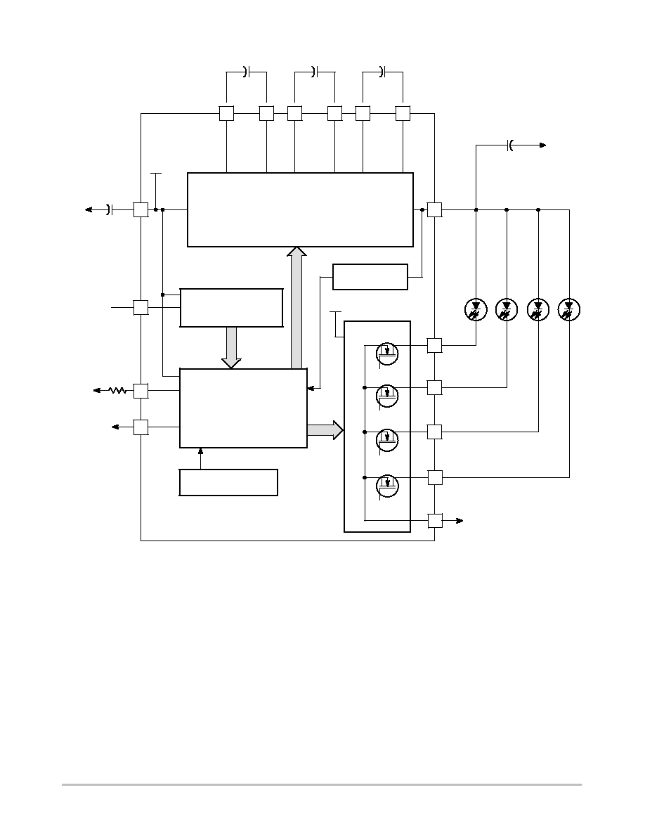
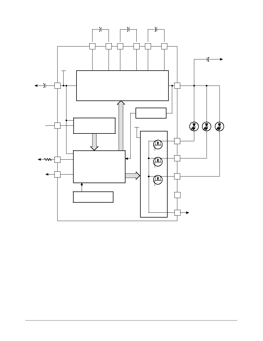
The NCP5604A and NCP5604B products are multiple output LED
drivers dedicated to the display back light. The NCP5604A drives up
to 4 LEDs, the NCP5604B version being dedicated to the three LED
applications.
The two parts share a common built-in DC/DC converter, based on
a charge pump structure, including the new 1.33X mode of operation,
improving the efficiency over the full input battery supply voltage
span over 90%.
Features
∑
2.7 to 5.5 V Input Voltage Range
∑
Consistent 85% Efficiency
∑
1.0
mA Quiescent Supply Current
∑
All Pins are Fully ESD Protected
∑
Built-in Short Circuit Protection
∑
Provides Four Independent LED Drives
∑
200 kHz Digital Dimming Function
∑
Unloaded LED Protection
∑
Short Circuit Current Proof
∑
Tight 0.5% LED Current Matching
∑
These are Pb-Free Devices
Typical Applications
∑
Portable Back Light
∑
Digital Cellular Phone Camera Photo Flash
∑
LCD and Key Board Simultaneously Drive
*For additional information on our Pb-Free strategy and soldering details, please
download the ON Semiconductor Soldering and Mounting Techniques Reference
Manual, SOLDERRM/D.
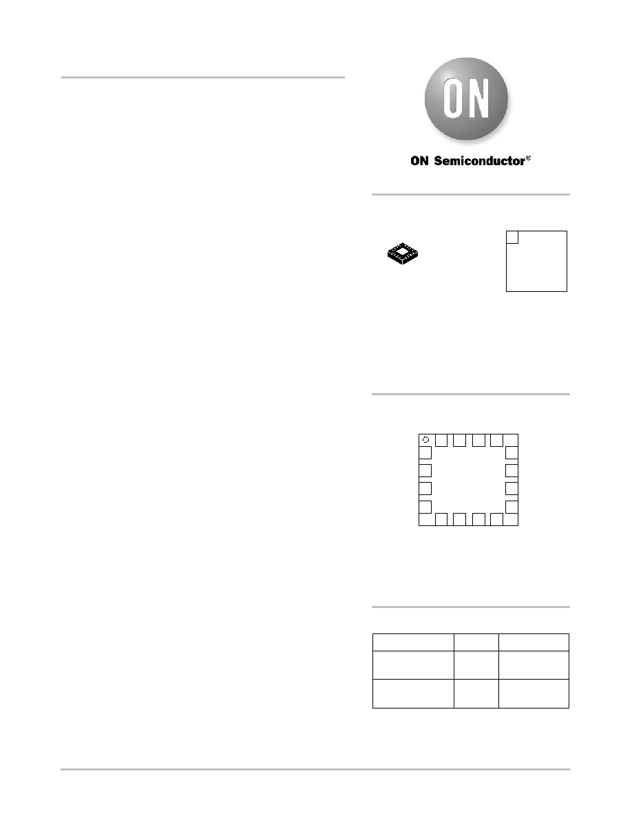
WQFN16 (3x3)
MT SUFFIX
CASE 488AK
Device
Package
Shipping
ORDERING INFORMATION
NCP5604AMTR2G
WQFN16
(Pb-Free)
3000/Tape & Reel
MARKING
DIAGRAM
NCPx5604 = Specific Device Code
x = A or B
A
= Assembly Location
L
= Wafer Lot
Y
= Year
W
= Work Week
G
= Pb-Free Package
http://onsemi.com
1
16
NCPx
5604
ALYW
G
G
1
««
««
AGND
PGND
9
10
11
12
4
3
2
1
5
6
7
8
16
15
14
13
I
REF
C1N
EN
C1P
V
bat
V
OUT
C3N
C3P
C2N
C2P
LED4/NC*
LED3
LED2
LED1
PIN CONNECTIONS
(Top View)
NCP5604BMTR2G
WQFN16
(Pb-Free)
3000/Tape & Reel
* Pin 5 in not connected in the NCP5604B
For information on tape and reel specifications,
including part orientation and tape sizes, please
refer to our Tape and Reel Packaging Specification
Brochure, BRD8011/D.
(Note: Microdot may be in either location)

NCP5604A, NCP5604B
http://onsemi.com
5
PIN FUNCTION DESCRIPTION
Pin
Symbol
Type
Description
1
VBAT
INPUT, POWER
Input Battery voltage to supply the analog and digital blocks. The pin must be decoupled to
ground by a 1.0
m
F ceramic capacitor.
2
EN
INPUT, DIGITAL
This pin carries the Enable function to control the DC-DC converter. It can be used to
digitally dim the LED by using a PWM technique.
EN = Low
≥
shutdown mode, the DC-DC is disconnected from the load.
EN = High
≥
operating mode, the DC-DC is activated.
The digital PWM dimming can operate over the 100 Hz - 200 kHz frequency, depending
upon the application requirements.
3
I
REF
INPUT, ANALOG
This pin provides the reference current, based on the internal bandgap voltage reference,
to control the output current flowing in the LED. A 1% tolerance, or better, resistor shall be
used to get the highest accuracy of the LED biases. An external current source can be
used to bias this pin to dim the light coming out of the LED.
In no case shall the voltage at pin 3 be forced either higher or lower than the 600 mV
provided by the internal reference.
4
AGND
POWER
This pin is the GROUND signal for the analog and digital blocks and must be connected to
the system ground.
5
LED4
INPUT, POWER
NCP5604A: This pin sinks to ground and monitors the current flowing into the fourth LED,
intended to be used in backlight application. The current is limited to 25 mA maximum
(Note 2).
NCP5604B: This pin is not connected.
6
LED3
INPUT, POWER
This pin sinks to ground and monitors the current flowing into the third LED, intended to be
used in backlight application. The current is limited to 25 mA maximum (Note 2).
7
LED2
INPUT, POWER
This pin sinks to ground and monitors the current flowing into the second LED, intended to
be used in backlight application. The current is limited to 25mA maximum (Note 2).
8
LED1
INPUT, POWER
This pin sinks to ground and monitors the current flowing into the first LED, intended to be
used in backlight application. The current is limited to 25 mA maximum (Note 2).
9
PGND
POWER
This pin is the GROUND reference for the DC-DC converter and the output current
control. The pin must be connected to the system ground, a ground plane being strongly
recommended.
10
C1P
POWER
One side of the external charge pump capacitor (C
FLY
) is connected to this pin, associated
with C1N, pin 11 (Note 1).
11
C1N
POWER
One side of the external charge pump capacitor (C
FLY
) is connected to this pin, associated
with C1P, pin 10 (Note 1).
12
VOUT
OUTPUT, POWER
This pin provides the output voltage supplied by the DC-DC converter. The Vout pin must
be bypassed by 1.0
m
F ceramic capacitor located as close as possible to the pin to
properly bypass the output voltage to ground. The circuit shall not operate without such
bypass capacitor properly connected to the Vout pin.
The output voltage is internally clamped to 5.5 V in the event of no load situation. On the
other hand, the output current is limited to 100 mA in the event of a short circuit to ground.
13
C2P
POWER
One side of the external charge pump capacitor (C
FLY
) is connected to this pin, associated
with C2N, pin 14 (Note 1).
14
C2N
POWER
One side of the external charge pump capacitor (C
FLY
) is connected to this pin, associated
with C2P, pin 13 (Note 1).
15
C3P
POWER
One side of the external charge pump capacitor (C
FLY
) is connected to this pin, associated
with C3N, pin 16 (Note 1).
16
C3N
POWER
One side of the external charge pump capacitor (C
FLY
) is connected to this pin, associated
with C3P, pin 15 (Note 1).
1. Using low ESR 1.0
m
F ceramic capacitor is mandatory to optimize the Charge Pump efficiency. The DC Bias effect must be taken into account
when selecting the ceramic capacitor. Smallest foot print packages (size 0602 and lower) are prone to strong DC bias effect, reducing the real
capacitance significantly.
2. Total DC-DC output current is limited to 100 mA.
3. The exposed flag shall be connected to ground.