©
Semiconductor Components Industries, LLC, 2004
January, 2004 - Rev. 6
1
Publication Order Number:
NCP562/D
NCP562, NCP563
80 mA CMOS Low Iq
Low-Dropout Voltage
Regulator
This series of fixed output low-dropout linear regulators are
designed for handheld communication equipment and portable battery
powered applications which require low quiescent. This series
features an ultra-low quiescent current of 2.5
mA. Each device
contains a voltage reference unit, an error amplifier, a PMOS power
transistor, resistors for setting output voltage, current limit, and
temperature limit protection circuits. The NCP562 series provides an
enable pin for ON/OFF control.
The NCP562 has been designed to be used with low cost ceramic
capacitors and requires a minimum output capacitor of 0.1
mF. The
device is housed in the micro-miniature SC82-AB surface mount
package. Standard voltage versions are 1.5, 1.8, 2.5, 2.7, 2.8, 3.0, 3.3,
and 5.0 V. Other voltages are available in 100 mV steps.
Features
∑
Low Quiescent Current of 2.5
mA Typical
∑
Low Output Voltage Option
∑
Output Voltage Accuracy of 2.0%
∑
Temperature Range of -40
∞
C to 85
∞
C
∑
NCP562 Provides an Enable Pin
∑
Pb-Free Package May be Available.* The G-Suffix Denotes a
Pb-Free Lead Finish
Typical Applications
∑
Battery Powered Instruments
∑
Hand-Held Instruments
∑
Camcorders and Cameras
Figure 1. NCP562 Typical Application Diagram
This device contains 28 active transistors
Output
C2
+
Input
GND Enable
V
in
V
out
+
C1
OFF
ON
Figure 2. NCP563 Typical Application Diagram
This device contains 28 active transistors
Output
C2
+
Input
GND
N/C
V
in
V
out
+
C1
See detailed ordering and shipping information in the package
dimensions section on page 8 of this data sheet.
ORDERING INFORMATION
SC82-AB (SC70-4)
SQ SUFFIX
CASE 419C
1
4
PIN CONNECTIONS &
MARKING DIAGRAMS
GND
(NCP562 Top View)
1
2
4
3
V
in
Enable
V
out
xxxM
xxx
= Device Code
M
= Date Code
GND 1
2
4
3
V
in
N/C
V
out
xxxM
(NCP563 Top View)
http://onsemi.com
*For additional information on our Pb-Free strategy
and soldering details, please download the
ON Semiconductor Soldering and Mounting Tech-
niques Reference Manual, SOLDERRM/D.
NCP562, NCP563
http://onsemi.com
2
¡¡¡¡¡¡¡¡¡¡¡¡¡¡¡¡¡¡¡¡¡¡¡¡¡¡¡¡¡¡¡¡¡
¡¡¡¡¡¡¡¡¡¡¡¡¡¡¡¡¡¡¡¡¡¡¡¡¡¡¡¡¡¡¡¡¡
PIN FUNCTION DESCRIPTION
¡¡¡¡
¡¡¡¡
NCP562
¡¡¡
¡¡¡
NCP563
¡¡¡¡¡
¡¡¡¡¡
Pin Name
¡¡¡¡¡¡¡¡¡¡¡¡¡¡¡¡¡¡¡¡¡¡¡¡
¡¡¡¡¡¡¡¡¡¡¡¡¡¡¡¡¡¡¡¡¡¡¡¡
Description
¡¡¡¡
¡¡¡¡
1
¡¡¡
¡¡¡
1
¡¡¡¡¡
¡¡¡¡¡
GND
¡¡¡¡¡¡¡¡¡¡¡¡¡¡¡¡¡¡¡¡¡¡¡¡
¡¡¡¡¡¡¡¡¡¡¡¡¡¡¡¡¡¡¡¡¡¡¡¡
Power supply ground.
¡¡¡¡
¡¡¡¡
2
¡¡¡
¡¡¡
2
¡¡¡¡¡
¡¡¡¡¡
Vin
¡¡¡¡¡¡¡¡¡¡¡¡¡¡¡¡¡¡¡¡¡¡¡¡
¡¡¡¡¡¡¡¡¡¡¡¡¡¡¡¡¡¡¡¡¡¡¡¡
Positive power supply input voltage.
¡¡¡¡
¡¡¡¡
3
¡¡¡
¡¡¡
3
¡¡¡¡¡
¡¡¡¡¡
Vout
¡¡¡¡¡¡¡¡¡¡¡¡¡¡¡¡¡¡¡¡¡¡¡¡
¡¡¡¡¡¡¡¡¡¡¡¡¡¡¡¡¡¡¡¡¡¡¡¡
Regulated output voltage.
¡¡¡¡
¡
¡¡
¡
¡¡¡¡
4
¡¡¡
¡
¡
¡
¡¡¡
-
¡¡¡¡¡
¡
¡¡¡
¡
¡¡¡¡¡
Enable
¡¡¡¡¡¡¡¡¡¡¡¡¡¡¡¡¡¡¡¡¡¡¡¡
¡
¡¡¡¡¡¡¡¡¡¡¡¡¡¡¡¡¡¡¡¡¡¡
¡
¡¡¡¡¡¡¡¡¡¡¡¡¡¡¡¡¡¡¡¡¡¡¡¡
This input is used to place the device into low-power standby. When this input is pulled low, the de-
vice is disabled. If this function is not used, Enable should be connected to Vin.
¡¡¡¡
¡¡¡¡
-
¡¡¡
¡¡¡
4
¡¡¡¡¡
¡¡¡¡¡
N/C
¡¡¡¡¡¡¡¡¡¡¡¡¡¡¡¡¡¡¡¡¡¡¡¡
¡¡¡¡¡¡¡¡¡¡¡¡¡¡¡¡¡¡¡¡¡¡¡¡
No internal connection.
MAXIMUM RATINGS
Rating
Symbol
Value
Unit
¡¡¡¡¡¡¡¡¡¡¡¡¡¡¡¡¡¡
¡¡¡¡¡¡¡¡¡¡¡¡¡¡¡¡¡¡
Input Voltage
¡¡¡¡¡¡
¡¡¡¡¡¡
V
in
¡¡¡¡¡¡¡¡
¡¡¡¡¡¡¡¡
6.0
¡¡¡¡
¡¡¡¡
V
¡¡¡¡¡¡¡¡¡¡¡¡¡¡¡¡¡¡
¡¡¡¡¡¡¡¡¡¡¡¡¡¡¡¡¡¡
Enable Voltage (NCP562 ONLY)
¡¡¡¡¡¡
¡¡¡¡¡¡
Enable
¡¡¡¡¡¡¡¡
¡¡¡¡¡¡¡¡
-0.3 to V
in
+0.3
¡¡¡¡
¡¡¡¡
V
¡¡¡¡¡¡¡¡¡¡¡¡¡¡¡¡¡¡
¡¡¡¡¡¡¡¡¡¡¡¡¡¡¡¡¡¡
Output Voltage
¡¡¡¡¡¡
¡¡¡¡¡¡
V
out
¡¡¡¡¡¡¡¡
¡¡¡¡¡¡¡¡
-0.3 to V
in
+0.3
¡¡¡¡
¡¡¡¡
V
¡¡¡¡¡¡¡¡¡¡¡¡¡¡¡¡¡¡
¡
¡¡¡¡¡¡¡¡¡¡¡¡¡¡¡¡¡
¡
¡¡¡¡¡¡¡¡¡¡¡¡¡¡¡¡¡
¡¡¡¡¡¡¡¡¡¡¡¡¡¡¡¡¡¡
Power Dissipation and Thermal Characteristics
Power Dissipation
Thermal Resistance, Junction to Ambient
¡¡¡¡¡¡
¡
¡¡¡¡
¡
¡
¡¡¡¡
¡
¡¡¡¡¡¡
P
D
R
q
JA
¡¡¡¡¡¡¡¡
¡
¡¡¡¡¡¡
¡
¡
¡¡¡¡¡¡
¡
¡¡¡¡¡¡¡¡
Internally Limited
400
¡¡¡¡
¡
¡¡
¡
¡
¡¡
¡
¡¡¡¡
W
∞
C/W
Operating Junction Temperature
T
J
+125
∞
C
¡¡¡¡¡¡¡¡¡¡¡¡¡¡¡¡¡¡
¡¡¡¡¡¡¡¡¡¡¡¡¡¡¡¡¡¡
Operating Ambient Temperature
¡¡¡¡¡¡
¡¡¡¡¡¡
T
A
¡¡¡¡¡¡¡¡
¡¡¡¡¡¡¡¡
-40 to +85
¡¡¡¡
¡¡¡¡
∞
C
¡¡¡¡¡¡¡¡¡¡¡¡¡¡¡¡¡¡
¡¡¡¡¡¡¡¡¡¡¡¡¡¡¡¡¡¡
Storage Temperature
¡¡¡¡¡¡
¡¡¡¡¡¡
T
stg
¡¡¡¡¡¡¡¡
¡¡¡¡¡¡¡¡
-55 to +150
¡¡¡¡
¡¡¡¡
∞
C
1. This device series contains ESD protection and exceeds the following tests:
Human Body Model 2000 V per MIL-STD-883, Method 3015
Machine Model Method 200 V
2. Latch up capability (85
∞
C)
"
100 mA DC with trigger voltage.
NCP562, NCP563
http://onsemi.com
3
ELECTRICAL CHARACTERISTICS
(V
in
= V
out(nom.)
+ 1.0 V, V
enable
= V
in
, C
in
= 1.0
m
F, C
out
= 1.0
m
F, T
J
= 25
∞
C, unless otherwise noted.)
Characteristic
Symbol
Min
Typ
Max
Unit
Output Voltage (T
A
= 25
∞
C, I
out
= 1.0 mA)
1.5 V
1.8 V
2.5 V
2.7 V
2.8 V
3.0 V
3.3 V
5.0 V
V
out
1.455
1.746
2.425
2.646
2.744
2.940
3.234
4.9
1.5
1.8
2.5
2.7
2.8
3.0
3.3
5.0
1.545
1.854
2.575
2.754
2.856
3.060
3.366
5.1
V
Line Regulation
1.5 V-4.4 V (V
in
= V
o(nom.)
+ 1.0 V to 6.0 V
4.5 V-5.0 V (V
in
= 5.5 V to 6.0 V)
Reg
line
-
-
10
10
20
20
mV
Load Regulation (I
out
= 10 mA to 80 mA)
Reg
load
-
20
40
mV
Output Current (V
out
= (V
out
at I
out
= 80 mA) -3.0%)
1.5 V to 3.9 V (V
in
= V
out(nom.)
+ 2.0 V)
4.0 V-5.0 V (V
in
= 6.0 V)
I
o(nom.)
80
80
280
280
-
-
mA
Dropout Voltage (T
A
= -40
∞
C to 85
∞
C, I
out
= 80 mA, Measured at
V
out
-3.0%)
1.5 V-1.7 V
1.8 V-2.4 V
2.5 V-2.6 V
2.7 V-2.9 V
3.0 V-3.2 V
3.3 V-4.9 V
5.0 V
V
in
-V
out
-
-
-
-
-
-
-
550
400
250
230
200
190
140
800
550
400
400
350
350
250
mV
Quiescent Current
(Enable Input = 0 V)
(Enable Input = V
in
, I
out
= 1.0 mA to I
o(nom.)
)
I
Q
-
-
0.1
2.5
1.0
6.0
m
A
Output Short Circuit Current
1.5 V to 3.9 V (V
in
= V
nom
+ 2.0 V)
4.0 V-5.0 V (V
in
= 6.0 V)
I
out(max)
150
150
300
300
600
600
mA
Output Voltage Noise (f = 100 Hz to 100 kHz, V
out
= 3.0 V)
V
n
-
100
-
m
Vrms
Enable Input Threshold Voltage (NCP562 ONLY)
(Voltage Increasing, Output Turns On, Logic High)
(Voltage Decreasing, Output Turns Off, Logic Low)
V
th(en)
1.3
-
-
-
-
0.3
V
Output Voltage Temperature Coefficient
T
C
-
"
100
-
ppm/
∞
C
3. Maximum package power dissipation limits must be observed.
PD
+
TJ(max)
*
TA
R
q
JA
4. Low duty cycle pulse techniques are used during testing to maintain the junction temperature as close to ambient as possible.
NCP562, NCP563
http://onsemi.com
4
0
0
V
IN
, INPUT VOLTAGE (V)
I
Q
, QUIESCENT CURRENT (
m
A)
I
Q
, QUIESCENT CURRENT (
m
A)
100
20
0
-20
-40
-60
1.7
2.9
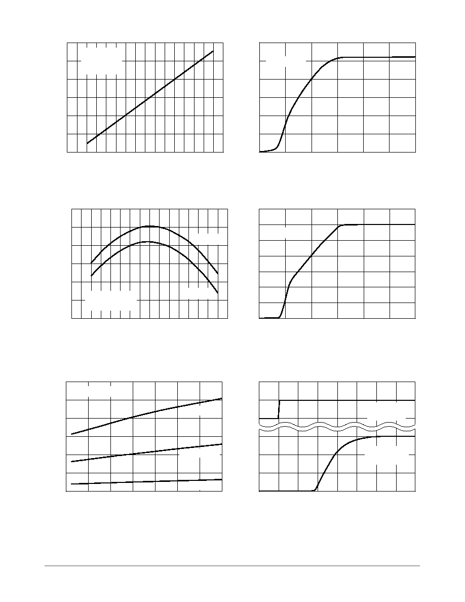
Figure 3. Quiescent Current versus Temperature
T, TEMPERATURE (
∞
C)
Figure 4. Quiescent Current versus Input
Voltage
Figure 5. Output Voltage versus Temperature
Figure 6. Output Voltage versus Input Voltage
Figure 7. Dropout Voltage versus Temperature
Figure 8. Turn-On Response (NCP562 ONLY)
2.7
2.5
6
5
3
2
1
0
0
3
2
1
0.5
V
IN
- V
OUT
, DROPOUT VOL
T
AGE (mV)
125
25
-50
T, TEMPERATURE (
∞
C)
300
4
V
OUT
, OUTPUT
VOL
T
AGE (V)
400
250
200
100
50
0
t, TIME (
m
s)
1
1.9
2.5
V
OUT
, OUTPUT VOL
T
AGE (V)
100
60
40
20
-20
-40
-60
T, TEMPERATURE (
∞
C)
V
OUT
, OUTPUT VOL
T
AGE (V)
6
1
0
0
3.5
V
IN
, INPUT VOLTAGE (V)
3
2.5
2.990
3.020
3.000
2.1
2.3
V
IN
= 4.0 V
V
OUT
= 3.0 V
I
OUT
= 0 mA
1.5
V
OUT
= 3.0 V
0
80
2.995
3.015
3.005
3.010
V
IN
= 6.0 V
I
OUT
= 30 mA
V
OUT(nom)
= 3.0 V
80 mA LOAD
V
IN
= 4.0 V
C
IN
= 1.0
m
F
3
2
2
0
150
40
60
80
4
V
IN
= 4.0 V
V
OUT(nom)
= 3.0 V
I
OUT
= 10 mA
2
3
4
5
2
1.5
1
0.5
-25
0
50
75
100
250
200
150
100
50
40 mA LOAD
10 mA LOAD
300
350
C
OUT
= 0.1
m
F
I
OUT
= 10 mA
ENABLE
VOL
T
AGE (V)

NCP562, NCP563
http://onsemi.com
5
-400
0
Figure 9. Line Transient Response
Figure 10. Load Transient Response
3.5
V
n
, OUTPUT VOL
T
AGE NOISE (mV/
Hz
)
1000
1
0.1
0.01
f, FREQUENCY (kHz)
0.5
V
IN
= 5.0 V
V
OUT
= 3.0 V
I
OUT
= 50 mA
C
OUT
= 0.1
m
F
1.5
1
2
2.5
10
100
-1
6
OUTPUT VOL
T
AGE
DEVIA
TION (V)
500
250
200
100
50
0
t, TIME (
m
s)
-0.5
1
0
4
3
150
300
350
V
OUT
= 3.0 V
C
OUT
= 0.1
m
F
I
OUT
= 10 mA
V
IN
, INPUT
VOL
T
AGE (V)
400
450
0.5
5
60
OUTPUT VOL
T
AGE
DEVIA
TION (mV)
500
250
200
100
50
0
t, TIME (
m
s)
-1
0.5
-0.5
0
-30
150
300
350
I
OUT
, OUTPUT
CURRENT (mA)
400
450
0
30
1
3
I
OUT
= 1 mA to 30
mA
V
IN
= 4.0 V
V
OUT
= 3.0 V
C
OUT
= 0.1
m
F
60
600
200
100
500
0
t, TIME (
m
s)
-30
0
0
400
300
700
400
800
-200
30
200
I
OUT
= 1 mA to 30
mA
V
IN
= 4.0 V
C
OUT
= 1.0
m
F
V
OUT
= 3.0 V
OUTPUT VOL
T
AGE
DEVIA
TION (mV)
I
OUT
, OUTPUT
CURRENT (mA)
900 1000
Figure 11. Load Transient Response
Figure 12. Output Voltage Noise

NCP562, NCP563
http://onsemi.com
6
DEFINITIONS
Load Regulation
The change in output voltage for a change in output
current at a constant temperature.
Dropout Voltage
The input/output differential at which the regulator output
no longer maintains regulation against further reductions in
input voltage. Measured when the output drops 3.0% below
its nominal. The junction temperature, load current, and
minimum input supply requirements affect the dropout level.
Maximum Power Dissipation
The maximum total dissipation for which the regulator
will operate within its specifications.
Quiescent Current
The quiescent current is the current which flows through
the ground when the LDO operates without a load on its
output: internal IC operation, bias, etc. When the LDO
becomes loaded, this term is called the Ground current. It is
actually the difference between the input current (measured
through the LDO input pin) and the output current.
Line Regulation
The change in output voltage for a change in input voltage.
The measurement is made under conditions of low
dissipation or by using pulse technique such that the average
chip temperature is not significantly affected.
Line Transient Response
Typical over and undershoot response when input voltage
is excited with a given slope.
Thermal Protection
Internal thermal shutdown circuitry is provided to protect
the integrated circuit in the event that the maximum junction
temperature is exceeded. When activated at typically 160
∞
C,
the regulator turns off. This feature is provided to prevent
failures from accidental overheating.
Maximum Package Power Dissipation
The maximum power package dissipation is the power
dissipation level at which the junction temperature reaches
its maximum operating value, i.e. 125
∞
C. Depending on the
ambient power dissipation and thus the maximum available
output current.

NCP562, NCP563
http://onsemi.com
7
APPLICATIONS INFORMATION
A typical application circuit for the NCP562 and NCP563
series are shown in Figure 1 and Figure 2.
Input Decoupling (C1)
A 1.0
mF capacitor either ceramic or tantalum is
recommended
and should be connected close to the NCP562
package. Higher values and lower ESR will improve the
overall line transient response.
TDK capacitor: C2012X5R1C105K, or C1608X5R1A105K
Output Decoupling (C2)
The NCP562 and NCP563 are very stable regulators and
do not require any specific Equivalent Series Resistance
(ESR) or a minimum output current. Capacitors exhibiting
ESRs ranging from a few m
W up to 10 W can thus safely be
used. The minimum decoupling value is 0.1
mF and can be
augmented to fulfill stringent load transient requirements.
The regulator accepts ceramic chip capacitors as well as
tantalum devices. Larger values improve noise rejection and
load regulation transient response.
TDK capacitor: C2012X5R1C105K, C1608X5R1A105K,
or C3216X7R1C105K
Enable Operation (NCP562 ONLY)
The enable pin will turn on the regulator when pulled high
and turn off the regulator when pulled low. These limits of
threshold are covered in the electrical specification section
of this data sheet. If the enable is not used, then the pin
should be connected to V
in
.
Hints
Please be sure the Vin and GND lines are sufficiently
wide. When the impedance of these lines is high, there is a
chance to pick up noise or cause the regulator to
malfunction.
Place external components, especially the output
capacitor, as close as possible to the circuit, and make leads
as short as possible.
Thermal
As power across the NCP562 and NCP563 increases, it
might become necessary to provide some thermal relief. The
maximum power dissipation supported by the device is
dependent upon board design and layout. Mounting pad
configuration on the PCB, the board material and also the
ambient temperature effect the rate of temperature rise for
the part. This is stating that when the devices have good
thermal conductivity through the PCB, the junction
temperature will be relatively low with high power
dissipation applications.
The maximum dissipation the package can handle is
given by:
PD
+
TJ(max)
*
TA
R
q
JA
If junction temperature is not allowed above the
maximum 125
∞
C, then the NCP562 and NCP563 can
dissipate up to 250 mW @ 25
∞
C.
The power dissipated by the NCP562 and NCP563 can be
calculated from the following equation:
Ptot
+
[Vin * Ignd (Iout)]
)
[Vin
*
Vout] * Iout
or
VinMAX
+
Ptot
)
Vout * Iout
Ignd
)
Iout
If an 80 mA output current is needed then the ground
current from the data sheet is 2.5
mA. For an NCP562 or
NCP563 (3.0 V), the maximum input voltage will then be
6.0 V.

NCP562, NCP563
http://onsemi.com
8
ORDERING INFORMATION
Device
Nominal
Output Voltage
Marking
Package
Shipping
NCP562SQ15T1
1.5
LDI
NCP562SQ15T1G
1.5
LDI
NCP562SQ18T1
1.8
LEY
NCP562SQ18T1G
1.8
LEY
NCP562SQ25T1
2.5
LDK
NCP562SQ25T1G
2.5
LDK
NCP562SQ27T1
2.7
LEZ
NCP562SQ27T1G
2.7
LEZ
SC82 AB
3000 Units/
NCP562SQ28T1
2.8
LDL
SC82-AB
3000 Units/
8
Tape & Reel
NCP562SQ28T1G
2.8
LDL
NCP562SQ30T1
3.0
LDM
NCP562SQ30T1G
3.0
LDM
NCP562SQ33T1
3.3
LDN
NCP562SQ33T1G
3.3
LDN
NCP562SQ50T1
5.0
LDP
NCP562SQ50T1G
5.0
LDP
NCP563SQ15T1
1.5
LDQ
NCP563SQ15T1G
1.5
LDQ
NCP563SQ18T1
1.8
LFA
NCP563SQ18T1G
1.8
LFA
NCP563SQ25T1
2.5
LDS
NCP563SQ25T1G
2.5
LDS
NCP563SQ27T1
2.7
LFB
NCP563SQ27T1G
2.7
LFB
SC82-AB
3000 Units/
NCP563SQ28T1
2.8
LDT
SC82-AB
3000 Units/
8
Tape & Reel
NCP563SQ28T1G
2.8
LDT
NCP563SQ30T1
3.0
LDU
NCP563SQ30T1G
3.0
LDU
NCP563SQ33T1
3.3
LDV
NCP563SQ33T1G
3.3
LDV
NCP563SQ50T1
5.0
LDX
NCP563SQ50T1G
5.0
LDX
For information on tape and reel specifications, including part orientation and tape sizes, please refer to our Tape and Reel Packaging
Specifications Brochure, BRD8011/D.
NCP562, NCP563
http://onsemi.com
9
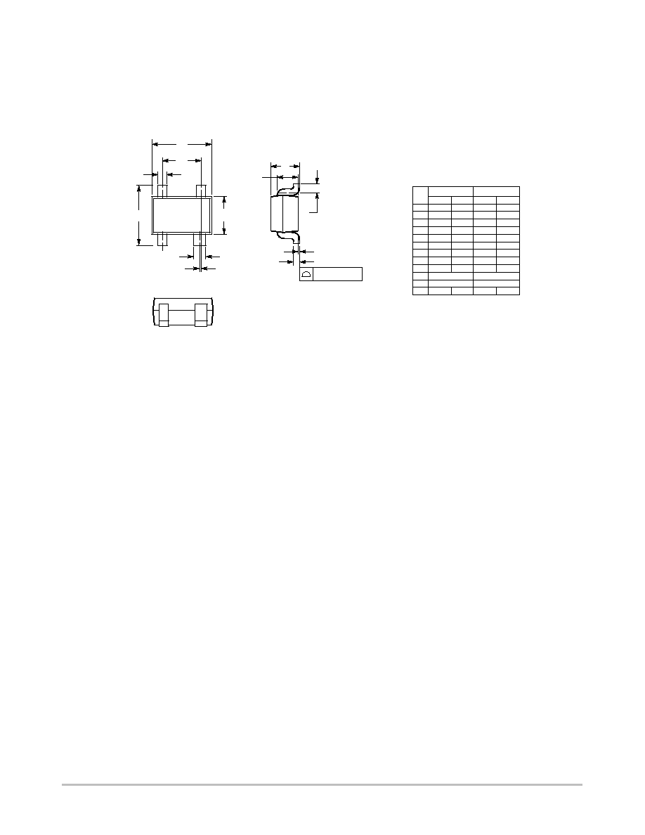
PACKAGE DIMENSIONS
SC82-AB (SC70-4)
SQ SUFFIX
CASE 419C-02
ISSUE C
NOTES:
1. DIMENSIONING AND TOLERANCING PER
ANSI Y14.5M, 1982.
2. CONTROLLING DIMENSION: MILLIMETER.
3. 419C-01 OBSOLETE. NEW STANDARD IS
419C-02.
4. DIMENSIONS A AND B DO NOT INCLUDE
MOLD FLASH, PROTRUSIONS, OR GATE
BURRS.
1
2
3
A
G
S
N
J
K
4
D
3 PL
B
F
L
C
H
0.05 (0.002)
DIM
MIN
MAX
MIN
MAX
INCHES
MILLIMETERS
A
1.8
2.2
0.071
0.087
B
1.15
1.35
0.045
0.053
C
0.8
1.1
0.031
0.043
D
0.2
0.4
0.008
0.016
F
0.3
0.5
0.012
0.020
G
1.1
1.5
0.043
0.059
H
0.0
0.1
0.000
0.004
J
0.10
0.26
0.004
0.010
K
0.1
---
0.004
---
L
0.05 BSC
0.002 BSC
N
0.2 REF
0.008 REF
S
1.8
2.4
0.07
0.09

NCP562, NCP563
http://onsemi.com
10
ON Semiconductor and are registered trademarks of Semiconductor Components Industries, LLC (SCILLC). SCILLC reserves the right to make changes without further notice
to any products herein. SCILLC makes no warranty, representation or guarantee regarding the suitability of its products for any particular purpose, nor does SCILLC assume any liability
arising out of the application or use of any product or circuit, and specifically disclaims any and all liability, including without limitation special, consequential or incidental damages.
"Typical" parameters which may be provided in SCILLC data sheets and/or specifications can and do vary in different applications and actual performance may vary over time. All
operating parameters, including "Typicals" must be validated for each customer application by customer's technical experts. SCILLC does not convey any license under its patent rights
nor the rights of others. SCILLC products are not designed, intended, or authorized for use as components in systems intended for surgical implant into the body, or other applications
intended to support or sustain life, or for any other application in which the failure of the SCILLC product could create a situation where personal injury or death may occur. Should
Buyer purchase or use SCILLC products for any such unintended or unauthorized application, Buyer shall indemnify and hold SCILLC and its officers, employees, subsidiaries, affiliates,
and distributors harmless against all claims, costs, damages, and expenses, and reasonable attorney fees arising out of, directly or indirectly, any claim of personal injury or death
associated with such unintended or unauthorized use, even if such claim alleges that SCILLC was negligent regarding the design or manufacture of the part. SCILLC is an Equal
Opportunity/Affirmative Action Employer. This literature is subject to all applicable copyright laws and is not for resale in any manner.
PUBLICATION ORDERING INFORMATION
N. American Technical Support: 800-282-9855 Toll Free
USA/Canada
Japan: ON Semiconductor, Japan Customer Focus Center
2-9-1 Kamimeguro, Meguro-ku, Tokyo, Japan 153-0051
Phone: 81-3-5773-3850
NCP562/D
LITERATURE FULFILLMENT:
Literature Distribution Center for ON Semiconductor
P.O. Box 5163, Denver, Colorado 80217 USA
Phone: 303-675-2175 or 800-344-3860 Toll Free USA/Canada
Fax: 303-675-2176 or 800-344-3867 Toll Free USA/Canada
Email: orderlit@onsemi.com
ON Semiconductor Website: http://onsemi.com
Order Literature: http://www.onsemi.com/litorder
For additional information, please contact your
local Sales Representative.