©
Semiconductor Components Industries, LLC, 2005
August, 2005 - Rev. 2
1
Publication Order Number:
NCP580/D
NCP580
Ultra-Fast, Low Noise
120 mA CMOS LDO
Regulator with Enable
The NCP580 series of low dropout regulators are designed for
portable battery powered applications which require precise output
voltage accuracy, low quiescent current, and high ripple rejection.
These devices feature an enable function which lowers current
consumption significantly and are offered in the small SC-82AB
package.
A 2.2
mF ceramic capacitor or higher is the recommended value to
be used with these devices on the output pin.
Features
∑
Ultra-Low Dropout Voltage of 150 mV at 100 mA
∑
Low Output Noise of 30
mVrms without Noise Reduction Cap
∑
Excellent Line Regulation of 0.02%/V
∑
Excellent Load Regulation of 12 mV
∑
High Output Voltage Accuracy of
"1.5%
∑
Low Iq Current of 90
mA
∑
Very Low Shutdown Current of 0.1
mA
∑
Excellent Power Supply Rejection Ratio of 70 dB at f = 1.0 kHz
∑
Wide Output Voltage Range of 1.5 V to 3.3 V
∑
Fold Back Protection Circuit
∑
Fast Dynamic Performance
∑
Low Temperature Drift Coefficient on the Output Voltage of
"100 ppm/∞C
∑
Input Voltage up to 6.5 V
∑
These are Pb-Free Devices
Typical Applications
∑
Portable Equipment
∑
Hand-Held Instrumentation
∑
Camcorders and Cameras
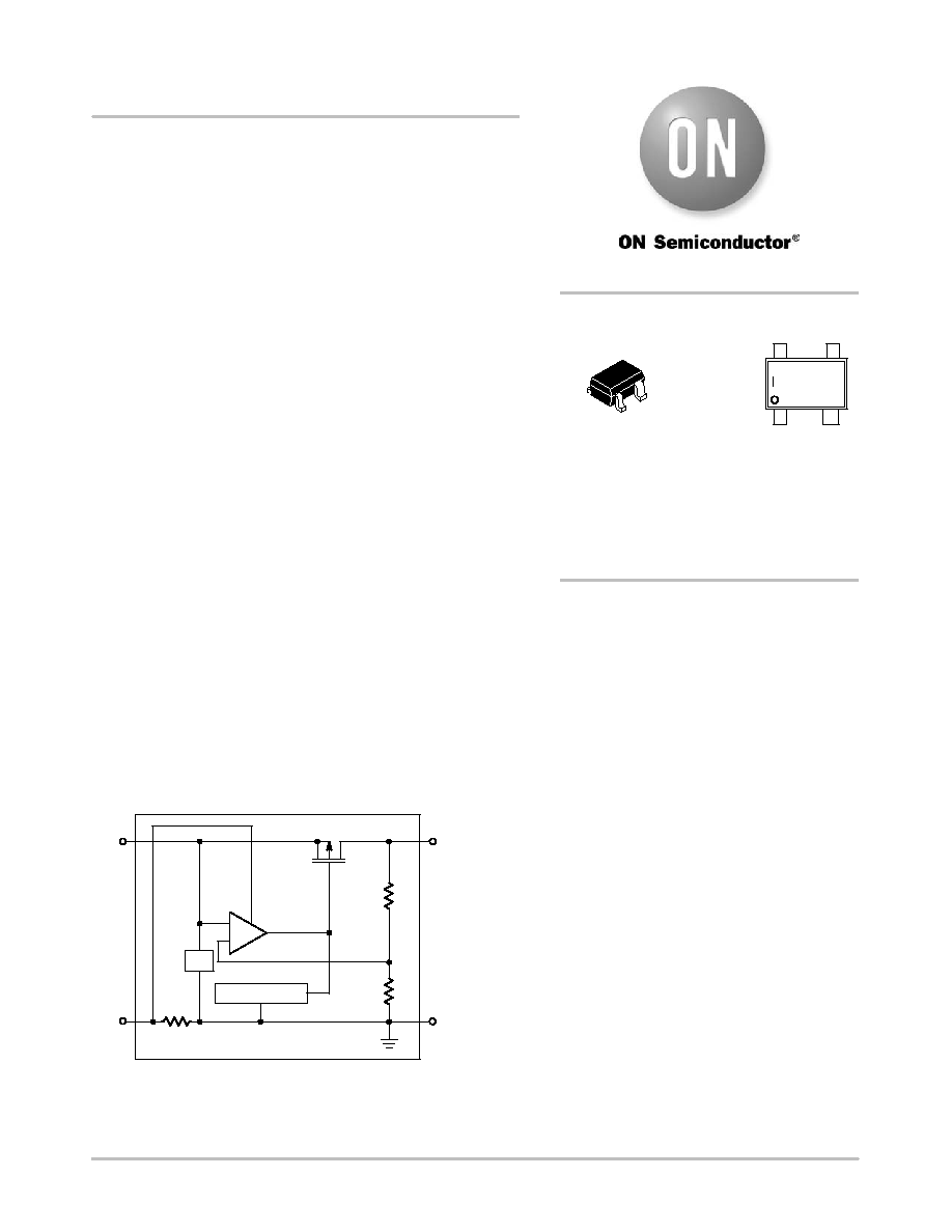
Figure 1. Simplified Block Diagram
+
-
V
in
V
ref
Current Limit
CE
V
out
GND
SC-82AB
SQ SUFFIX
CASE 419C
http://onsemi.com
MARKING
DIAGRAM
1
4
See detailed ordering and shipping information in the package
dimensions section on page 8 of this data sheet.
ORDERING INFORMATION
xxx M
G
1
M
G
xxx = Device Code
M
= Date Code*
G
= Pb-Free Package
(Note: Microdot may be in either location)
*Date Code orientation and/or position may
vary depending upon manufacturing location.
NCP580
http://onsemi.com
2
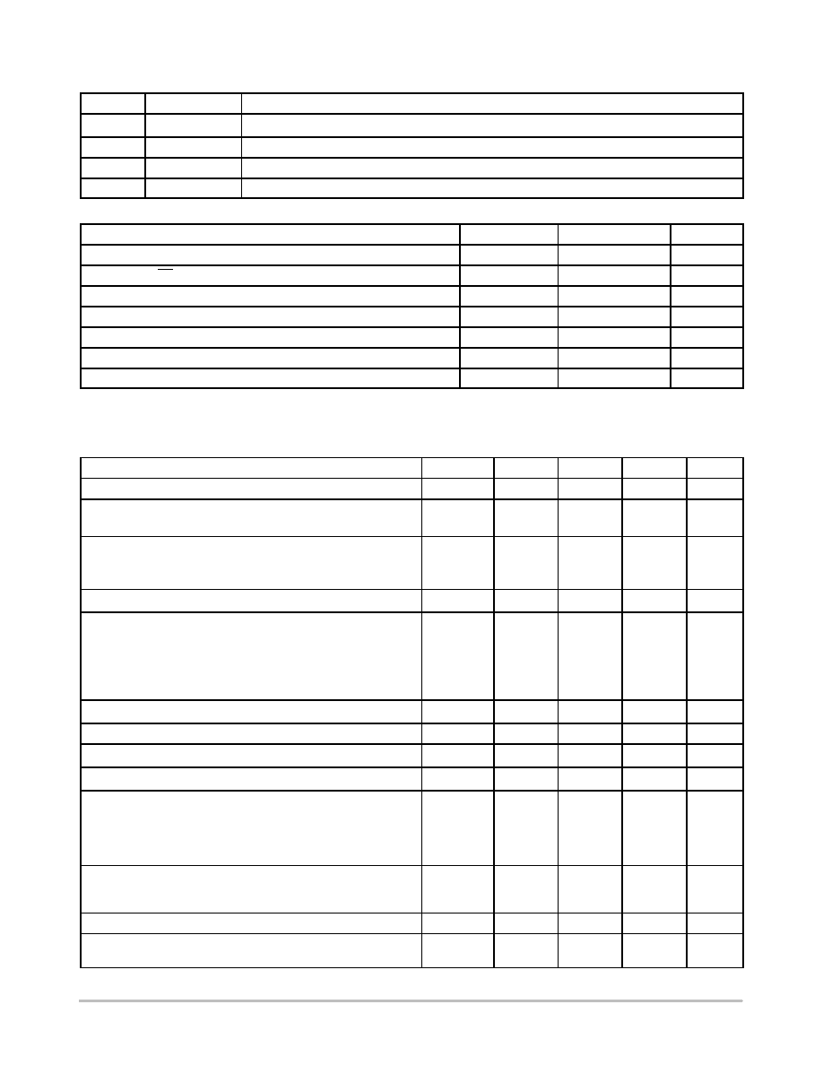
PIN FUNCTION DESCRIPTION
Pin
Symbol
Description
1
Vout
Regulated output voltage.
2
GND
Power supply ground.
3
CE
Chip enable pin.
4
V
in
Power supply input voltage.
MAXIMUM RATINGS
Rating
Symbol
Value
Unit
Input Voltage
V
in
6.5
V
Input Voltage (CE or CE Pin)
V
CE
-0.3 to V
in
+0.3
V
Output Voltage
V
out
-0.3 to V
in
+0.3
V
Output Current
I
out
140
mA
Power Dissipation
P
D
150
mW
Operating Junction Temperature Range
T
J
-40 to +85
∞
C
Storage Temperature Range
T
stg
-55 to +150
∞
C
Maximum ratings are those values beyond which device damage can occur. Maximum ratings applied to the device are individual stress limit values
(not normal operating conditions) and are not valid simultaneously. If these limits are exceeded, device functional operation is not implied, damage
may occur and reliability may be affected.
ELECTRICAL CHARACTERISTICS
(V
in
= V
out
+ 1.0 V, T
A
= 25
∞
C, unless otherwise noted.)
Characteristic
Symbol
Min
Typ
Max
Unit
Input Voltage
V
in
2.2
-
6.0
V
Output Voltage (I
out
= 1.0 mA to 30 mA)
V
out
V
out
X
0.985
-
V
out
X
1.015
V
Line Regulation (I
out
= 30 mA)
(V
out
+ 0.5 V
v
V
in
v
6.0 V)
(V
out
= 1.5 V, 2.2 V
v
V
in
v
6.0 V)
Reg
line
-
0.02
0.10
%/V
Load Regulation (I
out
= 1.0 mA to 120 mA)
Reg
load
-
12
40
mV
Dropout Voltage (I
out
= 120 mA)
V
out
= 1.5 V
V
out
= 1.8 V
V
out
= 2.5 V
2.8 V
v
V
out
v
3.3 V
V
DO
-
-
-
-
0.36
0.28
0.24
0.18
0.70
0.40
0.35
0.28
V
Quiescent Current (I
out
= 0 mA)
Iq
-
90
160
m
A
Output Current
I
out
120
-
-
mA
Shutdown Current (V
in
= V
CE
)
I
SD
0.1
1.0
m
A
Output Short Circuit Current (V
out
= 0)
I
lim
-
40
-
mA
Ripple Rejection (I
out
= 30 mA)
f = 1.0 kHz
(V
out
= 1.5 V, V
in
≠ V
out
= 1.2 V)
(V
out
w
2.5 V, V
in
≠ V
out
= 1.0 V)
RR
-
-
75
70
-
-
dB
Enable Input Threshold Voltage
High
Low
Vth
enh
Vth
enl
1.5
0
-
-
V
in
0.3
V
Output Noise Voltage (Bandwidth = 10 Hz to 100 kHz)
V
n
-
30
-
m
Vrms
Output Voltage Temperature Coefficient
(I
out
= 30 mA, -40
∞
C
v
T
A
v
85
∞
C)
D
V
out
/
D
T
-
"
100
-
ppm/
∞
C

NCP580
http://onsemi.com
3
TYPICAL CHARACTERISTICS
Figure 2. Output Voltage vs. Output Current
Figure 3. Output Voltage vs. Output Current
Figure 4. Output Voltage vs. Input Voltage
Figure 5. Output Voltage vs. Input Voltage
2.9
1.0
3.0
4.0
5.0
INPUT VOLTAGE V
in
(V)
OUTPUT VOL
T
AGE V
out
(V)
I
out
= 1.0 mA
6.0
I
out
= 30 mA
I
out
= 50 mA
3.0
0
100
200
250
OUTPUT CURRENT I
out
(mA)
OUTPUT VOL
T
AGE V
out
(V)
V
in
= 4.8 V
3.1 V
300
1.6
1.4
1.2
1.0
0.8
0.6
0.4
0.2
0
0
100
150
250
OUTPUT CURRENT I
out
(mA)
OUTPUT VOL
T
AGE V
out
(V)
V
in
= 3.5 V
2.5 V
1.8 V
2.0 V
300
2.5
2.0
1.5
1.0
0.5
0
3.8 V
3.3 V
1.0
2.0
3.0
4.0
INPUT VOLTAGE V
in
(V)
OUTPUT VOL
T
AGE V
out
(V)
I
out
= 1.0 mA
5.0
1.6
1.5
1.4
1.3
1.2
1.1
1.0
I
out
= 30 mA
I
out
= 50 mA
6.0
2.8
2.7
2.6
2.5
2.4
2.3
2.2
2.1
2.0
V
out
= 1.5 V
V
out
= 2.8 V
V
out
= 1.5 V
V
out
= 2.8 V
200
50
50
150
2.0
Figure 6. Quiescent Current vs. Input Voltage
100
1.0
2.0
3.0
4.0
INPUT VOLTAGE V
in
(V)
QUIESCENT CURRENT
, I
q
(
m
A)
5.0
6.0
80
70
60
50
40
30
20
10
0
0
V
out
= 1.5 V
90
Figure 7. Quiescent Current vs. Input Voltage
100
1.0
2.0
3.0
4.0
INPUT VOLTAGE V
in
(V)
5.0
6.0
80
70
60
50
40
30
20
10
0
0
V
out
= 2.8 V
90
QUIESCENT CURRENT
, I
q
(
m
A)

NCP580
http://onsemi.com
4
TYPICAL CHARACTERISTICS
Figure 8. Output Voltage vs. Temperature
Figure 9. Output Voltage vs. Temperature
-25
0
25
50
TEMPERATURE (
∞
C)
OUTPUT VOL
T
AGE, V
out
(V)
100
1.54
1.52
1.51
1.50
1.49
1.48
1.47
1.46
-50
V
in
= 2.5 V
I
out
= 30 mA
-25
0
25
50
TEMPERATURE (
∞
C)
OUTPUT VOL
T
AGE, V
out
(V)
100
2.86
2.84
2.82
2.80
2.78
2.76
2.74
-50
1.53
75
75
V
in
= 3.8 V
I
out
= 30 mA
V
out
= 1.5 V
V
out
= 2.8 V
Figure 10. Quiescent Current vs. Temperature
Figure 11. Quiescent Current vs. Temperature
0
50
100
TEMPERATURE (
∞
C)
120
110
100
90
80
70
60
-50
V
out
= 1.5 V
V
in
= 2.5 V
0
50
100
TEMPERATURE (
∞
C)
120
110
100
90
80
70
60
-50
V
out
= 2.8 V
V
in
= 3.8 V
QUIESCENT CURRENT
, I
q
(
m
A)
QUIESCENT CURRENT
, I
q
(
m
A)
Figure 12. Dropout Voltage vs. Output Current
20
40
60
80
OUTPUT CURRENT I
out
(mA)
DROPOUT VOL
T
AGE, V
DO
(V)
120
1.2
1.0
0.8
0.6
0.4
0.2
0.0
0
V
out
= 1.5 V
100
-40
∞
C
85
∞
C
25
∞
C
Figure 13. Dropout Voltage vs. Output Current
20
40
60
80
OUTPUT CURRENT I
out
(mA)
DROPOUT VOL
T
AGE, V
DO
(V)
120
0.25
0.20
0.15
0.10
0.05
0.00
0
V
out
= 2.8 V
100
-40
∞
C
85
∞
C
25
∞
C

NCP580
http://onsemi.com
5
TYPICAL CHARACTERISTICS
Figure 14. Ripple Rejection vs. Frequency
Figure 15. Ripple Rejection vs. Frequency
90
1
10
FREQUENCY, f (kHz)
RIPPLE REJECTION, RR (dB)
100
80
70
60
50
40
30
20
10
0
0.1
V
out
= 1.5 V
V
in
= 2.5 Vdc + 0.5 Vp-p
C
out
= Ceramic 2.2
m
F
90
1
10
FREQUENCY, f (kHz)
RIPPLE REJECTION, RR (dB)
100
80
70
60
50
40
30
20
10
0
0.1
V
out
= 2.8 V
V
in
= 3.8 Vdc + 0.5 Vp-p
C
out
= Ceramic 2.2
m
F
I
out
= 1.0 mA
I
out
= 30 mA
I
out
= 50 mA
I
out
= 1.0 mA
I
out
= 30 mA
I
out
= 50 mA